

Page 1

3D7503
Doc #98009 DATA DELAY DEVICES, INC. 1
12/11/98 3 Mt. Prospect Ave. Clifton, NJ 07013
MONOLITHIC MANCHESTER
ENCODER/DECODER
(SERIES 3D7503)
FEATURES
• All-silicon, low-power CMOS technology
• Encoder and decoder function independently
• Encoder has buffered clock output
• TTL/CMOS compatible inputs and outputs
• Vapor phase, IR and wave solderable
• Auto-insertable (DIP pkg.)
• Low ground bounce noise
• Maximum data rate: 50 MBaud
• Data rate range: ±15%
• Lock-in time: 1 bit
FUNCTIONAL DESCRIPTION
The 3D7503 is a monolithic CMOS Manchester Encoder/Decoder combo
chip. The device uses bi-phase-level encoding to embed a clock signal
into a data stream for transmission across a communications link. In this
encoding mode, a logic one is represented by a high-to-low transition in
the center of the bit cell, while a logic zero is represented by a low-to-high
transition.
The Manchester encoder combines the clock (CIN) and data (DIN) into a
single bi-phase-level signal (TX). An inverted version of this signal (TXB)
is also available. The data baud rate (in MBaud) is equal to the input
clock frequency (in MHz). A replica of the clock input is also available
(CBUF).
The encoder may be reset by setting the RESB input low; otherwise, it
should be left high. The TX and TXB signals may be disabled (high-Z) by
setting TXENB high. Similarly, CBUF may be disabled by setting CEN
low. Under most operating conditions, the encoder is never reset, TX and
TXB are always enabled, and CBUF is not used. With this in mind, the
3D7503 provides an internal pull-up resistor on RESB and internal pulldown resistors on CEN and TXENB, so that most users can leave these inputs uncommitted.
The Manchester decoder accepts the embedded-clock signal at the RX input. The recovered clock and
data signals are presented on COUT and DOUTB, respectively, with the data signal inverted. The
operating baud rate (in MBaud) is specified by the dash number of the device. The input baud rate may
vary by as much as ±15% from the nominal device baud rate without compromising the integrity of the
information received.
Because the decoder is not PLL-based, it does not require a long preamble in order to lock onto the
received signal. Rather, the device requires at most one bit cell before the data presented at the output is
valid. This is extremely useful in cases where the information arrives in bursts and the input is otherwise
turned off.
Normally, the encoder and decoder function independently. However, if the LOOP input is set high, the
encoded TX signal is fed back internally into the decoder and the RX input is ignored. This feature is
useful for diagnostics. The LOOP input has an internal pull-down resistor and may be left uncommitted if
this feature is not needed.
data
delay
devices, inc.
3
PACKAGES
14
13
12
11
10
9
8
1
2
3
4
5
6
7
CIN
CEN
RX
COUT
DIN
RESB
GND
VDD
CBUF
LOOP
TXENB
DOUTB
TXB
TX
3D7503-xxx DIP (.300)
3D7503G-xxx Gull Wing (.300)
3D7503D-xxx SOIC (.150)
PIN DESCRIPTIONS
Encoder:
CIN Clock Input
DIN Data Input
RESB Reset
CEN Clock buffer enable
TXENB Transmit enable
CBUF Buffered clock
TX,TXB Transmitted signal
Decoder:
RX Received Signal
COUT Recovered Clock
DOUTB Recovered Data
Common:
LOOP Loop enable
VDD +5 Volts
GND Ground
1998 Data Delay Devices
Page 2
3D7503
Doc #98009 DATA DELAY DEVICES, INC. 2
12/11/98 Tel: 973-773-2299 Fax: 973-773-9672 http://www.datadelay.com
TABLE 1: PART NUMBER SPECIFICATIONS
PART DECODER BAUD RATE (MBaud)
NUMBER Nominal Minimum Maximum
3D7503-5 5.00 4.25 5.75
3D7503-10 10.00 8.50 11.50
3D7503-20 20.00 17.00 23.00
3D7503-25 25.00 21.25 28.75
3D7503-30 30.00 25.50 34.50
3D7503-40 40.00 34.00 46.00
3D7503-50 50.00 42.50 57.50
NOTE: Any baud rate between 5 and 50 MBaud not shown is also available at no extra cost.
APPLICATION NOTES
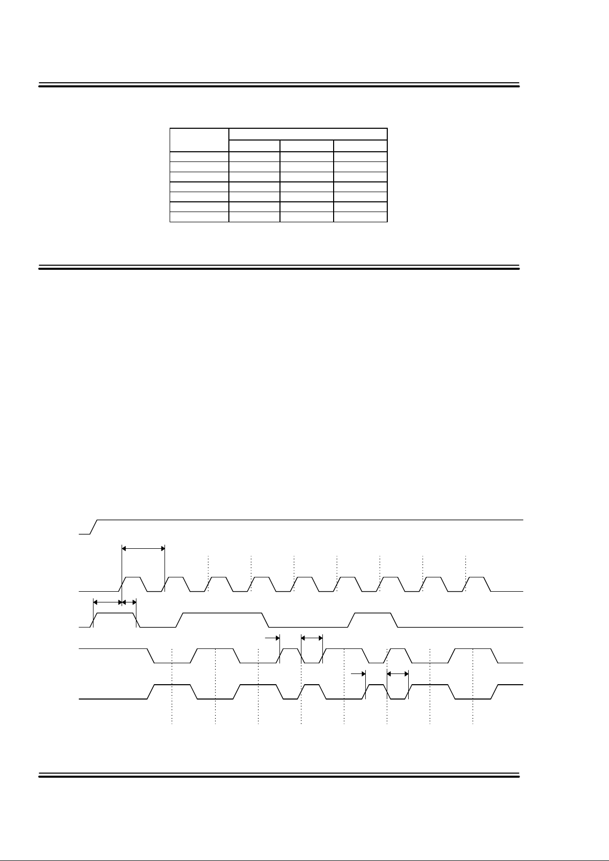
ENCODER
The Manchester encoder subsystem samples the
data input at the rising edge of the input clock.
The sampled data is used in conjunction with the
clock rising and falling edges to generate the byphase level Manchester code.
The encoder employs the timing of the clock
rising and falling edges (duty cycle) to implement
the required coding scheme, as shown in Figure
1. To reduce the difference between the output
data high time and low time, it is essential that
the deviation of the input clock duty cycle from
50/50 be minimized.
The encoder presents at its outputs the true and
the complimented encoded data. The High-toLow time skew of the selected data output should
be budgeted by the user, as it relates to his
application, to satisfactorily estimate the
distortion of the transmitted data stream. Such
an estimate is very useful in determining the
functionality and margins of the data link, if a
Manchester decoder is used to decode the
received data.
RESET
(RESB)
CLOCK
(CIN)
DATA
(DIN)
TRANSMIT
(TX)
TRANSMIT
(TXB)
t
DS
t
DH
Figure 1: Timing Diagram (Encoder)
1/f
C
1 0 1 1 0 0 1 0
1 0 1 1 0 0 1 0
(Left high for normal operation)
T
2H
T
2L
T
1H
T
1L
Page 3

3D7503
Doc #98009 DATA DELAY DEVICES, INC. 3
12/11/98 3 Mt. Prospect Ave. Clifton, NJ 07013
APPLICATION NOTES (CONT’D)
DECODER
The Manchester decoder subsystem samples the
input at precise pre-selected intervals to retrieve
the data and to recover the clock from the
received data stream. Its architecture comprises
finely tuned delay elements and proprietary
circuitry which, in conjunction with other circuits,
implement the data decoding and clock recovery
function.
Typically, the encoded data transmitted from a
source arrives at the decoder corrupted. Such
corruption of the received data manifests itself
as jitter and/or pulse width distortion at the
decoder input. The instantaneous deviations
from nominal Baud Rate and/or Pulse Width
(high or low) adversely impact the data
extraction and clock recovery function if their
published limits are exceeded. See Table 4,
Allowed Baud Rate/Duty Cycle. The decoder,
being a self-timed device, is tolerant of
frequency modulation (jitter) present in the input
data stream, provided that the input data pulse
width variations remain within the allowable
ranges.
The decoder presents at its outputs the decoded
data (inverted) and the recovered clock. The
decoded data is valid at the rising edge of the
clock.
The clock recovery function operates in two
modes dictated by the input data stream bit
sequence. When a data bit is succeeded by its
inverse, the clock recovery circuit is engaged
and forces the clock output low for a time equal
to one over twice the baud rate. Otherwise,
the input is presented at the clock output
unchanged, shifted in time. Therefore, the clock
duty cycle is strongly dependent on the baud
rate, as this will affect the clock-high duration.
The clock output falling edge is not operated on
by the clock recovery circuitry. It, therefore,
preserves more accurately the clock frequency
information embedded in the transmitted data. It
can therefore be used, if desired, to retrieve
clock frequency information.
INPUT SIGNAL CHARACTERISTICS
The 3D7503 inputs are TTL compatible. The
user should assure him/herself that the 1.5
volt TTL threshold is used when referring to all
timing, especially to the input clock duty cycle
(encoder) and the received data (decoder).
POWER SUPPLY AND
TEMPERATURE CONSIDERATIONS
CMOS integrated circuitry is strongly dependent
on power supply and temperature. The
monolithic 3D7503 Manchester encoder/decoder
utilizes novel and innovative compensation
circuitry to minimize timing variations induced by
fluctuations in power supply and/or temperature.
Nevertheless, optimum performance is achieved
by providing a stable power supply and a clean
ground plane, and by placing a bypass capacitor
(0.1uf typically) as close to the device as
possible.
CLOCK
(CLK)
RECEIVED
(RX)
Figure 2: Timing Diagram (Decoder)
t
C
DECODED
1 0 1 1 0 0 1
ENCODED
1 0 1 1 0 0 10
DATA
(DATB)
t
CL
t
CWL
t
CD
Page 4

3D7503
Doc #98009 DATA DELAY DEVICES, INC. 4
12/11/98 Tel: 973-773-2299 Fax: 973-773-9672 http://www.datadelay.com
DEVICE SPECIFICATIONS
TABLE 2: ABSOLUTE MAXIMUM RATINGS
PARAMETER SYMBOL MIN MAX UNITS NOTES
DC Supply Voltage V
DD
-0.3 7.0 V
Input Pin Voltage V
IN
-0.3 VDD+0.3 V
Input Pin Current I
IN
-10 10 mA 25C
Storage Temperature T
STRG
-55 150 C
Lead Temperature T
LEAD
300 C 10 sec
TABLE 3: DC ELECTRICAL CHARACTERISTICS
(0C to 70C, 4.75V to 5.25V)
PARAMETER SYMBOL MIN MAX UNITS NOTES
Static Supply Current* I
DD
40 mA
High Level Input Voltage V
IH
2.0 V
Low Level Input Voltage V
IL
0.8 V
High Level Input Current I
IH
1.0
µA
VIH = V
DD
Low Level Input Current I
IL
1.0
µA
VIL = 0V
High Level Output Current I
OH
-4.0 mA VDD = 4.75V
VOH = 2.4V
Low Level Output Current I
OL
4.0 mA VDD = 4.75V
VOL = 0.4V
Output Rise & Fall Time TR & T
F
2 ns CLD = 5 pf
*IDD(Dynamic) = 2 * CLD * VDD * F Input Capacitance = 10 pf typical
where: CLD = Average capacitance load/pin (pf) Output Load Capacitance (CLD) = 25 pf max
F = Input frequency (GHz)
TABLE 4: AC ELECTRICAL CHARACTERISTICS
(0C to 70C, 4.75V to 5.25V, except as noted)
PARAMETER
SYMBOL
MIN TYP MAX UNITS NOTES
Input Baud Rate (Encoder)
f
BN
50 MBaud
Clock Frequency
f
C
50 MHz
Data set-up to clock rising
t
DS
3.5 ns
Data hold from clock rising
t
DH
0 ns
TX High-Low time skew
t1H - t
1L
-3.5 3.5 ns 1
TXB High-Low time skew
t2H - t
2L
-2.0 2.0 ns 1
TX - TXB High/Low time skew
t1H - t
2L
-3.0 3.0 ns 1
Nominal Input Baud Rate (Decoder)
f
BN
5 50 MBaud
Allowed Input Baud Rate Deviation
f
B
-0.15 f
BN
0.15 f
BN
MBaud 25C, 5.00V
Allowed Input Baud Rate Deviation
f
B
-0.05 f
BN
0.05 f
BN
MBaud -40C to 85C
4.75V to 5.25V
Allowed Input Baud Rate Deviation
f
B
-0.03 f
BN
0.03 f
BN
MBaud -55C to 125C
4.75V to 5.25V
Allowed Input Duty Cycle
42.5 50.0 57.5 %
Bit Cell Time
tc 1000/f
B
ns
Input Data Edge to Clock Falling Edge
t
CL
0.75 tc ns
Clock Width Low
t
CWL
500/f
BN
ns
±2ns or 5%
Clock Falling Edge to Data Transition
t
CD
3.0 4.0 5.0 ns
Notes: 1: Assumes a 50% duty cycle clock input
Page 5

3D7503
Doc #98009 DATA DELAY DEVICES, INC. 5
12/11/98 3 Mt. Prospect Ave. Clifton, NJ 07013
AUTOMATED TESTING - MONOLITHIC PRODUCTS
TEST CONDITIONS
INPUT: OUTPUT:
Ambient Temperature: 25oC ± 3oC R
load
: 10KΩ ± 10%
Supply Voltage (Vcc): 5.0V ± 0.1V C
load
: 5pf ± 10%
Input Pulse: High = 3.0V ± 0.1V Threshold: 1.5V (Rising & Falling)
Low = 0.0V ± 0.1V
Source Impedance: 50Ω Max.
Rise/Fall Time: 3.0 ns Max. (measured
between 0.6V and 2.4V )
Pulse Width: PWIN = 1/(2*BAUD)
Period: PERIN = 1/BAUD
NOTE: The above conditions are for test only and do not in any way restrict the operation of the device.
10KΩ
470Ω
5pf
Device
Under
Test
Digital
Scope
OUT
TRIGINTRIG
Figure 3: Test Setup
DEVICE UNDER
TEST (DUT)
DIGITAL SCOPE
WAVEFORM
GENERATOR
OUT
IN
COMPUTER
SYSTEM
PRINTER
Figure 4: Timing Diagram
t
PLH
t
PHL
PER
IN
PW
IN
t
RISE
t
FALL
0.6V
0.6V
1.5V
1.5V
2.4V
2.4V
1.5V
1.5V
V
IH
V
IL
V
OH
V
OL
INPUT
SIGNAL
OUTPUT
SIGNAL
 Loading...