

Page 1
3D7502
Doc #97032 DATA DELAY DEVICES, INC. 1
5/19/97 3 Mt. Prospect Ave. Clifton, NJ 07013
MONOLITHIC MANCHESTER
DECODER
(SERIES 3D7502)
FEATURES
• All-silicon, low-power CMOS
technology
• TTL/CMOS compatible inputs and
outputs
• Vapor phase, IR and wave
solderable
• Auto-insertable (DIP pkg.)
• Low ground bounce noise
• Maximum data rate: 50 MBaud
• Data rate range: ±15%
FUNCTIONAL DESCRIPTION
The 3D7502 product family consists of monolithic CMOS Manchester
Decoders. The unit accepts at the RX input a bi-phase-level,
embedded-clock signal. In this encoding mode, a logic one is
represented by a high-to-low transition within the bit cell, while a logic
zero is represented by a low-to-high transition. The recovered clock
and data signals are presented on CLK and DATB, respectively, with
the data signal inverted. The operating baud rate (in MBaud) is specified by the dash number. The input
baud rate may vary by as much as ±15% from the nominal device baud rate without compromising the
integrity of the information received.
Because the 3D7502 is not PLL-based, it does not require a long preamble in order to lock onto the
received signal. Rather, the device requires at most one bit cell before the data presented at the output is
valid. This is extremely useful in cases where the information arrives in bursts and the input is otherwise
turned off.
The all-CMOS 3D7502 integrated circuit has been designed as a reliable, economic alternative to hybrid
TTL Manchester Decoders. It is TTL- and CMOS-compatible, capable of driving ten 74LS-type loads. It is
offered in standard 8-pin and 14-pin auto-insertable DIPs and space saving surface mount 8-pin and 14pin SOICs.
TABLE 1: PART NUMBER SPECIFICATIONS
PART BAUD RATE (MBaud)
NUMBER Nominal Minimum Maximum
3D7502-5 5.00 4.25 5.75
3D7502-10 10.00 8.50 11.50
3D7502-20 20.00 17.00 23.00
3D7502-25 25.00 21.25 28.75
3D7502-30 30.00 25.50 34.50
3D7502-40 40.00 34.00 46.00
3D7502-50 50.00 42.50 57.50
NOTES: Any baud rate between 5 and 50 MBaud not shown is also available at no extra cost. 1997 Data Delay Devices
data
delay
devices, inc.
3
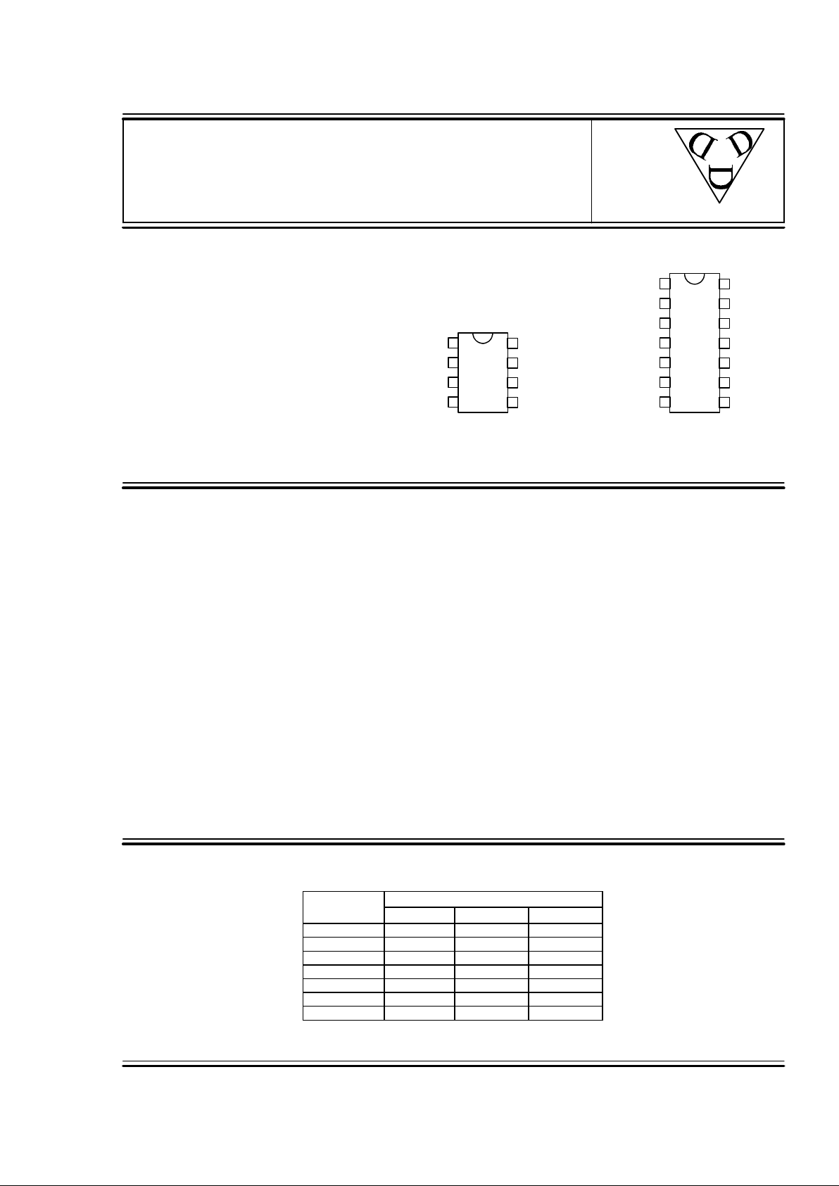
PACKAGES
8
7
6
5
1
2
3
4
RX
CLK
N/C
GND
VDD
N/C
N/C
DATB
3D7502M-xxx DIP (.300)
3D7502H-xxx Gull Wing (.300)
3D7502Z-xxx SOIC (.150)
14
13
12
11
10
9
8
1
2
3
4
5
6
7
RX
N/C
N/C
CLK
N/C
N/C
GND
VDD
N/C
N/C
N/C
N/C
N/C
DATB
3D7502-xxx DIP (.300)
3D7502G-xxx Gull Wing (.300)
3D7502D-xxx SOIC (.150)
PIN DESCRIPTIONS
RX Signal Input
CLK Signal Output (Clock)
DATB Signal Output (Data)
VCC +5 Volts
GND Ground
Page 2

3D7502
Doc #97032 DATA DELAY DEVICES, INC. 2
5/19/97 Tel: 973-773-2299 Fax: 973-773-9672 http://www.datadelay.com
APPLICATION NOTES
The 3D7502 Manchester Decoder samples the
input at precise pre-selected intervals to retrieve
the data and to recover the clock from the
received data stream. Its architecture comprises
finely tuned delay elements and proprietary
circuitry which, in conjunction with other circuits,
implement the data decoding and clock recovery
function.
INPUT SIGNAL CHARACTERISTICS
Encoded data transmitted from a source arrives
at its destination corrupted. Such corruption of
the received data manifests itself as jitter and/or
pulse width distortion at the input to the device.
The instantaneous deviations from nominal Baud
Rate and/or Pulse Width (high or low) adversely
impact the data extraction and clock recovery
function if their published limits are exceeded.
See Table 4, Allowed Baud Rate/Duty Cycle.
The 3D7502 Manchester Decoder Data Input is
TTL compatible. The user should assure
himself that the 1.5 volt TTL threshold is used
when referring to all timing, especially the input
pulse widths.
FREQUENCY (JITTER) ERRORS
The 3D7502 Manchester Decoder, being a selftimed device, is tolerant of frequency
modulation (jitter) present in the input data
stream, provided that the input data pulse width
variations remain within the allowable ranges.
OUTPUT SIGNAL CHARACTERISTICS
The 3D7502 presents at its outputs the decoded
data (inverted) and the recovered clock. The
decoded data is valid at the rising edge of the
clock.
The clock recovery function operates in two
modes dictated by the input data stream bit
sequence. When a data bit is succeeded by its
inverse, the clock recovery circuit is engaged
and forces the clock output low for a time equal
to one over twice the baud rate. Otherwise,
the input is presented at the clock output
unchanged, shifted in time.
When engaged, the clock recovery circuit
generates a low-going pulse of fixed width.
Therefore, the clock duty cycle is strongly
dependent on the baud rate, as this will affect
the clock-high duration.
The clock output falling edge is not operated on
by the clock recovery circuitry. It, therefore,
preserves more accurately the clock frequency
information embedded in the transmitted data.
Therefore, it can be used, if it is desired, to
retrieve clock frequency information.
POWER SUPPLY AND
TEMPERATURE CONSIDERATIONS
CMOS integrated circuitry is strongly dependent
on power supply and temperature. The
monolithic 3D7502 Manchester Decoder utilizes
novel and innovative compensation circuitry to
minimize timing variations induced by
fluctuations in power supply and/or temperature.
CLOCK
(CLK)
RECEIVED
(RX)
Figure 1: Timing Diagram
t
C
DECODED
1 0 1 1 0 0 1
ENCODED
1 0 1 1 0 0 10
DATA
(DATB)
t
CL
t
CWL
t
CD
Page 3

3D7502
Doc #97032 DATA DELAY DEVICES, INC. 3
5/19/97 3 Mt. Prospect Ave. Clifton, NJ 07013
.
DEVICE SPECIFICATIONS
TABLE 2: ABSOLUTE MAXIMUM RATINGS
PARAMETER SYMBOL MIN MAX UNITS NOTES
DC Supply Voltage V
DD
-0.3 7.0 V
Input Pin Voltage V
IN
-0.3 VDD+0.3 V
Input Pin Current I
IN
-10 10 mA 25C
Storage Temperature T
STRG
-55 150 C
Lead Temperature T
LEAD
300 C 10 sec
TABLE 3: DC ELECTRICAL CHARACTERISTICS
(0C to 70C, 4.75V to 5.25V)
PARAMETER SYMBOL MIN MAX UNITS NOTES
Static Supply Current* I
DD
40 mA
High Level Input Voltage V
IH
2.0 V
Low Level Input Voltage V
IL
0.8 V
High Level Input Current I
IH
1.0
µA
VIH = V
DD
Low Level Input Current I
IL
1.0
µA
VIL = 0V
High Level Output Current I
OH
-4.0 mA VDD = 4.75V
VOH = 2.4V
Low Level Output Current I
OL
4.0 mA VDD = 4.75V
VOL = 0.4V
Output Rise & Fall Time TR & T
F
2 ns CLD = 5 pf
*IDD(Dynamic) = 2 * CLD * VDD * F Input Capacitance = 10 pf typical
where: CLD = Average capacitance load/pin (pf) Output Load Capacitance (CLD) = 25 pf max
F = Input frequency (GHz)
TABLE 4: AC ELECTRICAL CHARACTERISTICS
(0C to 70C, 4.75V to 5.25V, except as noted)
PARAMETER
SYMBOL
MIN TYP MAX UNITS NOTES
Nominal Input Baud Rate f
BN
5 50 MBaud
Allowed Input Baud Rate Deviation f
B
-0.15 f
BN
0.15 f
BN
MBaud 25C, 5.00V
Allowed Input Baud Rate Deviation f
B
-0.05 f
BN
0.05 f
BN
MBaud -40C to 85C
4.75V to 5.25V
Allowed Input Baud Rate Deviation f
B
-0.03 f
BN
0.03 f
BN
MBaud -55C to 125C
4.75V to 5.25V
Allowed Input Duty Cycle 42.5 50.0 57.5 %
Bit Cell Time tc 1000/f
B
ns
Input Data Edge to Clock Falling Edge t
CL
0.75 tc ns
Clock Width Low t
CWL
500/f
BN
ns
±2ns or 5%
Clock Falling Edge to Data Transition t
CD
3.0 4.0 5.0 ns
Page 4

3D7502
Doc #97032 DATA DELAY DEVICES, INC. 4
5/19/97 Tel: 973-773-2299 Fax: 973-773-9672 http://www.datadelay.com
SILICON DELAY LINE AUTOMATED TESTING
TEST CONDITIONS
INPUT: OUTPUT:
Ambient Temperature: 25oC ± 3oC R
load
: 10KΩ ± 10%
Supply Voltage (Vcc): 5.0V ± 0.1V C
load
: 5pf ± 10%
Input Pulse: High = 3.0V ± 0.1V Threshold: 1.5V (Rising & Falling)
Low = 0.0V ± 0.1V
Source Impedance: 50Ω Max.
Rise/Fall Time: 3.0 ns Max. (measured
between 0.6V and 2.4V )
Pulse Width: PWIN = 1/(2*BAUD)
Period: PERIN = 1/BAUD
NOTE: The above conditions are for test only and do not in any way restrict the operation of the device.
10KΩ
470Ω
5pf
Device
Under
Test
Digital
Scope
OUT
TRIGINTRIG
Figure 2: Test Setup
DEVICE UNDER
TEST (DUT)
DIGITAL SCOPE
WAVEFORM
GENERATOR
OUT
IN
COMPUTER
SYSTEM
PRINTER
Figure 3: Timing Diagram
t
PLH
t
PHL
PER
IN
PW
IN
t
RISE
t
FALL
0.6V
0.6V
1.5V
1.5V
2.4V
2.4V
1.5V
1.5V
V
IH
V
IL
V
OH
V
OL
INPUT
SIGNAL
OUTPUT
SIGNAL
 Loading...