

Page 1
3D7408
Doc #96003 DATA DELAY DEVICES, INC. 1
12/2/96 3 Mt. Prospect Ave. Clifton, NJ 07013
MONOLITHIC 8-BIT
PROGRAMMABLE DELAY LINE
(SERIES 3D7408)
FEATURES
• All-silicon, low-power CMOS technology
• TTL/CMOS compatible inputs and outputs
• Vapor phase, IR and wave solderable
• Auto-insertable (DIP pkg.)
• Low ground bounce noise
• Leading- and trailing-edge accuracy
• Increment range: 0.25 through 5.0ns
• Delay tolerance: 1% (See Table 1)
• Temperature stability: ±3% typical (0C-70C)
• Vdd stability: ±1% typical (4.75V-5.25V)
• Minimum input pulse width: 10% of total
delay
• Programmable via 3-wire serial or 8-bit
parallel interface
FUNCTIONAL DESCRIPTION
The 3D7408 Programmable 8-Bit Silicon Delay Line product
family consists of 8-bit, user-programmable CMOS silicon
integrated circuits. Delay values, programmed either via the
serial or parallel interface, can be varied over 255 equal steps
ranging from 250ps to 5.0ns inclusively. Units have a typical
inherent (zero step) delay of 12ns to 17ns (See Table 1). The
input is reproduced at the output without inversion, shifted in time
as per user selection. The 3D7408 is TTL- and CMOScompatible, capable of driving ten 74LS-type loads, and features
both rising- and falling-edge accuracy.
The all-CMOS 3D7408 integrated circuit has been designed as a reliable, economic alternative to hybrid
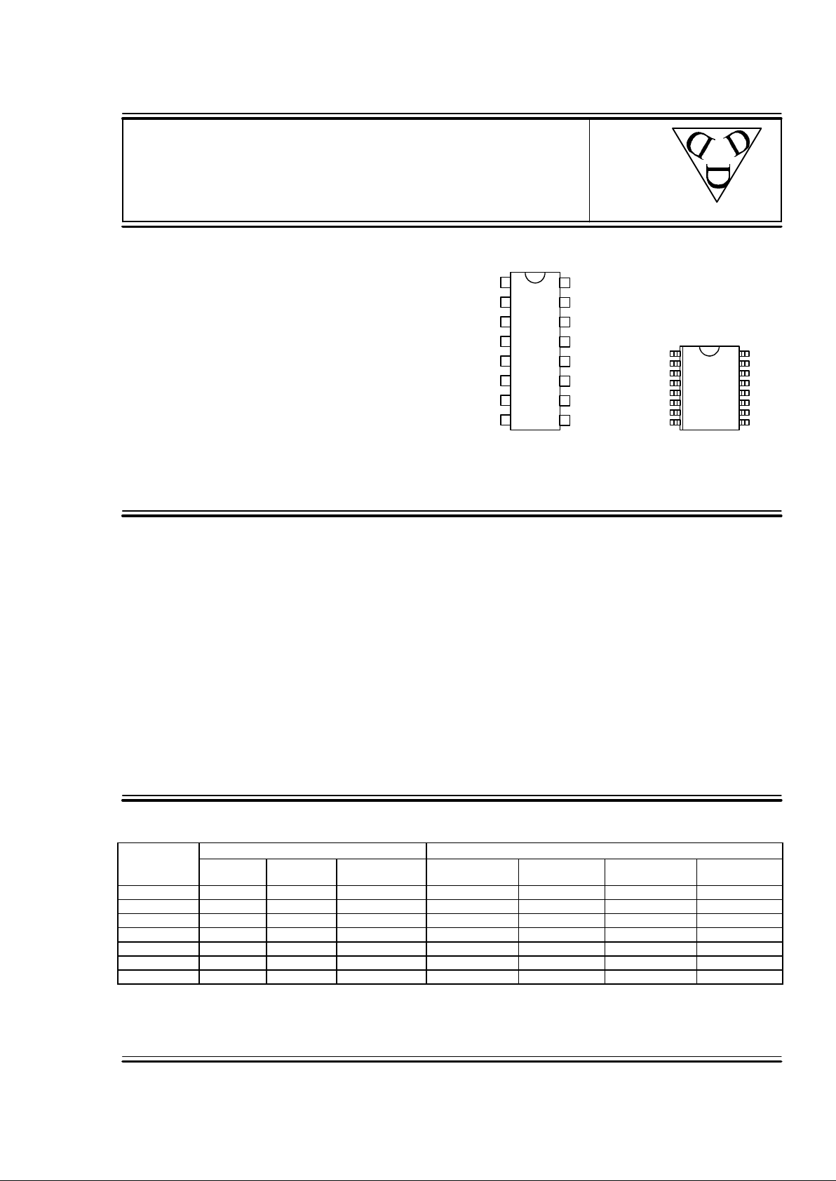
TTL programmable delay lines. It is offered in a standard 16-pin auto-insertable DIP and a space saving
surface mount 16-pin SOIC.
PACKAGES
16
15
14
13
12
11
10
9
1
2
3
4
5
6
7
8
IN
AE
SO/P0
P1
P2
P3
P4
GND
VDD
OUT
MD
P7
P6
SC
P5
SI
3D7408 DIP
3D7408G Gull Wing
(300 Mil)
1
2
3
4
5
6
7
8
16
15
14
13
12
11
10
9
IN
AE
SO/P0
P1
P2
P3
P4
GND
VDD
OUT
MD
P7
P6
SC
P5
SI
3D7408S
SOIC
(300 Mil)
data
delay
devices, inc.
3
(For mechanical data, see Case Dimensions document)
PIN DESCRIPTIONS
IN Signal Input
OUT Signal Output
MD Mode Select
AE Address Enable
P0-P7 Parallel Data Input
SC Serial Clock
SI Serial Data Input
SO Serial Data Output
VCC +5 Volts
GND Ground
TABLE 1: PART NUMBER SPECIFICATIONS
PART DELAYS AND TOLERANCES INPUT RESTRICTIONS
NUMBER
Step 0
Delay (ns)
Step 255
Delay (ns)
Delay
Increment (ns)
Max Operating
Frequency
Absolute Max
Oper Freq
Min Operating
P.W.
Absolute Min
Oper P.W.
3D7408-0.25
12 ± 2 75.75 ± 4.0 0.25 ± 0.15
6.25 MHz 90 MHz 80.0 ns 5.5 ns
3D7408-0.5
12 ± 2 139.5 ± 4.0 0.50 ± 0.25
3.15 MHz 45 MHz 160.0 ns 11.0 ns
3D7408-1
12 ± 2 267.0 ± 5.0 1.00 ± 0.50
1.56 MHz 22 MHz 320.0 ns 22.0 ns
3D7408-2
14 ± 2 522.0 ± 6.0 2.00 ± 1.00
0.78 MHz 11 MHz 640.0 ns 44.0 ns
3D7408-3
17 ± 2 782.0 ± 8.0 3.00 ± 1.50
0.52 MHz 7.5 MHz 960.0 ns 66.0 ns
3D7408-4
17 ± 2 1037 ± 9.0 4.00 ± 2.00
0.39 MHz 5.5 MHz 1280.0 ns 88.0 ns
3D7408-5
17 ± 2 1292 ± 10 5.00 ± 2.50
0.31 MHz 4.4 MHz 1600.0 ns 110.0 ns
NOTES: Any delay increment between 0.25 and 5.0 ns not shown is also available.
All delays referenced to input pin 1996 Data Delay Devices
Page 2

3D7408
Doc #96003 DATA DELAY DEVICES, INC. 2
12/2/96 Tel: 973-773-2299 Fax: 973-773-9672 http://www.datadelay.com
APPLICATION NOTES
The 8-bit programmable 3D7408 delay line
architecture is comprised of a number of delay
cells connected in series with their respective
outputs multiplexed onto the Delay Out pin
(OUT) by the user-selected programming data.
Each delay cell produces at its output a replica of
the signal present at its input, shifted in time.
INPUT SIGNAL CHARACTERISTICS
The Frequency and/or Pulse Width (high or low)
of operation may adversely impact the specified
delay and increment accuracy of the particular
device. The reasons for the dependency of the
output delay accuracy on the input signal
characteristics are varied and complex.
Therefore a Maximum and an Absolute
Maximum operating input frequency and a
Minimum and an Absolute Minimum operating
pulse width have been specified.
OPERATING FREQUENCY
The Absolute Maximum Operating Frequency
specification, tabulated in Table 1, determines
the highest frequency of the delay line input
signal that can be reproduced, shifted in time at
the device output, with acceptable duty cycle
distortion.
The Maximum Operating Frequency
specification determines the highest frequency of
the delay line input signal for which the output
delay accuracy is guaranteed.
To guarantee the Table 1 delay accuracy for
input frequencies higher than the Maximum
Operating Frequency, the 3D7408 must be
tested at the user operating frequency.
Therefore, to facilitate production and device
identification, the part number will include a
custom reference designator identifying the
intended frequency of operation. The
programmed delay accuracy of the device is
guaranteed, therefore, only at the user specified
input frequency. Small input frequency variation
about the selected frequency will only marginally
impact the programmed delay accuracy, if at all.
Nevertheless, it is strongly recommended
that the engineering staff at DATA DELAY
DEVICES be consulted.
OPERATING PULSE WIDTH
The Absolute Minimum Operating Pulse
Width (high or low) specification, tabulated in
Table 1, determines the smallest Pulse Width of
the delay line input signal that can be
reproduced, shifted in time at the device output,
with acceptable pulse width distortion.
The Minimum Operating Pulse Width (high or
low) specification determines the smallest Pulse
Width of the delay line input signal for which the
output delay accuracy tabulated in Table 1 is
guaranteed.
To guarantee the Table 1 delay accuracy for
input pulse width smaller than the Minimum
Operating Pulse Width, the 3D7408 must be
tested at the user operating pulse width.
Therefore, to facilitate production and device
identification, the part number will include a
custom reference designator identifying the
intended frequency and duty cycle of operation.
The programmed delay accuracy of the device is
guaranteed, therefore, only for the user specified
input characteristics. Small input pulse width
variation about the selected pulse width will only
marginally impact the programmed delay
accuracy, if at all. Nevertheless, it is strongly
recommended that the engineering staff at
DATA DELAY DEVICES be consulted.
SPECIAL HIGH ACCURACY
REQUIREMENTS
The Table 1 delay and increment accuracy
specifications are aimed at meeting the
requirements of the majority of the applications
encountered to date. However, some systems
may place tighter restrictions on one accuracy
parameter in favor of others. For example, a
channel delay equalizing system is concerned in
minimizing delay variations among the various
channels. Therefore, because the inter channel
skew is a delay difference, the programmed
delay tolerance may need to be considerably
decreased, while the increment and its tolerance
are of no consequence. The opposite is true for
an under-sampled multi-channel data acquisition
system.
Page 3

3D7408
Doc #96003 DATA DELAY DEVICES, INC. 3
12/2/96 3 Mt. Prospect Ave. Clifton, NJ 07013
APPLICATION NOTES (CONT’D)
The flexible 3D7408 architecture can be
exploited to conform to these more demanding
user-dictated accuracy constraints. However, to
facilitate production and device identification, the
part number will include a custom reference
designator identifying the user requested
accuracy specifications and operating conditions.
It is strongly recommended that the
engineering staff at DATA DELAY DEVICES
be consulted.
POWER SUPPLY AND
TEMPERATURE CONSIDERATIONS
The delay of CMOS integrated circuits is strongly
dependent on power supply and temperature.
The monolithic 3D7408 programmable delay line
utilizes novel and innovative compensation
circuitry to minimize the delay variations induced
by fluctuations in power supply and/or
temperature.
The thermal coefficient is reduced to 600
PPM/C, which is equivalent to a variation, over
the 0C-70 C operating range, of ±±3% from the
room-temperature delay settings. The power
supply coefficient is reduced, over the 4.75V-
5.25V operating range, to ±±1% of the delay
settings at the nominal 5.0VDC power supply
and/or ±±2ns, whichever is greater.
It is essential that the power supply pin be
adequately bypassed and filtered. In
addition, the power bus should be of as low
an impedance construction as possible.
Power planes are preferred.
PROGRAMMED DELAY (ADDRESS)
UPDATE
A delay line is a memory device. It stores
information present at the input for a time equal
to the delay setting before presenting it at the
output with minimal distortion. The 3D7408 8-bit
programmable delay line can be represented by
256 serially connected delay elements
(individually addressed by the programming
data), each capable of storing data for a time
equal to the device increment (step time). The
delay line memory property, in conjunction with
the operational requirement of “instantaneously”
connecting the delay element addressed by the
programming data to the output, may inject
spurious information onto the output data stream.
In order to ensure that spurious outputs do not
occur, it is essential that the input signal be idle
(held high or low) for a short duration prior to
updating the programmed delay. This duration is
given by the maximum programmable delay.
Satisfying this requirement allows the delay line
to “clear” itself of spurious edges. When the new
address is loaded, the input signal can begin to
switch (and the new delay will be valid) after a
time given by t
PDV
or t
EDV
(see section below).
PROGRAMMED DELAY (ADDRESS)
INTERFACE
Figure 1 illustrates the main functional blocks of
the 3D7408 delay program interface. Since the
3D7408 is a CMOS design, all unused input pins
must be returned to well defined logic levels,
VCC or Ground.
TRANSPARENT PARALLEL MODE
(MD = 1, AE = 1)
The eight program pins P0 - P7 directly control
the output delay. A change on one or more of
the program
pins will be reflected on the output delay after a
time t
PDV
, as shown in Figure 2. A register is
required if the programming data is bused.
LATCHED PARALLEL MODE
(MD = 1, AE PULSED)
The eight program pins P0 - P7 are loaded by
the falling edge of the Enable pulse, as shown in
Figure 3. After each change in delay value, a
settling time t
EDV
is required before the input is
accurately delayed.
SERIAL MODE (MD = 0)
While observing data setup (t
DSC
) and data hold
(t
DHC
) requirements, timing data is loaded in
MSB-to-LSB order by the rising edge of the clock
(SC) while the enable (AE) is high, as shown in
Figure 4. The falling edge of the enable (AE)
activates the new delay value which is reflected
at the output after a settling time t
EDV
. As data is
shifted into the serial data input (SI), the previous
contents of the 8-bit input register are shifted out
of the serial output port pin (SO) in MSB-to-LSB
order, thus allowing cascading of multiple
devices by connecting the serial output pin (SO)
of the preceding device to the serial data input
Page 4

3D7408
Doc #96003 DATA DELAY DEVICES, INC. 4
12/2/96 Tel: 973-773-2299 Fax: 973-773-9672 http://www.datadelay.com
APPLICATION NOTES (CONT’D)
pin (SI) of the succeeding device, as illustrated in
Figure 5. The total number of serial data bits in
a cascade configuration must be eight times the
number of units, and each group of eight bits
must be transmitted in MSB-to-LSB order.
To initiate a serial read, enable (AE) is driven
high. After a time t
EQV
, bit 7 (MSB) is valid at
the serial output port pin (SO). On the first rising
edge of the serial clock (SC), bit 7 is loaded with
the value present at the serial data input pin (SI),
while bit 6 is presented at the serial output pin
(SO). To retrieve the remaining bits seven more
rising edges must be generated on the serial
clock line. The read operation is destructive.
Therefore, if it is desired that the original delay
setting remain unchanged, the read data must be
written back to the device(s) before the enable
(AE) pin is brought low.
Pin 3, if unused, must be allowed to float if the
device is configured in the serial programming
mode.
PROGRAMMABLE
DELAY LINE
LATCH
8-BIT INPUT
REGISTER
MD
SC
SI
AE
IN
SO
OUT
P0 P1 P2 P3 P4 P5 P6 P7
MODE SELECT
SHIFT CLOCK
SERIAL INPUT
ADDRESS ENABLE
SIGNAL IN SIGNAL OUT
SERIAL OUTPUT
PARALLEL INPUTS
Figure1: Functional block diagram
PREVIOUS VALUE
PREVIOUS VALUE
NEW VALUE
NEW VALUE
t
PDX
t
PDV
PARALLEL
INPUTS
P0-P7
DELAY
TIME
Figure 2: Non-latched parallel mode (MD=1, AE=1)
PREVIOUS VALUE
NEW VALUE
NEW VALUE
t
EDX
t
EDV
PARALLEL
INPUTS
P0-P7
DELAY
TIME
t
DSE
t
DHE
t
EW
ENABLE
(AE)
Figure 3: Latched parallel mode (MD=1)
Page 5

3D7408
Doc #96003 DATA DELAY DEVICES, INC. 5
12/2/96 3 Mt. Prospect Ave. Clifton, NJ 07013
APPLICATION NOTES (CONT’D)
TABLE 2: DELAY VS. PROGRAMMED ADDRESS
PROGRAMMED ADDRESS NOMINAL DELAY (NS)
PARALLEL P7 P6 P5 P4 P3 P2 P1 P0 3D7408 DASH NUMBER
SERIAL Msb Lsb -.25 -.5 -1 -2 -5
STEP 0 0 0 0 0 0 0 0 0 12.00 12.0 12 12 17
STEP 1 0 0 0 0 0 0 0 1 12.25 12.5 13 14 22
STEP 2 0 0 0 0 0 0 1 0 12.50 13.0 14 16 27
STEP 3 0 0 0 0 0 0 1 1 12.75 13.5 15 18 32
STEP 4 0 0 0 0 0 1 0 0 13.00 14.0 16 20 37
STEP 5 0 0 0 0 0 1 0 1 13.25 14.5 17 22 42
STEP 253 1 1 1 1 1 1 0 1 75.25 138.5 265 518 1283
STEP 254 1 1 1 1 1 1 1 0 75.50 139.0 266 520 1287
STEP 255 1 1 1 1 1 1 1 1 75.75 139.5 267 522 1292
DELAY CHANGE 63.75 127.5 255 510 1275
NEW
VALUE
NEW
BIT 7
NEW
BIT 0
NEW
BIT 6
OLD
BIT 7
OLD
BIT 6
OLD
BIT 0
ENABLE
(AE)
CLOCK
(SC)
SERIAL
INPUT
(SI)
SERIAL
OUTPUT
(SO)
DELAY
TIME
t
EW
t
ES
t
CWtCW
t
EH
t
DSC
t
DHC
t
EGV
t
CQV
t
CQX
t
EQZ
t
EDV
t
EDX
PREVIOUS VALUE
Figure 4: Serial mode (MD=0)
FROM
WRITING
DEVICE
TO
NEXT
DEVICE
SI SO
SC AE
3D7408 3D7408 3D7408
Figure 5: Cascading Multiple Devices
SI SO
SC AE
SI SO
SC AE
Page 6

3D7408
Doc #96003 DATA DELAY DEVICES, INC. 6
12/2/96 Tel: 973-773-2299 Fax: 973-773-9672 http://www.datadelay.com
DEVICE SPECIFICATIONS
TABLE 3: ABSOLUTE MAXIMUM RATINGS
PARAMETER SYMBOL MIN MAX UNITS NOTES
DC Supply Voltage V
DD
-0.3 7.0 V
Input Pin Voltage V
IN
-0.3 VDD+0.3 V
Input Pin Current I
IN
-10 10 mA 25C
Storage Temperature T
STRG
-55 150 C
Lead Temperature T
LEAD
300 C 10 sec
TABLE 4: DC ELECTRICAL CHARACTERISTICS
(0C to 70C, 4.75V to 5.25V)
PARAMETER SYMBOL MIN MAX UNITS NOTES
Static Supply Current* I
DD
40 mA
High Level Input Voltage V
IH
2.0 V
Low Level Input Voltage V
IL
0.8 V
High Level Input Current I
IH
1.0
µA
VIH = V
DD
Low Level Input Current I
IL
1.0
µA
VIL = 0V
High Level Output Current I
OH
-4.0 mA VDD = 4.75V
VOH = 2.4V
Low Level Output Current I
OL
4.0 mA VDD = 4.75V
VOL = 0.4V
Output Rise & Fall Time TR & T
F
2 ns CLD = 5 pf
*IDD(Dynamic) = CLD * VDD * F Input Capacitance = 10 pf typical
where: CLD = Average capacitance load/line (pf) Output Load Capacitance (CLD) = 25 pf max
F = Input frequency (GHz)
TABLE 5: AC ELECTRICAL CHARACTERISTICS
(0C to 70C, 4.75V to 5.25V)
PARAMETER SYMBOL MIN TYP MAX UNITS NOTES
Clock Frequency f
C
80 MHz
Enable Width t
EW
10 ns
Clock Width t
CW
10 ns
Data Setup to Clock t
DSC
10 ns
Data Hold from Clock t
DHC
3 ns
Data Setup to Enable t
DSE
10 ns
Data Hold from Enable t
DHE
3 ns
Enable to Serial Output Valid t
EQV
20 ns
Enable to Serial Output High-Z t
EQZ
20 ns
Clock to Serial Output Valid t
CQV
20 ns
Clock to Serial Output Invalid t
CQX
10 ns
Enable Setup to Clock t
ES
10 ns
Enable Hold from Clock t
EH
10 ns
Parallel Input Valid to Delay Valid t
PDV
20 40 ns
1
Parallel Input Change to Delay Invalid t
PDX
0 ns
1
Enable to Delay Valid t
EDV
35 45 ns
1
Enable to Delay Invalid t
EDX
0 ns
1
Input Pulse Width t
WI
8 % of Total Delay See Table 1
Input Period Period 20 % of Total Delay See Table 1
Input to Output Delay t
PLH
, t
PHL
ns See Table 2
NOTES: 1 - Refer to PROGRAMMED DELAY (ADDRESS) UPDATE section
Page 7

3D7408
Doc #96003 DATA DELAY DEVICES, INC. 7
12/2/96 3 Mt. Prospect Ave. Clifton, NJ 07013
SILICON DELAY LINE AUTOMATED TESTING
TEST CONDITIONS
INPUT: OUTPUT:
Ambient Temperature: 25oC ± 3oC R
load
: 10KΩ ± 10%
Supply Voltage (Vcc): 5.0V ± 0.1V C
load
: 5pf ± 10%
Input Pulse: High = 3.0V ± 0.1V Threshold: 1.5V (Rising & Falling)
Low = 0.0V ± 0.1V
Source Impedance: 50Ω Max.
Rise/Fall Time: 3.0 ns Max. (measured
between 0.6V and 2.4V )
Pulse Width: PWIN = 1.25 x Total Delay
Period: PERIN = 2.5 x Total Delay
NOTE: The above conditions are for test only and do not in any way restrict the operation of the device.
10KΩ
470Ω
5pf
Device
Under
Test
Digital
Scope
OUT
TRIGINREF
TRIG
Figure 6: Test Setup
DEVICE UNDER
TEST (DUT)
DIGITAL SCOPE/
TIME INTERVAL COUNTER
PULSE
GENERATOR
OUT
IN
COMPUTER
SYSTEM
PRINTER
Figure 7: Timing Diagram
t
PLH
t
PHL
PER
IN
PW
IN
t
RISE
t
FALL
0.6V
0.6V
1.5V
1.5V
2.4V
2.4V
1.5V
1.5V
V
IH
V
IL
V
OH
V
OL
INPUT
SIGNAL
OUTPUT
SIGNAL
 Loading...