

Page 1
查询3976供应商
ADVANCED DATASHEET - 02/19/99
(Subject to change without notice)
Page 1 of 5
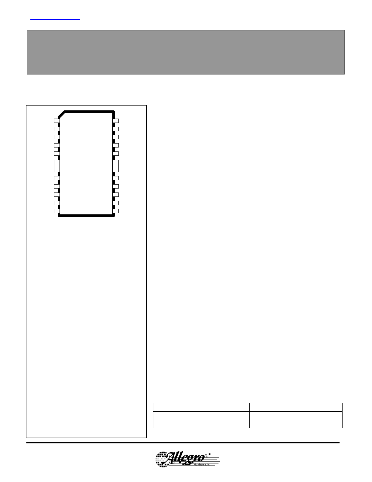
3976
DUAL FULL BRIDGE
PROTECTED MOTOR DRIVER
ENABLE1
PHASE1
GROUND
GROUND
OUT1A
FAULT1
OUT1B
1
V
BB
2
3
4
n/c
5
n/c
A3976KLB
6
7
8
n/c
9
10
n/c
11
12
24
23
22
21
20
19
18
17
16
15
14
13
V
CC
ENABLE2
PHASE2
n/c
n/c
GROUND
GROUND
n/c
OUT2A
n/c
FAULT2
OUT2B
ABSOLUTE MAXIMUM RATINGS
at TA = +25°C
Operating Supply Voltage, VBB....................30 V
Non-Operating Supply Voltage.....................35 V
Output Current, I
Logic Supply Voltage, VCC..........................7.0 V
Fault Output Voltage ...................................7.0 V
Logic Input Voltage Range,
VIN..........................-0.3 V to V
Package Power Dissipation (TA = +25°C), P
A3976KLB..................................2.2 W
A3976KB....................................2.9 W
Operating Temperature Range,
TA..............................-40°°C to +125°°C
Junction Temperature, TJ.........................+150°°C
Storage Temperature Range,
TS...............................-55°°C to +150°°C
* Output current rating may be limited by duty cycle,
ambient temperature, and heat sinking. Under any set of
conditions, do not exceed the specified current rating or a
junction temperature of 150°C.
............................±±500 mA*
OUT
CC
+ 0.3 V
D
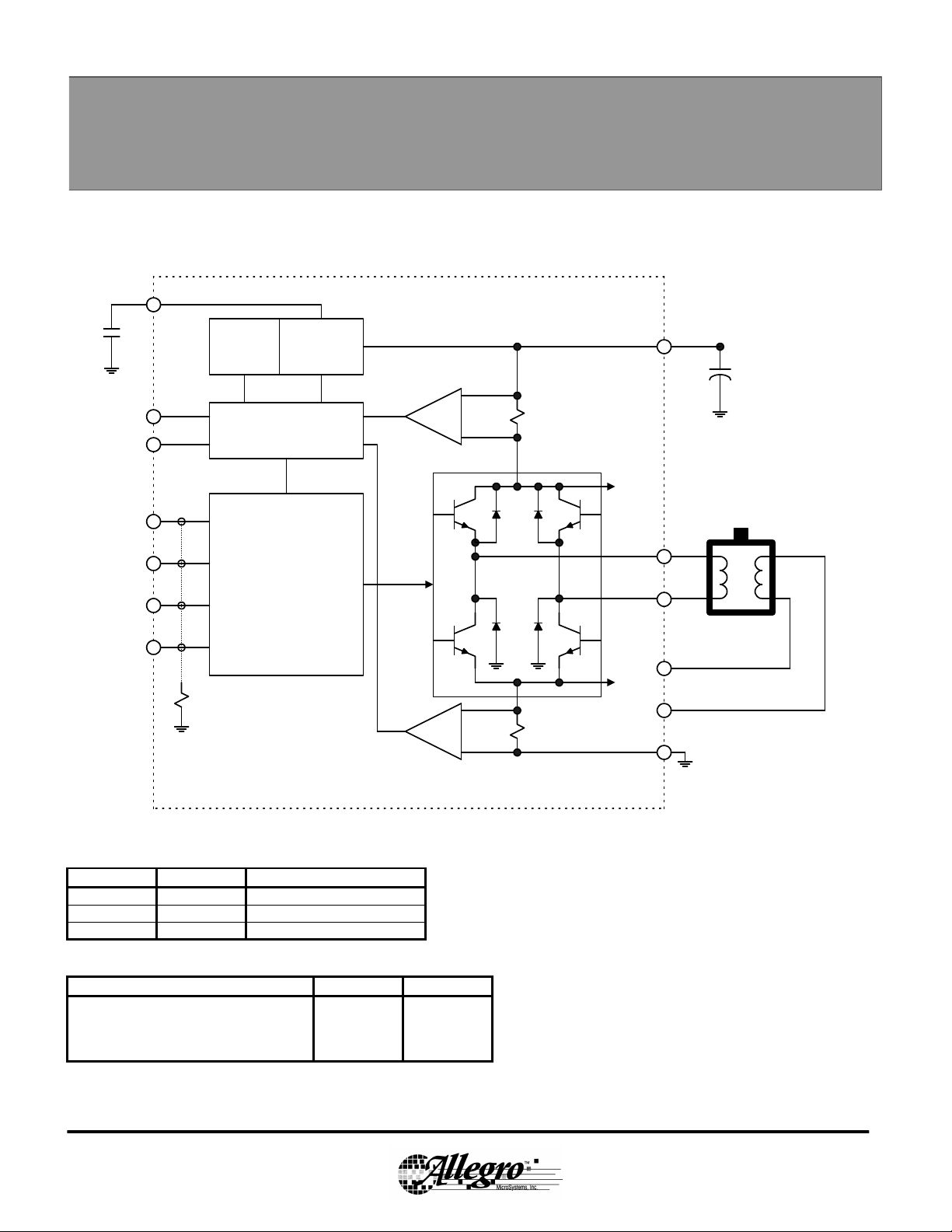
The A3976 is designed to drive both windings of a bipolar stepper
motor or bidirectionally control two DC Motors. Both H-Bridges are capable
of continuous output currents of up to +/- 500 mA and operating voltages to
30V. Free wheeling, substrate isolated diodes are included for output transient
suppression when switching motors or other inductive loads. For each bridge
the PHASE input controls load current polarity by selecting the appropriate
source and sink driver pair. The ENABLE input, when held high, enables the
respective output H-bridge. When both ENABLE pins are held low the device
will enter SLEEP mode and consume less than 100µA.
The 3976 is protected to ensure safe operation in harsh operating
environments and was designed specifically for automotive applications.
Protection circuitry will check for open or shorted load, motor lead short to
ground or supply, VBB overvoltage, VCC undervoltage, and thermal
shutdown. If any of these conditions are detected the outputs will be disabled
and fault information will be output to diagnostic pins FAULT1 and FAULT2.
The 3976 is supplied in a choice of two power packages, a 16-lead
plastic DIP with a copper batwing tab (suffix ‘B’), and a 24-lead plastic SOIC
with a copper batwing tab (suffix ‘LB’). In both cases, the power tab is at
ground potential and needs no electrical isolation.
FEATURES
n 30 V , ±500 mA Continuous Output Rating
n 35V Load Dump Survival
n Output Short Circuit Protection
n Coded Fault Diagnostic Outputs
n Low Current Standby Mode
n Open Load Monitor
n Low Current Standby Mode
n VBB Over Voltage Shutdown
n Internal Thermal Shutdown Circuitry
n Internal Low Parasitic Free Wheeling Diodes
n Crossover Current Protection
PART NUMBER PACKAGE R
ØJA
A3976KLB 24 Lead SOIC 56°°C/W 6°°C/W
A3973KB 16 Lead DIP 43 °°C/W 6°°C/W
R
ØJT
Page 2
Page 2 of 5
3976 Dual Protected PWM Motor Driver
Functional Block Diagram
(one of two bridges shown)
V
CC
FAULT1
FAULT2
PHASE1
ENABLE1
PHASE2
ENABLE2
Thermal
Shutdown
Diagnostic Logic
Input Pull Down
Over/Under
Voltage
Monitor
CONTROL
LOGIC
Short to Supply
Monitor
Short to Ground
Monitor
To Bridge 2
To Bridge 2
V
BB
OUT1A
OUT1B
OUT2A
OUT2B
GROUND
Input Logic
PHASE ENABLE OUTA OUTB
X 0 Off Off
0 1 Low High
1 1 High Low
Fault Logic
Fault Condition FAULT1 FAULT2
Thermal Shutdown Low Low
Short to Battery or Open Load Low High
Short to Ground High Low
Normal Operation High High
Page 3

Page 3 of 5
3976 Dual Protected PWM Motor Driver
ELECTRICAL CHARACTERISTICS at TA = -40 °C to +125°C, VBB = 30 V, VCC = 5.0 V (Unless noted otherwise)
Limits
Characteristics Symbol Test Conditions Min. Typ. Max. Units
Output Drivers
Load Supply Voltage Range V
Logic Supply Range V
Output Current Limit I
Output Leakage Current I
Output Saturation Voltage V
CE(SAT)
Clamp Diode Forward Voltage V
(Flyback or Ground Clamp)
BB
CC
CL
CEX
F
Operating 6 – 30 V
Operating 4.5 5.5 V
Outputs A or B = GROUND 0.7 1.1 – A
Outputs A or B = V
V
= V
BB
= 0 V
V
OUT
OUT
Source Driver, I
Source Driver, I
Sink Driver, I
Sink Driver, I
BB
= -350 mA
OUT
= -500 ma – 1.2 1.3
OUT
= +350 mA
OUT
= +500 ma – 0.4 0.6 V
OUT
IF = 500 mA (Sink / Ground Clamp)
IF = 500 mA (Source / Flyback)
0.7 1.1 – A
– <1.0 50 µA
– <1.0 -50 µA
– 1.0 1.2 V
– 0.2 0.4 V
– 1.2 1.5 V
– 1.55 2.0 V
Control Logic
Motor Supply Current I
BB
ENABLE1 = ENABLE2 = High – 7 10 mA
(No Load) Sleep Mode ENABLE1 = ENABLE2 = Low – – 25 µA
Logic Supply Current I
CC
ENABLE1 = ENABLE2 = High – 45 50 MA
Logic Input Voltage
Logic Input Current
V
V
I
I
IN(1)
IN(0)
IN(1)
IN(0)
Sleep Mode, ENABLE1 = ENABLE2 = Low – – 75 µA
0.7V
– – .3V
– - V
CC
CC
VIN = 5 V – 50 100 µA
VIN = 0V – -1.0 -2.0 µA
V
Page 4

Page 4 of 5
3976 Dual Protected PWM Motor Driver
ELECTRICAL CHARACTERISTICS at TA = -40°C +125°C, VBB = 30 V, VDD = 5.0 V (unless noted otherwise)
Limits
Characteristics Symbol Test Conditions Min. Typ. Max. Units
Fault Circuitry
Fault Output Leakage I
F-LEAK
Fault Output Low V
Fault Output Current I
Output Open Load Current I
OUT-O.L.
Thermal Fault Temp. T
Thermal Fault Hysteresis T
FL
F
F
FHYS
VF = 5 Volts, No Faults - - 10 µA
Fault Condition Asserted, IF=25 µA – 0.8 V
VF = 5 Volts, ENABLE=3.5V 25 50 75 µA
V
= 12 V – 2 – mA
BB
– 170 – °C
– 10 – °C
OVLO Enable Threshold Vbb rising 27 30 33 V
OVLO Hysteresis 1.5 V
UVLO Enable Threshold Vcc falling 3.5 4 4.5 V
UVLO Hysteresis – 400 – mV
Timing
Open Fault to Reset Delay t
PHASE_X Delay to OPEN Fault t
PHASE_X Delay to S.C. Fault t
ENABLE_X Delay to Fault t
Propagation Delay Times
rs
of
SC
of
t
pd
V
= 12 V – – 25 µs
BB
V
= 12 V – 30 – µs
BB
V
= 12 V – 5 – µs
BB
V
= 12 V – 5 – µs
BB
I
= ±0.35A, 50%TO 90%
OUT
Cross Over Dead Time t
CODT
ENABLE ON TO SOURCE ON – 0.3 µs
ENABLE OFF TO SOURCE OFF – 0.4 µs
ENABLE ON TO SINK ON – 0.3 µs
ENABLE OFF TO SINK OFF – 0.2 µs
PHASE CHANGE TO SINK ON – 4.0 µs
PHASE CHANGE TO SINK OFF – 0.3 µs
PHASE CHANGE TO SOURCE ON – 4.0 µs
PHASE CHANGE TO SOURCE OFF – 0.4 µs
1KΩ (1k+1k) Load (VBB to OUT to GND) 0.5 3.0 6.0 µs
Page 5

Page 5 of 5
3976 Dual Protected PWM Motor Driver
APPLICATION NOTES
Open Lead Protection. During normal PWM
operation diagnostic circuitry will look for a minimum
source current level after a bridge is signalled on.
Additionally, the diode flyback is monitored on the proper
output. The logic will signal a fault and disable the outputs if
it determines that the current is below the minimum level
AND no flyback is occurring. If the inductive load is too
large, the current would take too long to reach the minimal
level and a false open load would be reported. It is
recommended that the inductive load be less than 38mH.
Short Circuit Protection. Internal sense resistors in
series with VBB and ground will trip the fault circuitry if
greater than 1.1A is detected. To prevent false overcurrent
events due to reverse recovery spikes of the clamp diodes,
the current monitor is blanked for 5us after a high side is
signalled to turn on. If an additional input command follows
after the initial fault, the selected pair of drivers will pulse on
for the 5us blanking duration. The short circuit fault will
remember the input state where the fault occurred and will
wait for that particular logic state after the short has been
removed before normal operation is allowed to resume.
Thermal Protection. Circuitry turns OFF all drivers
when the junction temperature reaches 170°C typically. It is
intended only to protect the device from failures due to
excessive junction temperatures and has a hysteresis of
approximately 15°C.
Layout. The printed wiring board should use a heavy
ground plane. For optimum electrical and thermal
performance, the driver should be soldered directly onto the
board. The load supply pin, VBB, should be decoupled with
an electrolytic capacitor (> 47 µF is recommended) placed as
close to the device as possible.
Terminal List
Pin Name Pin Description 24 Lead SOIC 16 Lead DIP
V
BB
ENABLE1 Control Logic – Bridge 1 2 2
PHASE1 Control Logic – Bridge 1 3 3
GROUND Power Ground Return 18,19,6,7 4,5,12,13
OUT1A Bridge 1 Output 9 6
FAULT1 Diagnostic Output 11 7
OUT1B Bridge 1 Output 12 8
OUT2B Bridge 2 Output 13 9
FAULT2 Diagnostic Output 14 10
OUT2A Bridge 2 Output 16 11
PHASE2 Control Logic – Bridge 2 22 14
ENABLE2 Control Logic – Bridge 2 23 15
V
CC
NC No Connect 3,4,5,8,15,17,20,21
Motor Supply Voltage 1 1
Logic Supply 24 16
 Loading...