

Page 1
查询A3958SB-T供应商
3958
DMOS FULL-BRIDGE PWM
29319.31B
MOTOR DRIVER
Data Sheet
A3958SLB
24
V
RANGE
23
NO
22
CONNECTION
21
OUT
20
LOAD SUPPLY
19
GROUND
18
GROUND
SENSE
17
OUTA
16
NO
15
CONNECTION
MODE
14
REF
13
REG
B
Dwg. PP-069A
CP
CP1
PHASE
OSC
GROUND
GROUND
LOGIC SUPPLY
ENABLE
DATA
CLOCK
STROBE
CP
1
2
2
LOGIC
NC
V
BB
NC
÷
3
4
5
6
7
8
9
9
10
11
12
θ
V
DD
CHARGE PUMP
SERIAL PORT
Note that the A3958SLB(SOIC) and A3958SB
(DIP) do not share a common terminal
assignment.
ABSOLUTE MAXIMUM RATINGS
Load Supply Voltage, VBB...................... 50 V
Output Current, I
Logic Supply Voltage, VDD.................... 7.0 V
Input Voltage, VIN....... -0.3 V to VDD + 0.3 V
Sense Voltage, VS................................... 0.5 V
Reference Voltage, V
Package Power Dissipation (TA = 25°C), P
A3958SB ...................................... 3.1 W*
A3958SLB .................................... 1.6 W*
Operating Temperature Range,
TA.................................... -20°C to +85°C
Junction Temperature,
TJ.................................................. +150°C
Storage Temperature Range,
TS.................................. -55°C to +150°C
Output current rating may be limited by duty cycle,
ambient temperature, and heat sinking. Under any
set of conditions, do not exceed the specified
current rating or a junction temperature of 150°C.
* Per SEMI G42-88 Specification.
............................. ±2.0 A
OUT
........................ 2.7 V
REF
D
Designed for pulse-width modulated (PWM) current control of dc
motors, the A3958SB and A3958SLB are capable of continuous output
currents to ±2 A and operating voltages to 50 V. Internal fixed offtime PWM current-control timing circuitry can be programmed via a
serial interface to operate in slow, fast, and mixed current-decay
modes.
PHASE and ENABLE input terminals are provided for use in
controlling the speed and direction of a dc motor with externally
applied PWM-control signals. The ENABLE input can be
programmed via the serial port to PWM the bridge in fast or slow
current decay. Internal synchronous rectification control circuitry is
provided to reduce power dissipation during PWM operation.
Internal circuit protection includes thermal shutdown with
hysteresis, and crossover-current protection. Special power-up
sequencing is not required.
The A3958SB/SLB is supplied in a choice of two power
packages, a 24-pin plastic DIP with a copper batwing tab (package
suffix ‘B’), and a 24-pin plastic SOIC with a copper batwing tab
(package suffix ‘LB’). In both cases, the power tab is at ground
potential and needs no electrical isolation. Each package type is
available in a lead-free version (100% matte tin leadframe).
FEATURES
±2 A, 50 V Continuous Output Rating
Low r
Outputs (270 mΩ, Typical)
DS(on)
Programmable Mixed, Fast, and Slow Current-Decay Modes
Serial Interface Controls Chip Functions
Synchronous Rectification for Low Power Dissipation
Internal UVLO and Thermal-Shutdown Circuitry
Crossover-Current Protection
Always order by complete part number:
Part Number Package R
A3958SB 24-pin batwing DIP 40°C/W 6°C/W
A3958SB-T 24-pin batwing DIP; Lead-free 40°C/W 6°C/W
A3958SLB 24-lead batwing SOIC 77°C/W 6°C/W
A3958SLB-T 24-lead batwing SOIC; Lead-free 77°C/W 6°C/W
† See also, Layout, page 8.
†R
θθ
θJA
θθ
θθ
θJT
θθ
Page 2
3958
DMOS FULL-BRIDGE
PWM MOTOR DRIVER
V
DD
LOGIC
SUPPLY
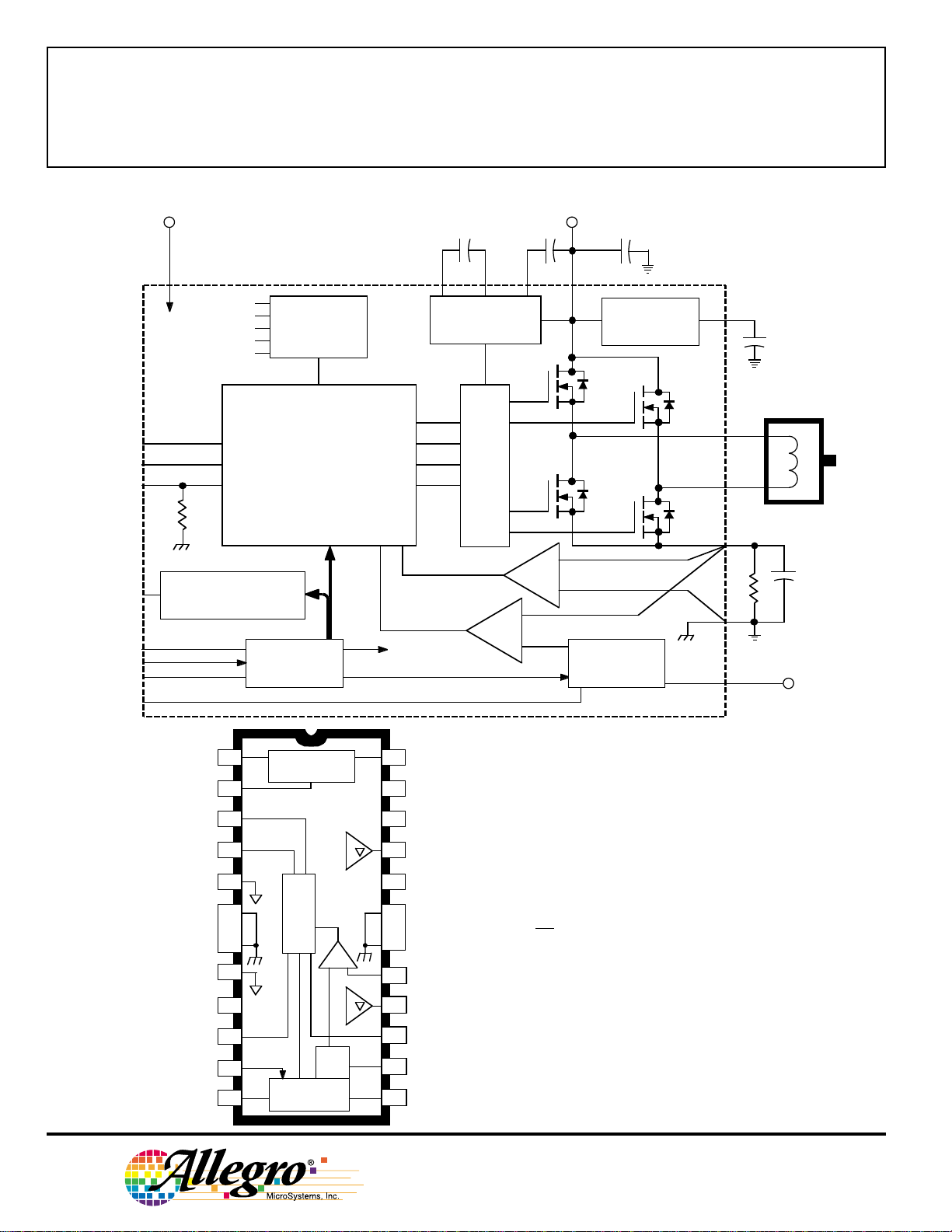
FUNCTIONAL BLOCK DIAGRAM
V
BB
CP1
CP2
CP
LOAD
SUPPLY
+
MODE
PHASE
ENABLE
OSC
CLOCK
DATA
STROBE
RANGE
CHARGE PUMP
BANDGAP
V
DD
C
REG
TSD
PROGRAMMABLE
PWM TIMER
UNDER-
VOLTAGE &
FAULT DETECT
CONTROL LOGIC
PHASE
ENABLE
FIXED OFF
BLANK
DECAY
SERIAL
PORT
SYNC RECT MODE
SYNC RECT DISABLE
PWM MODE INT
PWM MODE EXT
SLEEP
MODE
CHARGE
PUMP
GATE DRIVE
CURRENT
SENSE
ZERO
CURRENT
DETECT
RANGE
BANDGAP
REGULATOR
REFERENCE
BUFFER &
DIVIDER
V
REG
OUT
OUT
SENSE
REF
A
B
R
C
S
S
Dwg. FP-048
REF
V
2
1
CHARGE PUMP
CP
1
2
PHASE
OSC
GROUND
GROUND
GROUND
GROUND
LOGIC
SUPPLY
ENABLE
DATA
CLOCK
θ
3
4
5
6
7
8
9
V
9
DD
10
11
12
LOGIC
SERIAL PORT
V
BB
÷
2
CPCP
24
REG
V
23
RANGE
22
21
OUT
B
20
19
18
17
16
15
14
13
Dwg. PP-069-1A
LOAD
SUPPLY
GROUND
GROUND
SENSE
OUT
MODE
REF
STROBE
A3958SB
Note that the A3958SLB (SOIC) and A3958SB
(DIP) do
assignment.
A
not share a common terminal
115 Northeast Cutoff, Box 15036
Worcester, Massachusetts 01615-0036 (508) 853-5000
Copyright © 2000, 2002 Allegro MicroSystems, Inc.
Page 3

3958
DMOS FULL-BRIDGE
PWM MOTOR DRIVER
ELECTRICAL CHARACTERISTICS at T
f
< 50 kHz (unless noted otherwise)
PWM
= +25°C, V
A
= 50 V, VDD = 5.0 V, V
BB
SENSE
= 0.5 V,
Limits
Characteristics Symbol Test Conditions Min. Typ. Max. Units
Output Drivers
Load Supply Voltage Range V
BB
Operating 20 – 50 V
During sleep mode 0 – 50 V
Output Leakage Current I
Output On Resistance r
DS(on)
Body Diode Forward Voltage V
DSS
V
= V
OUT
V
OUT
Source driver, I
Sink driver, I
Source diode, IF = -2 A – 1.2 1.6 V
F
BB
= 0 V – <-1.0 -20 µA
= -2 A – 270 300 mΩ
OUT
= 2 A – 270 300 mΩ
OUT
– <1.0 20 µA
Sink diode, IF = 2 A – 1.2 1.6 V
Load Supply Current I
BB
f
< 50 kHz – 4.0 7.0 mA
PWM
Charge pump on, outputs disabled – 2.0 5.0 mA
Sleep Mode – – 20 µA
Control Logic
Logic Supply Voltage Range V
Logic Input Voltage V
V
Logic Input Current I
(all inputs except ENABLE)
ENABLE Input Current I
OSC input frequency f
OSC input duty cycle dc
IN(1)
IN(0)
IN(1)
I
IN(0)
IN(1)
I
IN(0)
OSC
DD
OSC
Operating 4.5 5.0 5.5 V
2.0 – – V
– – 0.8 V
V
= 2.0 V – <1.0 20 µA
IN
V
= 0.8 V – <-2.0 -20 µA
IN
V
= 2.0 V – 40 100 µA
IN
V
= 0.8 V – 16 40 µA
IN
Operating 2.9 – 6.1 MHz
Operating 40 – 60 %
OSC input hysteresis – Operating 200 – 400 mV
Input Hysterisis – All digital inputs except OSC 50 – 100 mV
Reference Input Volt. Range V
Reference Input Current I
Comparator Input Offset Volt. V
REF
REF
IO
Operating 0.0 – 2.6 V
V
= 2.5 V – – ±0.5 µA
REF
V
= 0 V – 0 ±5.0 mV
REF
Continued next page …
www.allegromicro.com
3
Page 4

3958
DMOS FULL-BRIDGE
PWM MOTOR DRIVER
ELECTRICAL CHARACTERISTICS at T
f
< 50 kHz (unless noted otherwise), continued.
PWM
= +25°C, V
A
= 50 V, VDD = 5.0 V, V
BB
SENSE
= 0.5 V,
Limits
Characteristics Symbol Test Conditions Min. Typ. Max. Units
Control Logic
Buffer Input Offset Volt. V
IO
–0±15 mV
Reference Divider Ratio – D14 = High 9.9 10 10.2 –
D14 = Low 4.95 5.0 5.05 –
Propagation Delay Times t
pd
PWM change to source ON – 600 – ns
PWM change to source OFF – 100 – ns
PWM change to sink ON – 600 – ns
PWM change to sink OFF – 100 – ns
Phase change to sink ON – 600 – ns
Phase change to sink OFF – 100 – ns
Phase change to source ON – 600 – ns
Phase change to source OFF – 100 – ns
Thermal Shutdown Temp. T
Thermal Shutdown Hysteresis ∆T
J
J
UVLO Enable Threshold UVLO Increasing V
DD
– 165 – °C
–15– °C
3.90 4.2 4.45 V
UVLO Hysteresis ∆UVLO 0.05 0.10 – V
Logic Supply Current I
DD
f
< 50 kHz – 6.0 10 mA
PWM
Sleep Mode, Inputs < 0.5 V – – 2.0 mA
NOTES: 1. Typical Data is for design information only.
2. Negative current is defined as coming out of (sourcing) the specified device terminal.
4
115 Northeast Cutoff, Box 15036
Worcester, Massachusetts 01615-0036 (508) 853-5000
Page 5

FUNCTIONAL DESCRIPTION
3958
DMOS FULL-BRIDGE
PWM MOTOR DRIVER
Serial Interface. The A3958 is controlled via a 3-wire
(clock, data, strobe) serial port. The programmable
functions allow maximum flexibility in configuring the
PWM to the motor drive requirements. The serial data is
clocked in starting with D19.
Bit Function
D0 Blank Time LSB
D1 Blank Time MSB
D2 Off Time LSB
D3 Off Time Bit 1
D4 Off Time Bit 2
D5 Off Time Bit 3
D6 Off Time MSB
D7 Fast Decay Time LSB
D8 Fast Decay Time Bit 1
D9 Fast Decay Time Bit 2
D10 Fast Decay Time MSB
D11 Sync. Rect. Mode
D12 Sync. Rect. Enable
D13 External PWM Mode
D14 Enable
D15 Phase
D16 Reference Range Select
D17 Internal PWM Mode
D18 Test Use Only
D19 Sleep Mode
D0 – D1 Blank Time. The current-sense comparator is
blanked when any output driver is switched on, according
to the table below. f
is the oscillator input frequency.
osc
D1 D0 Blank Time
0 0 4/f
0 1 6/f
1 0 12/f
1 1 24/f
osc
osc
osc
osc
D2 – D6 Fixed-Off Time. A five-bit word sets the
fixed-off time for internal PWM current control. The off
time is defined by
t
= (8[1 + N]/f
off
osc
) - 1/f
osc
where N = 0 … 31
For example, with an oscillator frequency of 4 MHz, the
off time will be adjustable from 1.75 µs to 63.75 µs in
increments of 2 µs.
D7 – D10 Fast Decay Time. A four-bit word sets the
fast-decay portion of the fixed-off time for the internal
PWM control circuitry. This will only have impact if the
mixed-decay mode is selected (via bit D17 and the MODE
input terminal). For t
fd
> t
, the device will effectively
off
operate in the fast-decay mode. The fast decay portion is
defined by
t
= (8[1 + N]/f
fd
osc
) - 1/f
osc
where N = 0 … 15
For example, with an oscillator frequency of 4 MHz, the
fast decay time will be adjustable from 1.75 µs to
31.75 µs in increments of 2 µs.
D11 Synchronous Rectification Mode. The active
mode prevents reversal of load current by turning off
synchronous rectification when a zero current level is
detected. The passive mode will allow reversal of current
but will turn off the synchronous rectifier circuit if the
load current inversion ramps up to the current limit set by
V
REF/RS
.
D11 Mode
0 Active
1 Passive
D12 Synchronous Rectification Enable.
D12 Synchronous Rect.
0 Disabled
1 Enabled
D13 External PWM Decay Mode. Bit D13 determines
the current-decay mode when using ENABLE chopping
for external PWM current control.
D13 Mode
0 Fast
1 Slow
D14 Enable Logic. Bit D14, in conjunction with
ENABLE, determines if the output drivers are in the
chopped (OFF)(ENABLE = D14) or ON (ENABLE ≠
D14) state.
ENABLE D14 Mode
0 0 Chopped
10On
01On
1 1 Chopped
www.allegromicro.com
5
Page 6

3958
DMOS FULL-BRIDGE
PWM MOTOR DRIVER
FUNCTIONAL DESCRIPTION (continued)
D15 Phase Logic. Bit D15, in conjunction with
PHASE, determines if the device is operating in the
forward (PHASE ≠ D15) or reverse (PHASE = D15) state.
PHASE D15 State OUTAOUT
B
0 0 Reverse Low High
1 0 Forward High Low
0 1 Forward High Low
1 1 Reverse Low High
D16 G
RANGE, determines if V
Range Select. Bit D16, in conjunction with
m
is divided by 5 (RANGE ≠
REF
D16) or by 10 (RANGE = D16).
RANGE D16 Divider
00÷10
10÷5
01÷5
11÷10
D17 Internal PWM Mode. Bit D17, in conjunction with
MODE, selects slow (MODE ≠ D17) or mixed (MODE =
D17) current decay.
MODE D17
Current-Decay Mode
0 0 Mixed
1 0 Slow
0 1 Slow
1 1 Mixed
D18 Test Mode. Bit D18 low (default) operates the
device in normal mode. D18 is only used for testing
purposes. The user should never change this bit.
D19 Sleep Mode. Bit D19 selects a Sleep mode to
minimize power consumption when not in use. This
disables much of the internal circuitry including the
regulator and charge pump. On power up the serial port is
initialized to all 0s. Bit D19 should be programmed high
for 1 ms before attempting to enable any output driver.
D19 Sleep Mode
0 Sleep
1 Normal
Serial Port Write Timing Operation. Data is clocked
into the shift register on the rising edge of the CLOCK
signal. Normally STROBE will be held high, only
brought low to initiate a write cycle. Refer to diagram
below and these specifications for the minimum timing
requirements.
A.DATA setup time ......................................... 15 ns
B.DATA hold time ........................................... 10 ns
C.Setup STROBE to CLOCK rising edge ....... 50 ns
D.CLOCK high pulse width ............................ 50 ns
E.CLOCK low pulse width .............................. 50 ns
F.Setup CLOCK rising edge to STROBE ....... 50 ns
G.STROBE pulse width ................................... 50 ns
Serial Port Write Timing
STROBE
E
CLOCK
A
DATA
6
B
D19 D0D18
115 Northeast Cutoff, Box 15036
Worcester, Massachusetts 01615-0036 (508) 853-5000
F
GC D
Dwg. WP-038
Page 7

DMOS FULL-BRIDGE
PWM MOTOR DRIVER
FUNCTIONAL DESCRIPTION (continued)
3958
V
. This internally generated voltage is used to operate
REG
the sink-side DMOS outputs. The V
be decoupled with a 0.22 µF capacitor to ground. V
terminal should
REG
REG
is
internally monitored and in the case of a fault condition,
the outputs of the device are disabled.
Charge Pump. The charge pump is used to generate a
gate-supply voltage greater than V
to drive the source-
BB
side DMOS gates. A 0.22 µF ceramic capacitor should be
connected between CP1 and CP2 for pumping purposes.
A 0.22 µF ceramic capacitor should be connected between
CP and V
to act as a reservoir to operate the high-side
BB
DMOS devices. The CP voltage is internally monitored
and, in the case of a fault condition, the source outputs of
the device are disabled.
Shutdown. In the event of a fault (excessive junction
temperature, or low voltage on CP or V
) the outputs of
REG
the device are disabled until the fault condition is
removed. At power up, and in the event of low V
DD
, the
UVLO circuit disables the drivers and resets the data in
the serial port to all zeros.
PWM Timer Function. The PWM timer is
programmable via the serial port (bits D2 – D10) to
provide off-time PWM signals to the control circuitry. In
the mixed current-decay mode, the first portion of the off
time operates in fast decay, until the fast decay time count
(serial bits D7 – D10) is reached, followed by slow decay
for the rest of the off-time period (bits D2 – D6). If the
fast decay time is set longer than the off time, the device
effectively operates in fast decay mode. Bit D17, in
conjunction with MODE, selects mixed or slow decay.
PWM Blank Timer. When a source driver turns on, a
current spike occurs due to the reverse recovery currents
of the clamp diodes and/or switching transients related to
distributed capacitance in the load. To prevent this current
spike from erroneously resetting the source-enable latch,
the sense comparator is blanked. The blank timer runs
after the off-time counter (see bits D2 – D6) to provide the
programmable blanking function. The blank timer is reset
when ENABLE is chopped or PHASE is changed. For
external PWM control, a PHASE change or ENABLE on
will trigger the blanking function.
Synchronous Rectification. When a PWM off cycle
is triggered, either by an ENABLE chop command or
internal fixed off-time cycle, load current will recirculate
according to the decay mode selected by the control logic.
The A3958 synchronous rectification feature will turn on
the opposite pair of DMOS outputs during the current
decay and effectively short out the body diodes with the
low r
driver. This will reduce power dissipation
DS(on)
significantly and can eliminate the need for external
Schottky diodes.
Synchronous rectification can be configured in active
mode, passive mode, or disabled via the serial port (bits
D11 and D12).
The active or passive mode selection has no impact in
slow-decay mode. With synchronous rectification
enabled, the slow-decay mode serves as an effective brake
mode.
Current Regulation. Load current is regulated by an
internal fixed off-time PWM control circuit. When the
outputs of the DMOS H bridge are turned on, the current
increases in the motor winding until it reaches a trip value
determined by the external sense resistor (R
analog reference voltage (V
), the RANGE logic level,
REF
), the applied
S
and serial data bit D16:
When RANGE = D16 ........... I
When RANGE ≠ D16 ............ I
TRIP
TRIP
= V
= V
REF
REF
/10R
/5R
S
S
At the trip point, the sense comparator resets the sourceenable latch, turning off the source driver. The load
inductance then causes the current to recirculate for the
serial-port-programmed fixed off-time period. The
current path during recirculation is determined by the
configuration of slow/mixed current-decay mode (D17)
and the synchronous rectification control bits (D11 and
D12).
www.allegromicro.com
7
Page 8

3958
DMOS FULL-BRIDGE
PWM MOTOR DRIVER
APPLICATIONS INFORMATION
Current Sensing. To minimize inaccuracies in sensing
the I
current level, which may be caused by ground
TRIP
trace IR drops, the sense resistor should have an
independent ground return to the ground terminal of the
device. For low-value sense resistors the IR drops in the
PCB sense resistor’s traces can be significant and should
be taken into account. The use of sockets should be
avoided as they can introduce variation in R
due to their
S
contact resistance.
The maximum value of R
is given as RS ≤ 0.5/I
S
TRIP
.
Braking. The braking function is implemented by
driving the device in slow-decay mode via serial port bit
D13, enabling synchronous rectification via bit D12, and
chopping with the combination of D14 and the ENABLE
input terminal. Because it is possible to drive current in
either direction through the DMOS drivers, this
configuration effectively shorts out the motor-generated
BEMF as long as the ENABLE chop mode is asserted. It
is important to note that the internal PWM current-control
circuit will not limit the current when braking, because the
current does not flow through the sense resistor. The
maximum brake current can be approximated by V
R
. Care should be taken to ensure that the maximum
L
BEMF
/
ratings of the device are not exceeded in worst-case
braking situations of high speed and high inertial loads.
Layout. The printed wiring board should use a heavy
ground plane. For optimum electrical and thermal performance*, the driver should be soldered directly onto the
board. The ground side of R
should have an individual
S
path to the ground terminals of the device. This path
should be as short as is possible physically and should not
have any other components connected to it. It is recommended that a 0.1 µF capacitor be placed between SENSE
and ground as close to the device as possible; the load
supply terminal, V
, should be decoupled with an
BB
electrolytic capacitor (> 47 µF is recommended) placed as
close to the device as is possible.
* The thermal resistance and absolute maximum allowable
package power dissipation specified on page 1 is measured on typical two-sided PCB with minimal copper
ground area. See also, Application Note 29501.5, Improv-
ing Batwing Power Dissipation. For example, for the
‘LB’ package (SOIC), R
with 3.57 in
5
4
2
copper ground area
can be reduced to 49°C/W
θJA
R = 6.0°C/W
θJT
Thermal Protection. Circuitry turns off all drivers
when the junction temperature reaches 165°C typically. It
is intended only to protect the device from failures due to
excessive junction temperatures and should not imply that
output short circuits are permitted. Thermal shutdown has
a hysteresis of approximately 15°C.
8
115 Northeast Cutoff, Box 15036
Worcester, Massachusetts 01615-0036 (508) 853-5000
3
SUFFIX 'B', R = 40°C/W
2
1
SUFFIX 'LB', R = 77°C/W
0
25
ALLOWABLE PACKAGE POWER DISSIPATION IN WATTS
50 75 100 125 150
TEMPERATURE IN °°°°C
θJA
θJA
Dwg. GP-049B
Page 9

3958
DMOS FULL-BRIDGE
PWM MOTOR DRIVER
Terminal List
A3958SLB A3958SB
Terminal Name Terminal Description (SOIC) (DIP)
CP Reservoir capacitor (typically 0.22 µF) 1 24
CP1 & CP2 The charge pump capacitor (typically 0.22 µF) 2 & 3 1 & 2
PHASE Logic input for direction control (see also D15) 4 3
OSC Logic-level oscillator (square wave) input 5 4
GROUND Grounds 6, 7 5, 6, 7, 8*
LOGIC SUPPLY V
, the low voltage (typically 5 V) supply 8 9
DD
ENABLE Logic input for enable control (see also D14) 9 10
DATA Logic-level input for serial interface 10 11
CLOCK Logic input for serial port (data is entered on rising edge) 11 12
STROBE Logic input for serial port (active on rising edge) 12 13
REF V
, the load current reference input volt. (see also D16) 13 14
REF
MODE Logic input for PWM mode control (see also D17) 14 15
NO CONNECT No (Internal) Connection 15 —
OUT
A
One of two DMOS bridge outputs to the motor 16 16
SENSE Sense resistor 17 17
GROUND Grounds 18, 19 18, 19*
LOAD SUPPLY V
OUT
B
, the high-current, 20 V to 50 V, motor supply 20 20
BB
One of two DMOS bridge outputs to the motor 21 21
NO CONNECT No (Internal) connection 22 —
RANGE Logic Input for V
V
REG
Regulator decoupling capacitor (typically 0.22 µF) 24 23
range control (see also D16) 23 22
REF
* For the A3958SB DIP only, there is an indeterminate resistance between the substrate grounds (pins 6, 7, 18,
and 19) and the grounds at pins 5 and 8. Pins 5 and 8, and 6, 7, 18, or 19 must be connected together externally.
www.allegromicro.com
9
Page 10

3958
DMOS FULL-BRIDGE
PWM MOTOR DRIVER
24
0.280
0.240
NOTE 1
A3958SB
Dimensions in Inches
(controlling dimensions)
13
0.014
0.008
0.300
BSC
0.430
MAX
0.210
MAX
7.11
6.10
0.015
MIN
16
0.070
0.045
0.022
0.014
24
1
1.77
1.15
7
NOTE 1
67
12
1.280
1.230
0.100
BSC
Dimensions in Millimeters
(for reference only)
13
12
32.51
31.24
2.54
BSC
0.005
0.150
0.115
0.13
MIN
MIN
0.355
0.204
Dwg. MA-001-25A in
10.92
MAX
7.62
BSC
5.33
MAX
0.39
MIN
0.558
0.356
NOTES: 1. Webbed lead frame. Leads 6, 7, 18, and 19 are internally one piece.
2. Exact body and lead configuration at vendor’s option within limits shown.
3. Lead spacing tolerance is non-cumulative.
4. Lead thickness is measured at seating plane or below.
5. Supplied in standard sticks/tubes of 15 devices.
10
115 Northeast Cutoff, Box 15036
Worcester, Massachusetts 01615-0036 (508) 853-5000
3.81
2.93
Dwg. MA-001-25A mm
Page 11

A3958SLB
Dimensions in Inches
(for reference only)
3958
DMOS FULL-BRIDGE
PWM MOTOR DRIVER
0.2992
0.2914
0.020
0.013
0.0926
0.1043
24 13
1 2
3
0.6141
0.5985
0.0040
MIN
.
Dimensions in Millimeters
(controlling dimensions)
24 13
0.050
BSC
NOTE 1
NOTE 3
0.419
0.394
0°
TO
8°
0.0125
0.0091
0.050
0.016
Dwg. MA-008-25A in
0.32
0.23
7.60
7.40
1 2
0.51
0.33
3
15.60
15.20
1.27
BSC
NOTE 1
NOTE 3
2.65
2.35
0.10
MIN
.
NOTES: 1. Exact body and lead configuration at vendor’s option within limits shown.
2. Lead spacing tolerance is non-cumulative.
3. Webbed lead frame. Leads 6, 7, 18, and 19 are internally one piece.
4. Supplied in standard sticks/tubes of 31 devices or add “TR” to part number for tape and reel.
www.allegromicro.com
10.65
10.00
0°
TO
8°
Dwg. MA-008-25A mm
1.27
0.40
11
Page 12

3958
DMOS FULL-BRIDGE
PWM MOTOR DRIVER
12
The products described here are manufactured under one or more
U.S. patents or U.S. patents pending.
Allegro MicroSystems, Inc. reserves the right to make, from time to
time, such departures from the detail specifications as may be
required to permit improvements in the performance, reliability, or
manufacturability of its products. Before placing an order, the user is
cautioned to verify that the information being relied upon is current.
Allegro products are not authorized for use as critical components
in life-support devices or systems without express written approval.
The information included herein is believed to be accurate and
reliable. However, Allegro MicroSystems, Inc. assumes no responsibility for its use; nor for any infringement of patents or other rights of
third parties which may result from its use.
115 Northeast Cutoff, Box 15036
Worcester, Massachusetts 01615-0036 (508) 853-5000
Page 13

 Loading...