

Page 1
358
8-Channel Fault-Protected
Analog Multiplexer
Memory
FEATURES:
•RAD-PAK® technology-hardened against natural space radi-
ation
• Total dose hardness:
- > 50 krad (Si), depending upon space mission
• Excellent Single Event Effect
- SEL
> 80 MeV/mg/cm
TH
- SEUTH > 80 MeV/mg/cm
• Package:
- 16 pin R
• All switches off with power supplies off
• On channel turns OFF if overvoltage occurs
• Only nanoamperes of input current under all fault conditions
• Operates from ±4.5 to ±18V supplies
• All digital inputs are TTL and CMOS compatible
• Significantly reduced power consumption
AD-PAK® Flat Pack
2
2
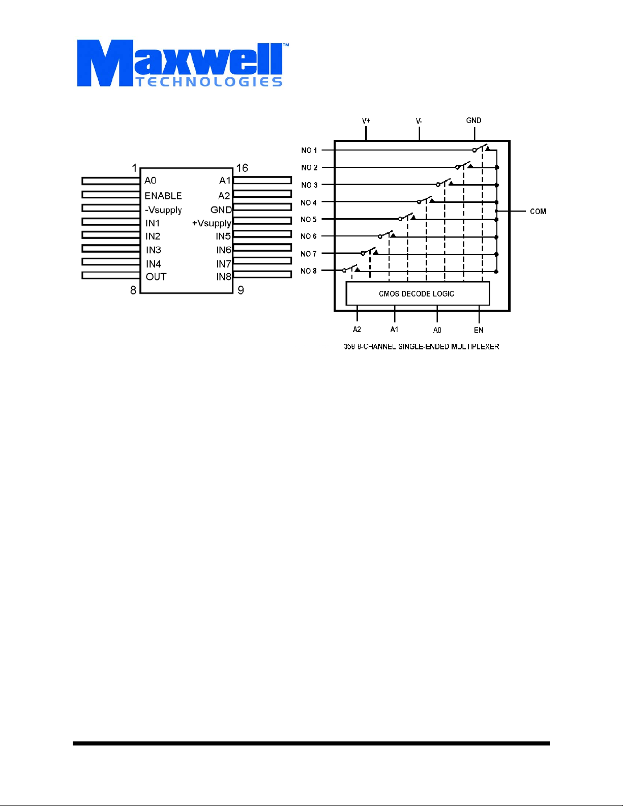
Logic Diagram
DESCRIPTION:
Maxwells’s 358 8-Channel single-ended (1 of 8) multiplexers
with fault protection features a greater than 50 krad (Si) total
dose tolerance, depending upon space mission. Using a
series N-channel, P-channel, N-channel structure, these multiplexers provide significantly improved fault protection. If the
power supplies to the fault-protected multiplexer are inadvertently turned off while input voltages are still applied, all channels in the multiplexer are turned off, and only a few
nanoamperes of leakage current will flow into the inputs. This
protects not only the multiplexer and the circuitry driven by the
multiplexer, but also protects the sensors or signal sources
which drive the multiplexer. All digital inputs have logic thresholds of 0.8V and 2.4V, ensuring both TTL and CMOS compatibility without requiring pullup resistors. Break-before-make
operation is guaranteed. Power supply currents have been
reduced and typical power dissipation is less than 2 mW.
Maxwell Technologies' patented R
ogy incorporates radiation shielding in the microcircuit package. It eliminates the need for box shielding while providing
the required radiation shielding for a lifetime in orbit or a space
mission. In a GEO orbit, Rad-Pak provides true greater than
50 krad (Si) total radiation dose tolerance, dependent upon
space mission. This product is available with packaging and
screening up to Class S.
AD-PAK® packaging technol-
1000544
(858) 503-3000 - Fax: (858) 503-3301 - www.maxwell.com
12.20.01 Rev 2
All data sheets are subject to change without notice
©2001 Maxwell Technologies
All rights reserved.
1
Page 2
8-Channel Fault-Protected Analog Multiplexer
TABLE 1. PINOUT DESCRIPTION
PIN SYMBOL DESCRIPTION
1, 16, 15 A0-A2 Address Inputs
2 Enable Enable Inputs
3 -V Supply Negative Supply Voltage
4-7, 12-9 IN1-IN8 Analog Inputs-bidirectional
8 OUT Output-bidirectional
13 +V Supply Positive Supply Voltage
14 GND Ground
TABLE 2. 358 ABSOLUTE MAXIMUM RATINGS
Parameter Symbol Typ Units
Voltage between Supply Pins
V+
V-
Digital Input Overvoltage
VEN, VA Vsupply (+)
Vsupply (-)
Analog Input Overvoltage with Multiplexer
Power On:
VS Vsupply (+)
Vsupply (-)
Analog Input Overvoltage with Multiplexer
Power Off:
VS Vsupply (+)
Vsupply (-)
Continuous Current
Peak Current
(Pulse at 1 ms, 10% duty cycle max)
Thermal Impedance
Operating Temperature Range: T
Storage Temperature Range: T
Θ
JC
A
S
+44
+22
-22
+4
-4
+20
-20
+35
-35
20
40
2.69 °C/W
-55 to +125 °C
-65 to +150 °C
V
V
V
V
mA
358
Memory
(V+ = 15V, V- = -15V, VAH = 2.4V, VAL = 0.8V, TA = -55 TO +125°C, UNLESS OTHERWISE SPECIFIED)
P
ARAMETER TEST CONDITIONS SYMBOL TEMP MIN TYP MAX UNITS
STATIC
ON Resistance V
1000544
TABLE 3. 358 ELECTRICAL CHARACTERISTICS
= ±10V, IS = ±100µA
D
V
= 0.8V, VAH = 2.4V
AL
12.20.01 Rev 2
r
DS(ON)
+25°C
Full
All data sheets are subject to change without notice
1.2
1.5
1.5
1.8
©2001 Maxwell Technologies
All rights reserved.
kΩ
2
Page 3

8-Channel Fault-Protected Analog Multiplexer
TABLE 3. 358 ELECTRICAL CHARACTERISTICS
(V+ = 15V, V- = -15V, VAH = 2.4V, VAL = 0.8V, TA = -55 TO +125°C, UNLESS OTHERWISE SPECIFIED)
P
ARAMETER TEST CONDITIONS SYMBOL TEMP MIN TYP MAX UNITS
358
OFF Input Leakage Current VS = ±10V, VD = +10V
V
= 0.8V
EN
OFF Output Leakage Current V
ON Channel Leakage Current V
= ±10V, VS = +10V
D
V
= 0.8V
EN
= VD = ±10V
S(ALL)
1
I
S(OFF)
I
D(OFF)
I
VAH = VEN = 2.4V
V
= 0.8V
AL
Analog Signal Range
2
FAULT
Output Leakage Current (with
Overvoltage)
Input Leakage Current (with Over-
1
V
= 0V
D
Analog Overvoltage = ±33V
V
= ±25V, VO = ±10V
IN
1
I
D(OFF)
I
S(OFF)
voltage)
Input Leakage Current (w/ Power
Supplies Off)
V
= ±25V, VEN = VO = 0V
IN
A
= A1 = A2 = OV or 5V
O
I
S(OFF)
INPUT
Input Low Threshold V
Input High Threshold V
Input Leakage Current (High or
V
= 4V or 0V
A
3
Low)
D(ON)
V
AN
AL
AH
I
A
+25°C
Full
+25°C
Full
+25°C
Full
0.03
0.1
0.1
50
200
200
nA
nA
nA
2
Full -15 15 V
+25°C
Full
4.0
2.0
nA
µA
+25°C 5.0 µA
+25°C 2.0 µA
Full 0.8 V
Full 2.4 V
Full 1.0 µA
Memory
DYNAMIC
Access Time t
Break-Before-Make Delay V
Enable Delay (ON) t
Enable Delay (OFF) t
= ±5V, VIN = ±10V
EN
A
, A1, A2 Strobed
O
t
on-toff
on(EN)
off(EN)
Setting Time: (0.1%)
(0.01%)
“OFF Isolation”
4
VEN = 0.8V, R
= 1kΩ
L
CL = 15pF, V = 7V
RMS
f = 100kHz
Channel Input Capacitance C
Channel Output Capacitance C
S(OFF)
D(OFF)
Digital Input Capacitance C
Digital Output Capacitance C
DS(OFF)
SUPPLY
+25°C 0.5 1.0 µs
A
+25°C 25 80 ns
+25°C
Full
+25°C
Full
t
+25°C 1.2
sett
300 500
1000
300 500
1000
ns
ns
µs
3.5
+25°C 50 68 db
+25°C 5 pF
+25°C 25 pF
+25°C 5 pF
A
+25°C 0.1 pF
1000544
12.20.01 Rev 2
All data sheets are subject to change without notice
©2001 Maxwell Technologies
All rights reserved.
3
Page 4

8-Channel Fault-Protected Analog Multiplexer
TABLE 3. 358 ELECTRICAL CHARACTERISTICS
(V+ = 15V, V- = -15V, VAH = 2.4V, VAL = 0.8V, TA = -55 TO +125°C, UNLESS OTHERWISE SPECIFIED)
P
ARAMETER TEST CONDITIONS SYMBOL TEMP MIN TYP MAX UNITS
358
Positive Supply Current VEN = 0.8V or 2.4V
V
= 0V or 5V
A
Negative Supply Current V
Power Supply Range for Continuous Operation
1. The value shown is the steady state value. The transient leakage is typically 10 µA.
2. When the analog signal exceeds +13.5V or -12V the blocking action of the gate structure goes into operation. Only leakage
currents flow and the channel on resistance rises to infinity.
3. Digital input leakage is primarily due to the clamp diodes. Typical leakage is less than 1 nA @ +25°C.
4. Guaranteed by design.
5. Electrical characteristics, such as ON Resistance, will change when power supplies other than ±15V are used.
= 0.8V or 2.4V
EN
V
= 0V or 5V
A
5
I+ +25°C
Full
I- +25°C
Full
V
+25°C ±4.5 ±18 V
OP
0.1
0.3
0.01
0.02
0.6
0.7
0.1
0.2
mA
mA
FIGURE 1. INPUT LEAKAGE VS. INPUT VOLTAGE WITH V+ = V- = 0V
Memory
1000544
12.20.01 Rev 2
All data sheets are subject to change without notice
©2001 Maxwell Technologies
All rights reserved.
4
Page 5

8-Channel Fault-Protected Analog Multiplexer
FIGURE 2. OFF CHANNEL LEAKAGE CURRENT VS. INPUT VOLTAGE WITH ±15V SUPPLIES
FIGURE 3. OUTPUT LEAKAGE VS. OFF CHANNEL OVERVOLTAGE WITH ±15V SUPPLIES
358
Memory
1000544
FIGURE 4. R
VS. INPUT VOLTAGE
DS(ON)
12.20.01 Rev 2
All data sheets are subject to change without notice
©2001 Maxwell Technologies
All rights reserved.
5
Page 6

8-Channel Fault-Protected Analog Multiplexer
TRUTH TABLE
A2 A1 A0 EN ON SWITCH
X X X 0 NONE
00011
00112
01013
01114
10015
10116
11017
11118
Logic “0” = VAL < 0.8V, Logic “1” = VAH > 2.4V
358
Memory
1000544
12.20.01 Rev 2
All data sheets are subject to change without notice
©2001 Maxwell Technologies
All rights reserved.
6
Page 7

8-Channel Fault-Protected Analog Multiplexer
358
Memory
16-PIN RAD-PAK® QUAD FLAT PACKAGE
DIMENSIONS
SYMBOL
MIN NOM MAX
A .117 .130 .143
b .015 .017 .022
c .004 .005 .009
D -- .415 .440
E .245 .280 .285
E1 -- -- .315
E2 .130 .156 --
E3 .030 .062 --
e .050 BSC
L .325 .335 .345
Q .020 .033 .045
S1 .005 .024 --
N16
F16-01
All dimensions in inches
1000544
12.20.01 Rev 2
All data sheets are subject to change without notice
©2001 Maxwell Technologies
All rights reserved.
7
Page 8

8-Channel Fault-Protected Analog Multiplexer
Important Notice:
These data sheets are created using the chip manufacturer’s published specifications. Maxwell Technologies verifies
functionality by testing key parameters either by 100% testing, sample testing or characterization.
The specifications presented within these data sheets represent the latest and most accurate information available to
date. However, these specifications are subject to change without notice and Maxwell Technologies assumes no
responsibility for the use of this information.
Maxwell Technologies’ products are not authorized for use as critical components in life support devices or systems
without express written approval from Maxwell Technologies.
Any claim against Maxwell Technologies must be made within 90 days from the date of shipment from Maxwell Technologies. Maxwell Technologies’ liability shall be limited to replacement of defective parts.
358
Memory
1000544
12.20.01 Rev 2
All data sheets are subject to change without notice
©2001 Maxwell Technologies
All rights reserved.
8
Page 9

8-Channel Fault-Protected Analog Multiplexer
)
Product Ordering Options
Model Number
358
358
RP
F X
Feature
Screening Flow
Package
Option Details
Monolithic
S = Maxwell Class S
B = Maxwell Class B
E = Engineering (testing @ +25°C
I = Industrial (testing @ -55°C,
+25°C, +125°C)
Memory
F = Flat Pack
1000544
Radiation Feature
Base Product
Nomenclature
12.20.01 Rev 2
RP = R
AD-PAK® package
8-Channel Fault-Protected Analog Multiplexer
All data sheets are subject to change without notice
9
©2001 Maxwell Technologies
All rights reserved.
 Loading...