

Page 1
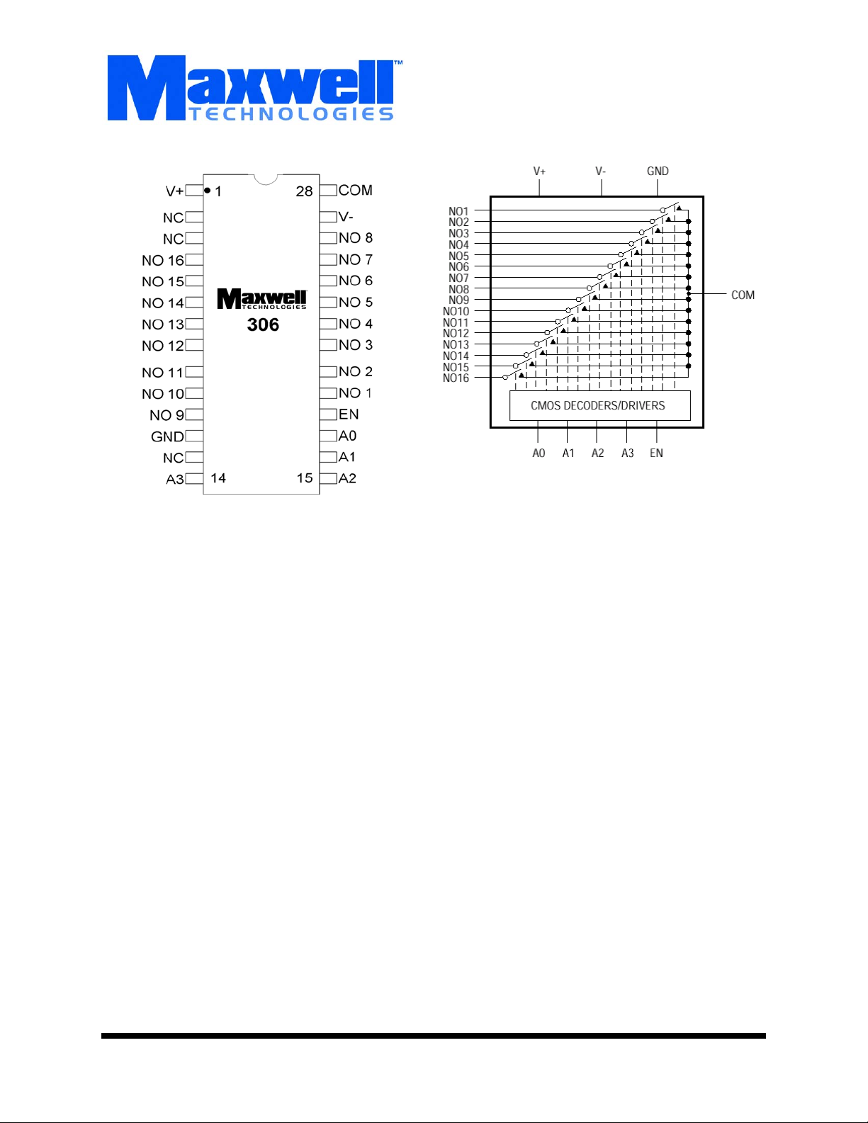
16-Channel CMOS
Analog Multiplexer
Logic Diagram
306
Memory
FEATURES:
•RAD-PAK® technology radiation-hardened against natural
space radiation
• Total dose hardness:
- > 50 Krad (Si), depending upon space mission
• Excellent Single Event Effects:
- SEL
: > 110 MeV/mg/cm
TH
- SEUTH: > 110 MeV/mg/cm
• Package: 28-pin RAD-PAK® flat pack
• Guaranteed on-resistance matching between channels:
< 5
Ω max
• Low on-resistance < 100
• Guaranteed flat on-resistance over specified signal range:
7
Ω max
• Guaranteed Charge Injection: < 10 pC
•I
•I
• ESD Protection > 2000V
• Single-supply operation (+4.5V to +30V)
• Bipolar-supply operation (±4.5V to ±20V)
• Low power consumption, < 1.25 mW
• Rail-to-rail signal handling
• TTL/CMOS-logic compatible
Leakage < 2.5 nA at +85°C
NO(OFF)
COM(OFF)
Leakage < 20 nA at +85°C
2
2
Ω max
Maxwell Technologies’ 306 high-performance, high-precision,
monolithic, CMOS analog multiplexer features a greater than
50 krad (Si) total dose tolerance, depending upon space mission. The patented radiation-hardened R
incorporates radiation shielding in the microcircuit package.
Using Maxwell’s radiation hardened R
nology, this single-ended 1-of-16 device offers very low (less
than 100
between channels and remains flat over the specified analog
signal range. The 306 also offers low leakage over temperature and fast switching speeds. The 306 operates with a single
+4.5V to +30V supply, or bipolar ±4.5V to ± 20V supplies,
while retaining TTL/CMOS- logic input compatibility and fast
switching.
Maxwell Technologies' patented Rad-Pak packaging technology incorporates radiation shielding in the microcircuit package. It eliminates the need for box shielding while providing
the required radiation shielding for a lifetime in orbit or a space
mission.In a GEO orbit, Rad-Pak provides greater than 50
krad (Si) total radiation dose tolerance, dependent upon space
mission. This product is available with packaging and screening up to Class S.
Ω) on-resistance which is matched to within 5Ω
AD-PAK packaging tech-
AD-PAK
®
technology
DESCRIPTION:
1000543
(858) 503-3300 - Fax: (858) 503-3301 - www.maxwell.com
12.20.01 Rev 5
All data sheets are subject to change without notice
©2001 Maxwell Technologies
All rights reserved.
1
Page 2
16-Channel CMOS Analog Multiplexer
TABLE 1. PINOUT DESCRIPTION
PIN SYMBOL DESCRIPTION
1 V+ Positive Supply Voltage Input
2, 3, 13 NC No Internal Connections
4-11 NO16-NO9 Analog Inputs-bidirectional
12 GND Ground
14-17 A3-A0 Address Inputs
18 EN Enable Inputs
19-26 NO1-NO8 Analog Inputs-bidirectional
27 V- Negative Supply Voltage Input
28 COM Output-bidirectional
306
TABLE 2. 306 ABSOLUTE MAXIMUM RATINGS
Parameter Symbol Min Max Units
Voltage Referenced to VV+
GND
Digital Inputs, NO, COM
Continuous Current any terminal)
Peak Current, NO or COM (pulsed at 1ms, 10% duty cycle max) 100 mA
Thermal Impedance
Operating Temperature Range: T
Storage Temperature Range: T
1. Signals on NO, COM, A0, A1, A2, A3, or EN exceeding V+ or V- are clamped by internal diodes. Limit forward current to maximum current ratings.
2. Or 30mA (whichever occurs first)
1
2
Θ
V
CC
JC
A
S
-0.3
-0.3
V- -2 V+ +2 V
-- 3.62 °C/W
-55 +125 °C
-65 +150 °C
44
25
30 mA
V
TABLE 3. DELTA LIMITS
PARAMETER VARIATION
Memory
1000543
I+ ±10% of specified value in table 5
I- ±10% of specified value in table 5
12.20.01 Rev 5
All data sheets are subject to change without notice
2
©2001 Maxwell Technologies
All rights reserved.
Page 3
16-Channel CMOS Analog Multiplexer
TABLE 4. 306 ELECTRICAL CHARACTERISTICS — SINGLE SUPPLY
(V+ = +12V, V- = 0V, GND = 0V, VAH = +2.4V, VAL = +0.8V, TA = -55 TO +125°C, UNLESS OTHERWISE SPECIFIED.)
P
ARAMETER SYMBOL TEST CONDITIONS
SWITCH
Analog Signal Range
On-Resistance R
DYNAMIC
2
Transition Time t
Enable Turn-ON Time t
Enable Turn-OFF Time t
Charge Injection Q CL = 1.0nF
2
V
NO
V
COM
ONINO
V
COM
TRANSVNO1
V
NO8
V
IN
= -1.0mA
= 3V or 10V
= 8V
= 0V
= 2.4V
Figure 9
ON(EN)VINH
V
V
INL
NO1
= 2.4V
= 0V
= 5V
Figure 11
OFF(EN)VINH
V
V
INL
NO1
= 2.4V
= 0V
= 5V
Figure 11
VNO = 0V
VS = 0
W
306
1
MIN
0--12V
= +25°C -- 120 175
T
A
T
= +25°C -- 130 450 nA
A
T
= +25°C -- -- 600 ns
A
T
= +25°C -- -- 300 ns
A
TA = +25°C -- -- 10 pC
TYP
1
1
UNITS
AX
M
Ω
Memory
1. The Algebraic convention where the most negative value is a minimum and the most positive value a maximum is used in this
data sheet.
2. Guaranteed by design.
1000543
12.20.01 Rev 5
All data sheets are subject to change without notice
3
©2001 Maxwell Technologies
All rights reserved.
Page 4
16-Channel CMOS Analog Multiplexer
306
TABLE 5. 306 ELECTRICAL CHARACTERISTICS - DUAL SUPPLIES
(V+ = +15V, V- = -15V, GND = 0V, VAH = +2.4V, VAL = +0.8V, TA = -55 TO +125°C, UNLESS OTHERWISE SPECIFIED.)
P
ARAMETER SYMBOL TEST CONDITIONS MIN TYP MAX UNITS
SWITCH
2, 3
1
2
4
V
V
∆R
R
I
NO(OFF)VCOM
4
I
COM(OFF)VCOM
4
I
COM(ON)VCOM
NO
COM
ONINO
V
ONINO
V
FLATINO
V
V
V
V
V
V
= -1.0 mA
= ±10V
COM
= -1.0 mA
= ±10V
COM
= -1.0 mA
= +5V or 0V
COM
= ±10
= ±10V
NO
= 0V
EN
= ±10
= ±10V
NO
= 0V
EN
= ±10
= ±10V
NO
-15 -- 15 V
= +25°C -- 60 100
T
A
TA = -55 TO +125°C 125
= +25°C -- 1.5 5
T
A
TA = -55 TO +125°C 8
= +25°C -- 1.8 7
T
A
TA = -55 TO +125°C 10
= -55 TO +125°C -5.0 -- 5.0 nA
T
A
= -55 TO +125°C -40 -- 40 nA
T
A
T
= -55 TO +125°C -50 -- 50 nA
A
sequence each switch
on
I
VA = 2.4V or 15V -1.0 -- 1.0 µA
AH
I
AL
TRANS
OPEN
ON(EN)
VEN = 0V or 2.4V,
V
= 0V
A
= VA = 0V or 4.5V TA = +25°C -- 16 30 µA
EN
T
= -55 TO +125° 75
A
V
= 2.4V,
EN
V
= 0V or 2.4
A(ALL)
= 2.4V,
EN
V
= 0V or 2.4V
A
= +25°C 0.075 0.5 mA
T
A
T
= -55 TO +125°C 1
A
= +25°C -1 -- 1 µA
T
A
T
= -55 TO +125°C -10 10
A
Figure 10 TA = +25°C -- 110 300 ns
T
= -55 TO +125°C 400
A
Figure 12 TA = +25°C 10 40 ns
Figure 11 TA = +25°C -- 130 200 ns
T
= -55 TO +125°C 400
A
-1.0 -- 1.0 µA
Analog Signal Range
On-Resistance R
On-Resistance Matching
Between Channels
On-Resistance Flatness
NO-Off Leakage Current
COM-Off Leakage Current
COM-On Leakage Current
INPUT
Input Current with Input Voltage High
Input Current with Input Voltage Low
SUPPLY
Power-Supply Range ±4.5 -- ±20 V
Positive Supply Current I+ V
Negative Supply Current I- V
DYNAMIC
Transition Time t
Break-Before-Make Interval t
Enable Turn-On Time t
Ω
Ω
Ω
Memory
1000543
12.20.01 Rev 5
All data sheets are subject to change without notice
©2001 Maxwell Technologies
All rights reserved.
4
Page 5

16-Channel CMOS Analog Multiplexer
ARAMETER SYMBOL TEST CONDITIONS MIN TYP MAX UNITS
P
306
Enable Turn-Off Time t
Charge Injection
Off Isolation
1
5
OFF(EN)
V
Crosstalk Between Channels V
Logic Input Capacitance C
NO-Off Capacitance C
COM-Off Capacitance C
COM-On Capacitance C
NO(OFF)
COM(OFF)
COM(ON)
Figure 11 TA = +25°C -- 55 150 ns
T
= -55 TO +125°C 300
A
QCL = 1.0 nF,
V
= 0V,
NO
R
= 0Ω,
S
T
= +25°C -- 2 10 pC
A
Figure 13
ISO
VEN = 0V,
R
= 1 kΩ,
L
f = 100 kHz
,
T
= +25°C -- -69 -- dB
A
Figure 14
CT
VEN = 2.4V,
f = 100 kHz
V
= 1V p-p,
GEN
R
= 1 kΩ,
L
,
T
= +25°C -- -92 -- dB
A
Figure 15
f = 1 MHz TA = +25°C -- 8 -- pF
IN
f = 1 MHz
V
= VNO = 0V
EN
= +25°C -- 8 -- pF
T
A
Figure 16
f = 1 MHz
V
= 2.4V
EN
= +25°C -- 130 -- pF
T
A
Figure 16
f = 1 MHz
V
= 0.8V
EN
= +25°C -- 140 -- pF
T
A
Figure 16
Memory
1. Guaranteed by design.
2. Characterized and not 100% tested.
3.
∆RON = RON
(MAX)
- RON
. On-resistance match between channels and flatness are guaranteed only with specified volt-
(MIN)
ages. Flatness is defined as the difference between the maximum and minimum value of on-resistance as measured at the
extremes of the specified analog signal range.
4. Leakage parameters are 100% tested at the maximum rated hot temperature and guaranteed by correlation at +25°C.
5. Off isolation = 20log V
1000543
COM/VNO
, where V
= output and VNO = input to off switch.
COM
12.20.01 Rev 5
All data sheets are subject to change without notice
5
©2001 Maxwell Technologies
All rights reserved.
Page 6

16-Channel CMOS Analog Multiplexer
306
FIGURE 1. ON-RESISTANCE VS. V
(DUAL SUPPLIES)
COM
Memory
IGURE 2. ON-RESISTANCE VS. V
F
AND TEMPERATURE (DUAL SUPPLIES)
COM
1000543
12.20.01 Rev 5
All data sheets are subject to change without notice
©2001 Maxwell Technologies
All rights reserved.
6
Page 7

16-Channel CMOS Analog Multiplexer
306
FIGURE 3. ON-RESISTANCE VS. V
(SINGLE SUPPLY)
COM
Memory
1000543
12.20.01 Rev 5
All data sheets are subject to change without notice
©2001 Maxwell Technologies
All rights reserved.
7
Page 8

16-Channel CMOS Analog Multiplexer
306
FIGURE 4. ON-RESISTANCE VS. V
AND TEMPERATURE (SINGLE SUPPLY)
COM
Memory
IGURE 5. OFF LEAKAGE VS. TEMPERATURE
F
1000543
12.20.01 Rev 5
All data sheets are subject to change without notice
©2001 Maxwell Technologies
All rights reserved.
8
Page 9

16-Channel CMOS Analog Multiplexer
FIGURE 6. ON LEAKAGE VS. TEMPERATURE
306
Memory
FIGURE 7. CHARGE INJECTION VS. V
COM
1000543
12.20.01 Rev 5
All data sheets are subject to change without notice
©2001 Maxwell Technologies
All rights reserved.
9
Page 10

16-Channel CMOS Analog Multiplexer
FIGURE 8. SUPPLY CURRENT VS. TEMPERATURE
306
Memory
FIGURE 9. OVERVOLTAGE PROTECTION USING EXTERNAL BLOCKING DIODES
1000543
12.20.01 Rev 5
All data sheets are subject to change without notice
©2001 Maxwell Technologies
All rights reserved.
10
Page 11

16-Channel CMOS Analog Multiplexer
FIGURE 10. TRANSITION TIME
306
FIGURE 11. ENABLE SWITCHING TIME
FIGURE 12. BREAK-BEFORE-MAKE INTERVAL
Memory
1000543
306RP
12.20.01 Rev 5
All data sheets are subject to change without notice
©2001 Maxwell Technologies
All rights reserved.
11
Page 12

16-Channel CMOS Analog Multiplexer
FIGURE 13. CHARGE INJECTION
306RP
FIGURE 14. OFF ISOLATION
306
Memory
306RP
1000543
12.20.01 Rev 5
All data sheets are subject to change without notice
©2001 Maxwell Technologies
All rights reserved.
12
Page 13

16-Channel CMOS Analog Multiplexer
FIGURE 15. CROSSTALK
306
Memory
FIGURE 16. NO/COM CAPACITANCE
306RP
1000543
12.20.01 Rev 5
All data sheets are subject to change without notice
©2001 Maxwell Technologies
All rights reserved.
13
Page 14

16-Channel CMOS Analog Multiplexer
FIGURE 17. PACKAGE OUTLINE DIAGRAM
PIN #1 INDEX MARK
e
28LDFP
b
E1
E
A
S1
306
D
c
Memory
Q
E2
L
E3
28-PIN RAD-PAK® FLAT PACKAGE
DIMENSIONS
SYMBOL
MIN NOM MAX
A .190 .207 .224
b .015 .017 .022
c .004 .005 .009
D -- .720 .740
E .380 .410 .420
E1 -- -- .440
E2 .180 .250 --
E3 .030 .080 --
e .050 BSC
L .360 .370 .380
Q .062 .073 .081
S1 .000 .027 --
N28
1000543
F28-02
All dimensions in inches
12.20.01 Rev 5
All data sheets are subject to change without notice
©2001 Maxwell Technologies
All rights reserved.
14
Page 15

16-Channel CMOS Analog Multiplexer
Important Notice:
These data sheets are created using the chip manufacturers published specifications. Maxwell Technologies verifies
functionality by testing key parameters either by 100% testing, sample testing or characterization.
The specifications presented within these data sheets represent the latest and most accurate information available to
date. However, these specifications are subject to change without notice and Maxwell Technologies assumes no
responsibility for the use of this information.
Maxwell Technologies’ products are not authorized for use as critical components in life support devices or systems
without express written approval from Maxwell Technologies.
Any claim against Maxwell Technologies must be made within 90 days from the date of shipment from Maxwell Technologies. Maxwell Technologies’ liability shall be limited to replacement of defective parts.
306
Memory
1000543
12.20.01 Rev 5
All data sheets are subject to change without notice
©2001 Maxwell Technologies
All rights reserved.
15
Page 16

16-Channel CMOS Analog Multiplexer
)
Product Ordering Options
Model Number
306
306
RP
F X
Feature
Screening Flow
Package
Option Details
Monolithic
S = Maxwell Class S
B = Maxwell Class B
E = Engineering (testing @ +25°C
I = Industrial (testing @ -55°C,
+25°C, +125°C)
Memory
F = Flat Pack
1000543
Radiation Feature
Base Product
Nomenclature
12.20.01 Rev 5
RP = R
AD-PAK® package
16-Channel CMOS Analog Multiplexer
All data sheets are subject to change without notice
16
©2001 Maxwell Technologies
All rights reserved.
 Loading...