

Page 1
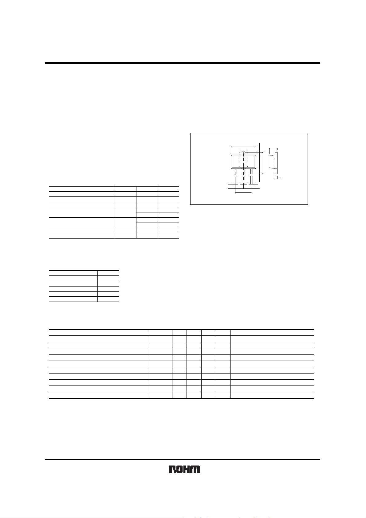
2SD2537
1
2
Transistors
Medium Power Transistor (25V, 1.2A)
2SD2537
zFeatures
1) High DC current gain.
2) High emitter-base voltage. (V
EBO
=12V)
3) Low saturation voltage.
(Max. V
CE(sat)
=0.3V at IC/IB=500mA/10mA)
zAbsolute maximum ratings (Ta=25°C)
Collector-base voltage
Parameter Symbol
Collector-emitter voltage
Emitter-base voltage
Collector current
Collector power dissipation
Junction temperature
Storage temperature
∗1 Single pulse Pw=100ms ∗2 When mounted on a 40×40×0.7mm ceramic board.
V
V
V
P
Tstg
Limits
CBO
CEO
EBO
I
C
C
Tj
30
25
12
1.2
2
0.5 W
2
150
−55 to +150
zPackaging specifications and h
Type
Package
h
FE
Marking
Code
Basic ordering unit (pieces)
2SD2537
MPT3
V
DV
T100
1000
FE
zElectrical characteristics (T a=25°C)
Parameter Symbol Min. Typ. Max. Unit Conditions
Collector-base breakdown voltage
Collector-emitter breakdown voltage
Emitter-base breakdown voltage
Collector cutoff current
Emitter cutoff current
Collector-emitter saturation voltage
Base-emitter saturation voltage
BV
BV
BV
V
V
I
I
CE(sat)
BE(sat)
DC current transfer ratio
Transition frequency
Output capacitance
∗Measured using pulse current.
Cob
A (Pulse)
CBO
CEO
EBO
CBO
EBO
FE
h
f
T
Unit
V
V
V
A (DC)
W
°C
°C
zDimensions (Unit : mm)
2SD2537
ROHM : MPT3
EIAJ : SC-62
∗
∗
30
−
−
25
−
−
12
−
−
200
20
−
−
−
−
0.3
0.3
0.3
1.2 V
1800
−
−
−
−
−
−−
820
−
−
4.5
1.6
(3)(2)(1)
0.5
0.40.4
1.51.5
3.0
C
=10µA
V
I
C
=1mA
I
V
E
=10µA
I
V
V
CB
V
I
C
V
=30V
EB
=12V
/IB=500mA/10mA
µA
µA
IC/IB=0.5A/10mA
V
CE/IC
−
MHz
pF
=5V/0.5A
VCE=10V, IE=−50mA, f=100MHz
CB
=10V, IE=0A, f=1MHz
V
0.5
2.5
1.0
4.0
1.5
0.4
(1) Base
(2) Collector
(3) Emitter
∗
∗
Rev.C 1/3
Page 2
Transistors
)
5
)
s
4
)
0
)
0
)
e
0
0
0
)
e
0
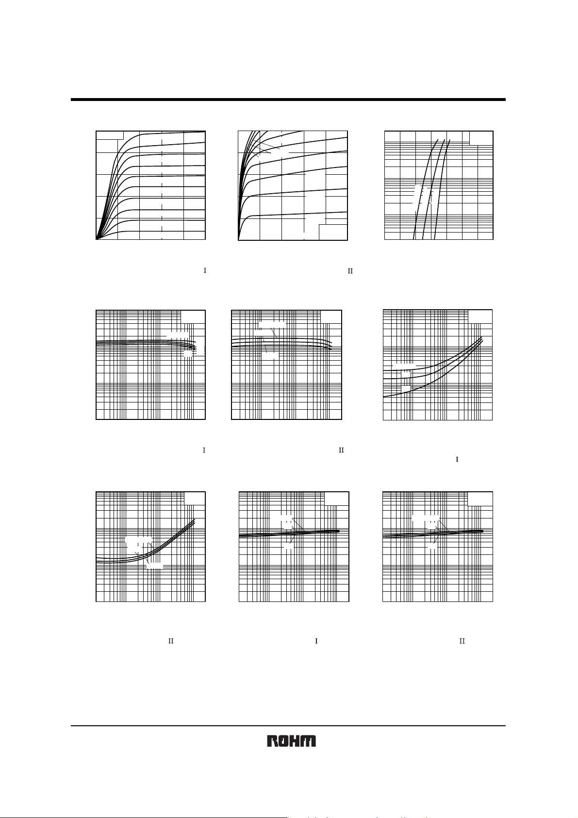
zElectrical characteristics curves
2.0
Ta=25
°C
(mA)
1.6
C
1.2
0.8
0.4
COLLECTOR CURRENT : I
0
0.1 0.2 0.3 0.4 0.
0
COLLECTOR TO EMITTER VOLTAGE : V
Fig.1 Ground emitter output characteristics(
10000
5000
FE
2000
1000
500
200
100
50
DC CURRENT GAIN : h
20
10
2 5 10 20 50
COLLECTOR CURRENT : I
Fig.4 DC current gain vs. collector current (
1000
(mV
500
BE(sat)
200
100
50
20
10
5
Ta=100
°C
25
°C
−25
2.0µA
1.8µA
1.6µA
1.4µA
1.2µA
1.0µA
0.8µA
0.6µA
0.4µA
0.2µA
100 200 500 1000 200
°C
VCE=10V
C
(mA)
IB=0
Ta=25
Pulsed
1V
IC/IB=50
Pulsed
CE
(V)
°C
5V
3V
2.0
(A)
C
1.6
1.2
0.8
0.4
COLLECTOR CURRENT : I
0
3.5mA
3.0mA
2.5mA
4.0mA
4.5mA
5.0mA
0.1 0.2 0.3 0.4 0.50
COLLECTOR TO EMITTER VOLTAGE : VCE (V)
IB=0
2.0mA
1.5mA
1.0mA
0.5mA
Ta=25°C
Pulsed
Fig.2 Ground emitter output characteristics (
10000
5000
FE
2000
1000
500
200
100
50
DC CURRENT GAIN : h
20
10
Ta=100
°C
25
°C
−25
°C
2 5 10 20 50
COLLECTOR CURRENT : I
100 200 500 1000 200
Fig.5 DC current gain vs. collector current (
C
V
Pulsed
(mA)
CE
=5V
10000
5000
(mV)
BE(sat)
2000
1000
500
200
100
IC/IB=10
50
100
50
Ta=25
Pulsed
2000
1000
500
(mA)
C
200
100
50
20
10
5
COLLECTOR CURRENT : I
2
0
BASE TO EMITTER VOLTAGE : V
Fig.3 Ground emitter propagation characteristic
1000
(mV
500
BE(sat)
200
100
50
IC/IB=100
20
50
10
10
5
2
1
COLLECTOR SATURATION VOLTAGE : V
2 5 10 20 50
COLLECTOR CURRENT : I
Fig.6 Collector-emitter saturation voltag
vs. collector current ( )
°C
10000
5000
(mV)
BE(sat)
2000
1000
500
200
100
50
2SD2537
°C
°C
°C
100
−25
25
=
Ta
0.6 0.4 0.2 1.0 0.8 1.2 1.
100 200 500 1000 200
Ta
= −
25
°C
50
100
C
(mA)
V
CE
Pulsed
BE
Ta=25
Pulsed
IC/IB=50
Pulsed
=
5V
(V)
°C
2
1
COLLECTOR SATURATION VOLTAGE : V
2 5 10 20 50
COLLECTOR CURRENT : I
100 200 500 1000 200
C
(mA)
Fig.7 Collector-emitter saturation voltag
vs. collector current ( )
Rev.C 2/3
20
BASE SATURATION VOLTAGE : V
10
2 5 10 20 50
COLLECTOR CURRENT : I
100 200 500 1000 200
C
(mA)
Fig.8 Base-emitter saturation voltage
vs. collector current ( )
20
BASE SATURATION VOLTAGE : V
10
2 5 10 20 50
COLLECTOR CURRENT : I
100 200 500 1000 200
C
(mA)
Fig.9 Base-emitter saturation voltage
vs. collector current ( )
Page 3
Transistors
0
)
)
0
5000
(MHz)
T
2000
1000
500
200
100
50
TRANSITION FREQUENCY : f
20
10
−1 −2 −5 −10 −20 −50 −100 −200 −500 −100
EMITTER CURRENT : I
E
(mA)
CE
=10V
V
Ta=25°C
Pulsed
1000
(pF
500
200
100
50
20
10
5
2
1
COLLECTOR OUTPUT CAPACITANCE : Cob
0.1 0.2 0.5 1 2 5 10 20 50 10
COLLECTOR TO BASE VOLTAGE : V
f=1MHz
I
E
=0A
Ta=25°C
2SD2537
CB
(V
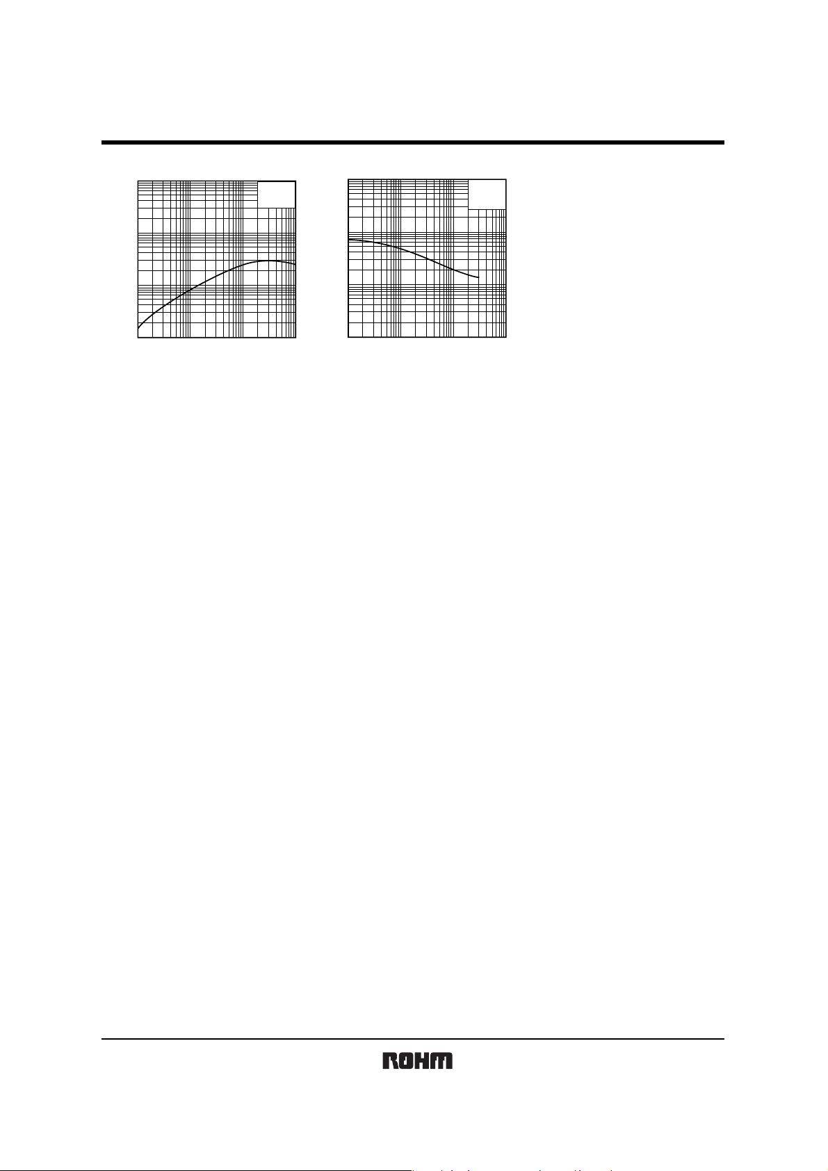
Fig.10 Gain bandwidth product
vs. emitter current
Fig.11 Collector output capacitance
vs. collector-base voltage
Rev.C 3/3
Page 4
Appendix
No technical content pages of this document may be reproduced in any form or transmitted by any
means without prior permission of ROHM CO.,LTD.
The contents described herein are subject to change without notice. The specifications for the
product described in this document are for reference only. Upon actual use, therefore, please request
that specifications to be separately delivered.
Application circuit diagrams and circuit constants contained herein are shown as examples of standard
use and operation. Please pay careful attention to the peripheral conditions when designing circuits
and deciding upon circuit constants in the set.
Any data, including, but not limited to application circuit diagrams information, described herein
are intended only as illustrations of such devices and not as the specifications for such devices. ROHM
CO.,LTD. disclaims any warranty that any use of such devices shall be free from infringement of any
third party's intellectual property rights or other proprietary rights, and further, assumes no liability of
whatsoever nature in the event of any such infringement, or arising from or connected with or related
to the use of such devices.
Upon the sale of any such devices, other than for buyer's right to use such devices itself, resell or
otherwise dispose of the same, no express or implied right or license to practice or commercially
exploit any intellectual property rights or other proprietary rights owned or controlled by
ROHM CO., LTD. is granted to any such buyer.
Products listed in this document are no antiradiation design.
Notes
The products listed in this document are designed to be used with ordinary electronic equipment or devices
(such as audio visual equipment, office-automation equipment, communications devices, electrical
appliances and electronic toys).
Should you intend to use these products with equipment or devices which require an extremely high level of
reliability and the malfunction of with would directly endanger human life (such as medical instruments,
transportation equipment, aerospace machinery, nuclear-reactor controllers, fuel controllers and other
safety devices), please be sure to consult with our sales representative in advance.
About Export Control Order in Japan
Products described herein are the objects of controlled goods in Annex 1 (Item 16) of Export Trade Control
Order in Japan.
In case of export from Japan, please confirm if it applies to "objective" criteria or an "informed" (by MITI clause)
on the basis of "catch all controls for Non-Proliferation of Weapons of Mass Destruction.
Appendix1-Rev1.1
Page 5

 Loading...