

Page 1
SHINDENGEN
Darlington Transistor
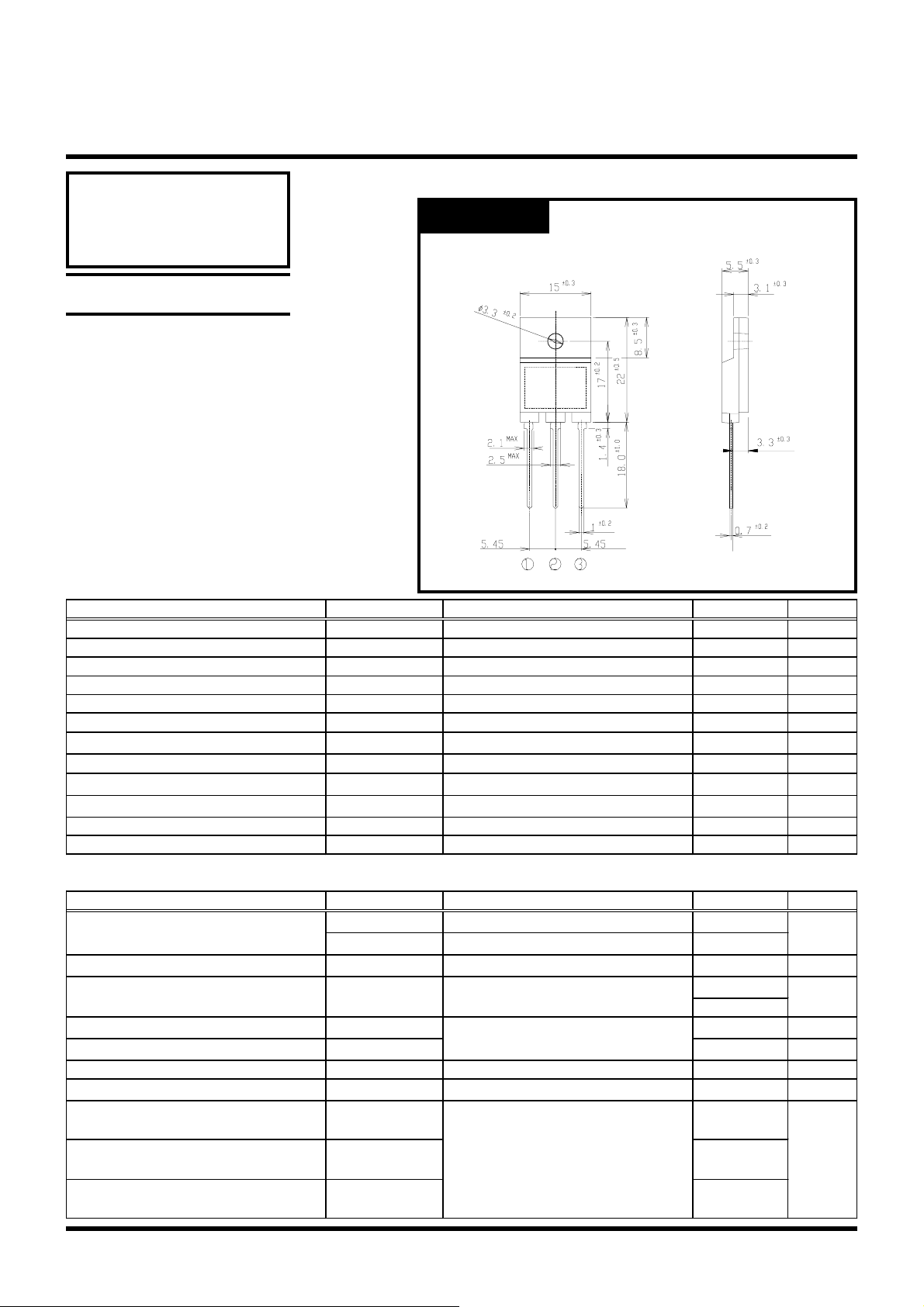
OUTLINE DIMENSIONS
2SD2196
(TP15L20)
15A NPN
RATINGS
●Absolute Maximum Ratings
Item Symbol
Storage Temperature
Junction Temperature
Collector to Base Voltage
Collector to Emitter Voltage
Emitter to Base Voltage
Collector Current DC
Collector Current Peak
Base Current DC
Base Current Peak
Total Transistor Dissipation
Dielectric Strength
Mounting Torque
Case : ITO-3P
Unit : mm
Conditions
Ratings Unit
Tstg -55~+150 ℃
Tj +150 ℃
V
CBO
V
CEO
V
EBO
I
C
I
CP
I
B
I
BP
P
T
Vdis
TOR
Tc = 25℃
Terminals to case AC 1 minute
(Recommended torque : 0.5N・m)
200 V
200 V
7V
15A
22 A
1 A
2A
65 W
2kV
0.8 N・m
●Electrical Characteristics (Tc=25℃)
Item Symbol
Collector Cutoff Current
Emitter Cutoff Current
DC Current Gain
Collector to Emitter Saturation Voltage
Base to Emitter Saturation Voltage
Thermal Resistance
Transition Frequency
Turn on Time
Storage Time
Fall Time
Copyright & Copy;2000 Shindengen Electric Mfg.Co.Ltd
I
CBO
I
CEO
I
EBO
h
FE
VCE(sat)
VBE(sat)
θjc
f
T
ton Max 2
ts
tf
Conditions
VCB = 200V
VCE = 200V
VEB = 7V
V
= 3V, IC = 10A
CE
IC = 10A
IB = 30mA
Junction to case
V
= 10V, IC = 1.5A
CE
IC = 10A
IB1 = IB2 = 30mA
RL = 3Ω
V
= 4V
BB2
Ratings Unit
Max 0.1 mA
Max 0.1
Max 5 mA
Min 1,500
Max 30,000
Max 1.5 V
Max 2.0 V
Max 1.92 ℃/W
TYP 20 MHz
Max 12 μs
Max 5
Page 2
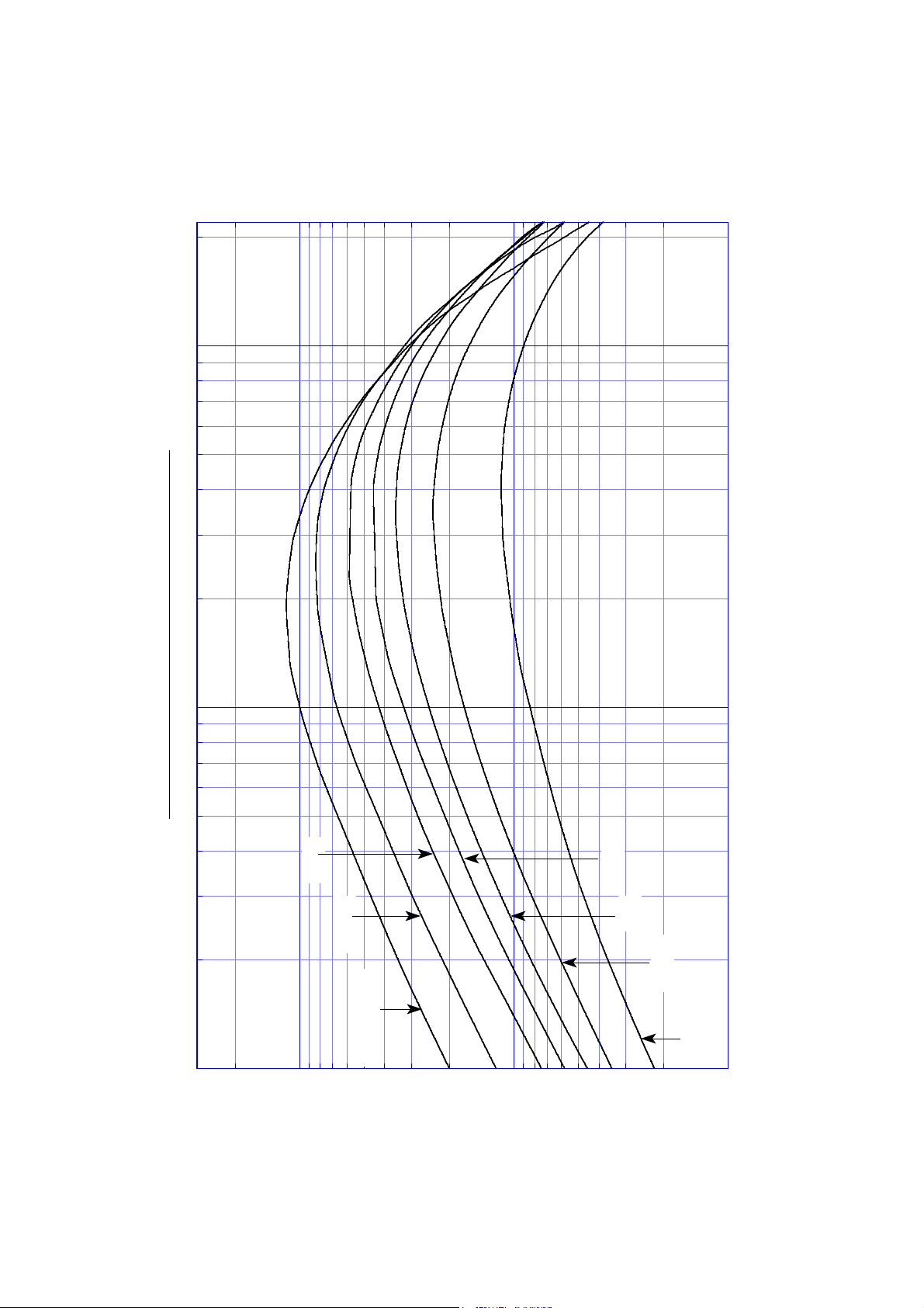
C
- I
FE
h
= 3V
CE
V
22
[A]
C
2SD2196
50°C
100°C
10000
Tc = 150°C
FE
1000
Collector Current I
25°C
0°C
−25°C
−55°C
0.1 1 10
100
DC Current Gain h
Page 3
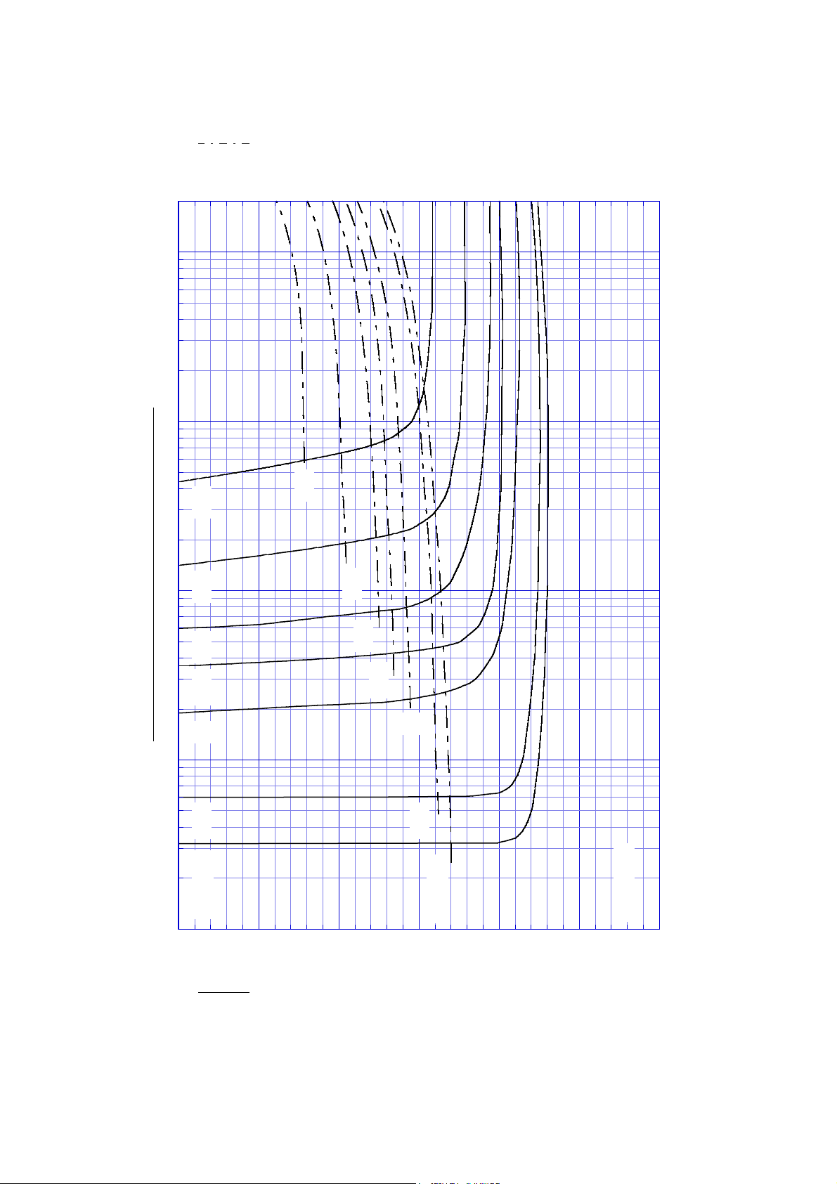
BE
[V]
Base-Emitter Voltage V
3
22A
2.5
Saturation Voltage
22A
2
15A
1.5
1
0.5
0
2000
[mA]
B
2SD2196
= 0.5A 1.5A 5A 7.5A 10A 15A
C
I
3
2.5
CE
[V]
10A
7.5A
5A
1.5A
= 0.5A
C
I
2
1.5
1
0.5
Tc = 25°C
0
0.1 1 10 100 1000
Base Current I
Collector-Emitter Voltage V
Page 4

[µs]
SW
10
2SD2196
Switching Time - I
t
s
t
f
C
1
Switching Time t
0.1
0 5 10 15 20
t
on
Collector Current IC [A]
IB1 = 0.333I
IB2 = 0.333I
V
= 4V
BB2
VCC = 50V
Tc = 25°C
C
C
Page 5

[µs]
SW
10
2SD2196
Switching Time
t
s
t
f
1
Switching Time t
0.1
0 50 100 150 200
t
on
Collector Voltage VCC [V]
IC = 10A
IB1 = 0.033A
IB2 = 0.033A
V
= 4V
BB2
Tc = 25°C
R
= 3Ω
L
Page 6

10
2SD2196
Switching Time - Tc
t
s
[µs]
SW
1
Switching Time t
t
t
f
on
IC = 10A
IB1 = 0.033A
IB2 = 0.033A
V
= 4V
BB2
R
= 5Ω
L
0.1
0 50 100 150
Case Temperature Tc [°C]
Page 7

2
10
1
10
0
10
-1
10
Transient Thermal Impedance
2SD2196
10
1
0.1
0.01
-2
Time t [s]
10
-3
10
-4
10
-5
10
Transient Thermal Impedance θjc(t) [°C/W]
0.001
Page 8

20
10
2SD2196
DC
PT limit
Forward Bias SOA
1ms10ms
150µs
[A]
1
C
Collector Current I
0.1
Tc = 25°C
Single Pulse
I
S/B
limit
0.01
1 10 100
Collector-Emitter Voltage VCE [V]
200
Page 9

2SD2196 Collector Current Derating
100
80
60
40
Collector Current Derating [%]
20
PT limit
I
S/B
limit
VCE = fixed
0
0 50 100 150
Case Temperature Tc [°C]
Page 10

24
20
16
[A]
C
12
2SD2196
Reverse Bias SOA
Collector Current I
8
4
IB1 = 0.002I
IB2 = 0.03A
V
= 5V
BB2
Tc = 25°C
0
0 50 100 150 200
C
Collector-Emitter Voltage VCE [V]
 Loading...