

Page 1
2SD2114K / 2SD2144S
Transistors
High-current Gain Medium
Power T ransistor (20V, 0.5A)
2SD21 14K / 2SD2144S
zFeatures
1) High DC current gain.
h
FE
= 1200 (Typ.)
2) High em i tter-base vol tage.
V
EBO
=12V (Min.)
3) Low V
CE (sat).
VCE
(sat)
= 0.18V (Typ.)
(I
C
/ IB = 500mA / 20mA)
zStructure
Epitaxial planar ty pe
NPN silicon transistor
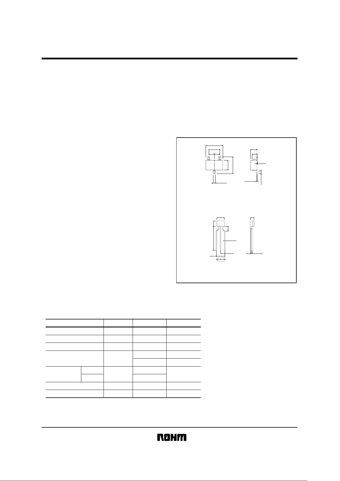
zExternal dimensions (Units : mm)
2SD2144S
2SD2114K
(1) Emitter
(2) Collector
(3) Base
ROHM : SPT
EIAJ : SC-72
0∼0.1
2.8±0.2
1.6
0.3∼0.6
1.1
0.8±0.1
0.15
0.4
2.9±0.2
1.9±0.2
0.95
0.95
+0.2
−0.1
−0.1
+0.2
+0.1
−0.06
+0.1
−0.05
(2)
(1)
(3)
(1) Emitter
(2) Base
(3) Collector
ROHM : SMT3
EIAJ : SC-59
Abbreviated symbol: BB
∗
All terminals have same dimensions
∗
Denotes h
FE
3
±
0.2(15Min.)
4±0.2 2±0.2
0.45
0.5
0.45
5
(1)
(2) (3)
−
0.05
+
0.15
+
0.15
−
0.05
2.5
+
0.4
−
0.1
3Min.
zAbsolute maximum ratings (T a=2 5°C)
Parameter
V
CBO
V
CEO
V
EBO
I
C
P
C
Tj
Tstg
25 V
V
V
A(DC)
W
°C
°C
20
12
0.5
A(Pulse)1
∗
0.2
0.3
150
−55∼+150
Symbol Limits Unit
∗
Single pulse Pw=100ms
2SD2114K
2SD2144S
Collector-base voltage
Collector-emitter voltage
Emitter-base voltage
Collector current
Collector power
dissipation
Junction temperature
Storage temperature
Page 2
2SD2114K / 2SD2144S
Transistors
zElectrical c har acteri stics (Ta=25°C)
Parameter Symbol
BV
CBO
BV
CEO
BV
EBO
I
CBO
I
EBO
V
CE(sat)
f
T
∗
Cob
Min.
25
20
12
−
−
560
−
−
−
−
−
−
−
−
−
0.18
350
8.0
−
−
−
0.5
0.5
2700
0.4
−
−
VI
C
=10µA
I
C
=1mA
I
E
=10µA
V
CB
=20V
V
EB
=10V
I
C/IB
=500mA/20mA
V
CE
=10V, IE=−50mA, f=100MHz
V
CB
=10V, IE=0A, f=1MHz
V
V
µA
µA
−
h
FE
820
2SD2144S
2SD2114K − 2700
V
CE
=3V, IC=10mA
−
V
MHz
pF
Ron − 0.8 − I
B
=1mA, Vi=100mV(rms), f=1kHzpF
Typ. Max. Unit Conditions
Collector-base breakdown voltage
Collector-emitter breakdown voltage
Emitter-base breakdown voltage
Collector cutoff current
Emitter cutoff current
DC current transfer ratio
Collector-emitter saturation voltage
Transition frequency
Output capacitance
Output On-resistance
∗
Measured using pulse current
z
Packaging specifications and h
FE
Package
Code T146 TP
3000 5000
−
−
Taping
Basic ordering
unit (pieces)
VW
h
FE
UVW
2SD2114K
2SD2144S
Type
h
FE
values are classified as follows :
Item U
h
FE
560∼1200V820∼1800W1200∼2700
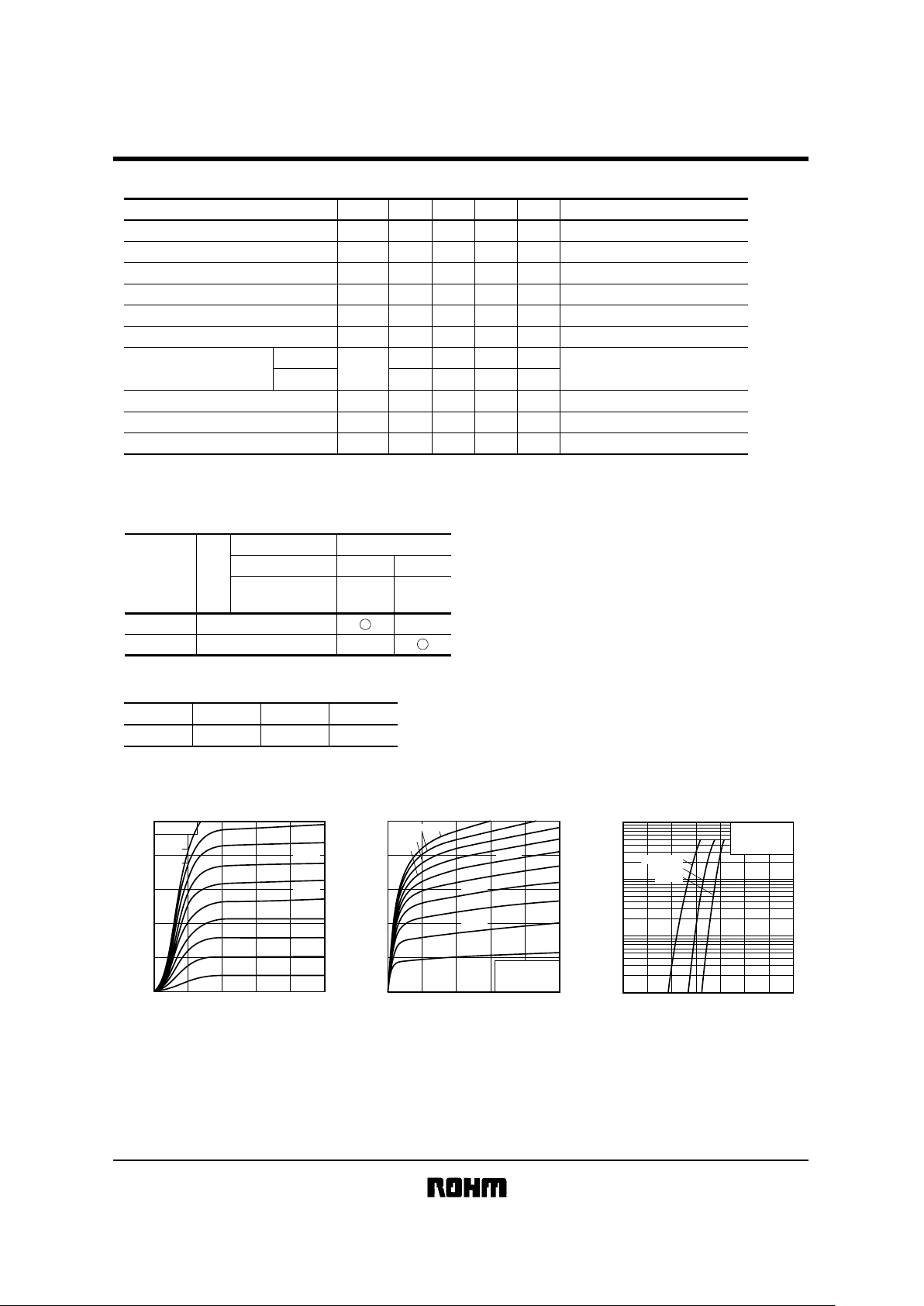
zElectrical c har acteri stic curv es
0
0.4
0.8
1.2
1.6
2.0
0 0.1 0.2 0.3 0.4 0.5
Ta=25˚C
0.2µA
0.4µA
0.6µA
0.8µA
1.0µA
1.2µA
1.4µA
1.6µA
I
B
=0
1.8µA
2.0µA
COLLECTOR CURRENT : I
C
(mA)
COLLECTOR TO EMITTER VOLTAGE : V
CE
(V)
Fig.1 Grounded emitter output
characteristics(Ι)
0
200
400
600
800
1000
0246810
Ta=25°C
Measured using
pulse current.
0.2mA
0.4mA
0.6mA
0.8mA
1.0mA
1.2mA
1.4mA
1.6mA
1.8mA 2.0mA
I
B
=0mA
COLLECTOR CURRENT : I
C
(mA)
COLLECTOR TO EMITTER VOLTAGE : V
CE
(V)
Fig.2 Grounded emitter output
characteristics(ΙΙ)
0 0.2 0.4 0.6 0.8 1.0 1.2 1.4
1
2
5
10
20
50
100
200
500
1000
COLLECTOR CURRENT : I
C
(mA)
BASE TO EMITTER VOLTAGE : V
BE
(V)
Fig.3 Grounded emitter propagation
characteristics
VCE=
3V
Measured using
pulse current.
25°C
−25°C
Ta=100°C
Page 3

2SD2114K / 2SD2144S
Transistors
1 2 5 10 20 50 100 200 5001000
10
20
50
100
200
500
1000
2000
5000
10000
Ta=25°C
Measured using
pulse current.
DC CURRENT GAIN : h
FE
COLLECTOR CURRENT : I
C
(mA)
Fig.4 DC current gain vs. collector
current(Ι)
3V
V
CE
=5V
1V
1 2 5 10 20 50 100 200 500 1000
10000
5000
2000
1000
500
200
100
50
20
10
VCE=
3V
Measured using
pulse current.
DC CURRENT GAIN : h
FE
COLLECTOR CURRENT : I
C
(mA)
Fig.5 DC current gain vs.
collector current(ΙΙ)
25°C
−25°C
Ta=100°C
1
2
2000
1000
200
500
100
20
50
10
5
2 5 10 20 50 100 200 500 1000
Ta=25°C
Measured using
pulse current.
10
25
50
IC/IB=100
COLLECTOR SATURATION VOLTAGE : VCE(sat)
(mV)
COLLECTOR CURRENT : I
C
(mA)
Fig.6 Collector-emitter saturation
voltage vs. collector current(Ι)
COLLECTOR SATURATION VOLTAGE : V
CE(sat)
(mV)
COLLECTOR CURRENT : I
C
(mA)
1
2
2000
1000
200
500
100
20
50
10
5
2 5 10 20 50 100 200 5001000
I
C
/
I
B
=
25
Measured using
pulse current.
Fig.7 Collector-emitter saturation
voltage vs. collector current(ΙΙ)
Ta=100°C
25°C
−25°C
BASE SATURATION VOLTAGE : V
BE(sat)
(mV)
COLLECTOR CURRENT : I
C
(mA)
Fig.8 Base-emitter saturation
voltage vs. collector current(Ι)
1 2 5 10 20 50 100 200 5001000
10000
5000
2000
1000
500
200
100
50
20
10
Ta=25°C
Pulsed
IC/IB=10
25
50
100
1 2 5 10 20 50 100 200 5001000
10000
5000
2000
1000
500
200
100
50
20
10
BASE SATURATION VOLTAGE : V
BE(sat)
(mV)
COLLECTOR CURRENT : I
C
(mA)
Fig.9 Base-emitter saturation voltage
vs. collector current(ΙΙ)
Measured using
pulse current.
l
C/lB
=10
25°C
100°C
Ta=−25°C
EMITTER CURRENT : I
E
(mA)
TRANSITION FREQUENCY : f
T
(MHz)
Fig.10 Gain bandwidth product vs.
emitter current
-1 -2 -5 -10 -20 -50 -100 -200 -500-1000
10000
5000
2000
500
200
1000
100
20
50
10
Ta=25°C
VCE=
10V
Measured using
pulse current.
0.1 0.2 0.5 1 2 5 10 20 50 100
COLLECTOR OUTPUT CAPACITANCE : Cob
(pF)
COLLECTOR TO BASE VOLTAGE : V
CB
(V)
Fig.11 Collector output capacitance
vs. collector-base voltage
100
200
500
1000
10
20
50
2
5
1
Ta=25°C
f
=
1MHz
IE=
0A
0.01 0.020.05 0.1 0.2 0.5 1 2 5 10
ON RESISTANCE : Ron
(Ω)
BASE CURRENT : I
B
(mA)
Fig.12 Output-on resistance vs.
base current
0.1
0.2
0.5
1
2
5
10
20
50
100
Ta=25°C
f=1kHz
Vi=100mV(
rms)
RL=1kΩ
Page 4

2SD2114K / 2SD2144S
Transistors
zRon measurement circuit
Ron= ×R
L
v
0
v
0
vi−v
0
RL=1kΩ
I
B
Output
Input
1kHz
100mV(rms)
v
i
V
 Loading...