

Page 1
DESCURIPTION
A
I
〈Transistor〉
2SC5626
For High Frequency Amplify Application
Silicon NPN Epitaxial Type (Super Mini type)
Mitsubis hi 2SC5626 is a super mini packege resin sealed
silic on NPN epitaxial ty pe t ransistor. It is designed f or high
f requency amplify application.
FEATURE
・Super mini pac kage f or easy mount ing
・High gain band width produc t
PPLICATION
Small t y pe machine high f requency amplif y
applicat ion
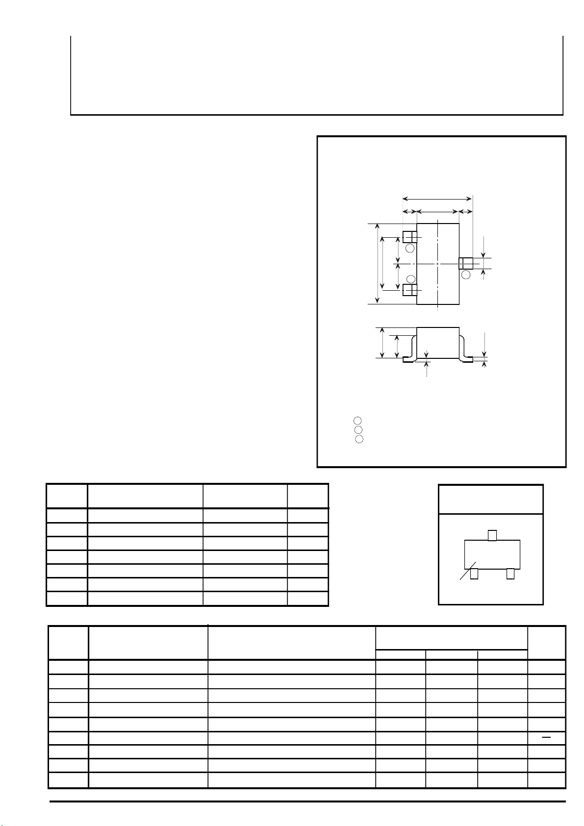
OUTLINE DRAWING
2.1
0.425 0.425
1.25
1.30
1
0.65
2.0
0.65
2
0.9
0.7
0~0.1
TERMINAL CONNECTOR
: BASE
1
: EMITTER
2
: COLLECTOR
3
JEITA : SC-70
JEDEC : -
Unit:mm
0.3
3
0.15
MAXI MUM RATI N GS (Ta=25 ℃)
SYMBOL PARAMETER
VCBO
VEBO
VCEO
I C
PC
Tj
Tstg
SYMBOL
V(BR)CB O
V(BR)CE O I C=100μA, RBE=∞ 20 VC to E break down v oltage
(BR)EB O
V
I CB O
I EBO
hFE
VCE(sat)
f T
Cob
Collector to Base voltage
Emitter to Base voltage
Collector to Emitter voltage
Collec tor current
Col lector diss ipation(Ta= 25℃)
Junction temperature
Storage t emprature
ELECTRICAL CHARACTERISTICS (Ta=25℃)
PARAMETER TEST CONDITION S
C to B break down v oltage
E to B break down v oltage
Collector cut cff current
Emitter cut off current
DC f orward current gain
C to E Saturation voltage
Gain band width product
Col lector output capacitance
RATINGS UNIT
30
4
20
50
150
+150
-55to+150
I C=50μA, I E=0mA
I C=50μA, I C=0m A
VCB=20V, I E=0
EB=3V, I C=0
V
V
CE=10V, I C=5mA
I
C=10mA, I B=1mA
VCE=5V, I E=-10mA
V
CB=6V, I E=0, f =1MH z
V
V
V
mA
mW
℃
℃
MIN
30
4
50
600
TYPE NAME
LIMITS
TY P
148
0.1
1100
1.2
MAR KI N G
S W
MAX
0.5
0.5
0.3
1.5
UNIT
V
V
μA
μA
V
MH z
pF
SAHAYA EL ECTRONICS CORPORATION
Page 2
特性
)
I
〈Transistor〉
2SC5626
For High Frequency Amplify Application
Silicon NPN Epitaxial Type (Super Mini type)
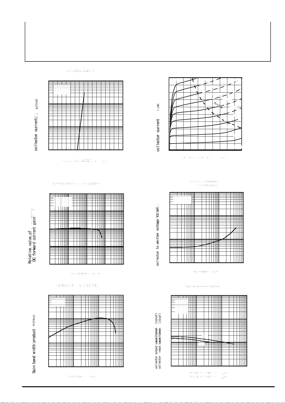
エミッタ接地伝達特性
Common emitter output
100
VCE=6V
Ta=25℃
10
1
0.1
0 0.2 0.4 0.6 0.8 1 1.2 1.4 1.6
base to collector voltage VBE(V)
ベース・エミッタ間電圧 V
DC forward current gain
直流電流増幅率-コレクタ電流特性
VS. collector current
10000
Ta=25℃
VCE=10V
1000
Common emitter transfer
20
180μA
18
16
14
12
10
8
6
4
2
0
0 2 4 6 8 10 12 14 16 18 20
コレクタ・エミッタ間電 圧 VCE(V
(V)
BE
collector to emitter voltage VCE(V)
collector to emitter voltage
VS. collector current
10
Ta=25℃
IC/IB=10/1
1
エミッタ接地出力
160μA
140μA
120μA
コレクタ・エミッタ飽和電圧
-コレクタ電流特性
Ta=25℃
100μA
80μA
60μA
40μA
20μA
IB=0μA
100
10
1
0.1 110 100 1000
collector current IC(mA)
コレクタ電流 I
Gain band width product
利得帯域幅積-エミッタ電流特性
VS. Emitter current
10000
VCE=5V
Ta=25℃
1000
100
10
0.1 1 10100
emitter current IE(mA)
エミッタ電流 I
E (mA)
C(mA)
0.1
0.01
0.11 10 100
collector current IC(mA)
collector output/input capacitance
VS. Collector to Base Voltage
100.0
f=1MHz
IE=0A
IC=0A
Ta=25℃
10.0
1.0
0.1
0.11.010.0 100.0
コレクタ電流 I
入出力容量-ベース電圧特性
Cob
Cib
コレクタ・ベース電圧 V
collector to base voltage VCB(V)
エミッタ・ベース電圧 V
emitter to base voltage VEB(V)
C(mA)
(V)
CB
(V)
EB
SAHAYA EL ECTRONICS CORPORATION
Page 3
I
〈Transistor〉
2SC5626
For High Frequency Amplify Application
Silicon NPN Epitaxial Type (Super Mini type)
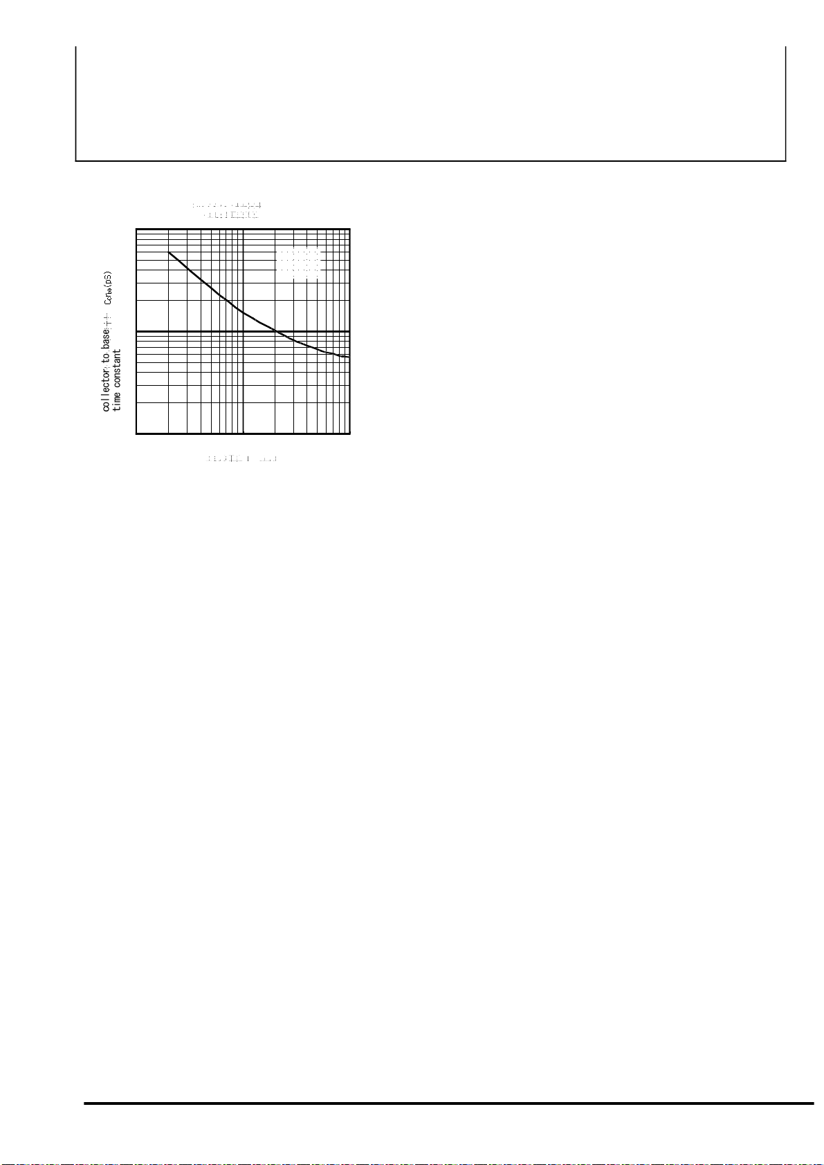
Collector to base time constant
VS. Emitter current
100
10
1
0.1 1.0 10.0
コレクタ・ベース時定数
-エミッタ電流特性
emitter current IE(mA)
エミッタ電流 I
E
(mA)
VCB=5V
f=31.8MHz
Ta=25℃
SAHAYA EL ECTRONICS CORPORATION
Page 4
Keep safety first in your circuit designs!
ion or
the
,
without notice
due to product improvements or other reasons. It is therefore recommended that customers contact ISAHAYA Electronics
before purchasing product listed
ISAHAYA Electronics Corporation products are not designed or manufactured for use in a device or system that is used
e is potentially at stake. Please contact ISAHAYA electronics corporation or an
,
The prior written approval of ISAHAYA Electronics Corporation is necessary to reprint or reproduce in whole or in part these
gies are subject to the Japanese export control restrictions, they must be exported under a
distributor for further details on these
Marketing division, Marketing planning department
6-41 Tsukuba, Isahaya, Nagasaki, 854-0065 Japan
·ISAHAYA Electronics Corporation puts the maximum effort into making semiconductor products better and more reliable, but
there is always the possibility that trouble may occur with them. Trouble with semiconductors may lead to personal injury, fire or
property damage. Remember to give due consideration to safety when making your circuit designs, with appropriate measures
such as (1) placement of substitutive, auxiliary, (2) use of non-farmable material or (3) prevention against any malfunct
mishap.
Notes regarding these materials
·These materials are intended as a reference to our customers in the selection of the ISAHAYA products best suited to
customer’s application; they don't convey any license under any intellectual property rights, or any other rights, belonging
ISAHAYA or third party.
·ISAHAYA Electronics Corporation assumes no responsibility for any damage, or infringement of any third party's rights
originating in the use of any product data, diagrams, charts or circuit application examples contained in these materials.
·All information contained in these materials, including product data, diagrams and charts, represent information on products
at the time of publication of these materials, and are subject to change by ISAHAYA Electronics Corporation
Corporation or an authorized ISAHAYA products distr ibutor for the latest product information
herein.
·
under circumstances in which human lif
authorized ISAHAYA products distributor when considering the use of a product contained herein for any specific purposes
such as apparatus or systems for transportation, vehicular, medical, aerospace, nuclear, or undersea repeater use.
·
materials.
·If these products or technolo
license from the Japanese government and cannot be imported into a country other than the approved destination. Any
diversion or re-export contrary to the export control laws and regulations of Japan and/or the country of destination is
prohibited.
·Please contact ISAHAYA Electronics Corporation or authorized ISAHAYA products
materials or the products contained therein.
Jan.2003
 Loading...