

Page 1
DATA SHEET
SILICON TRANSISTOR
2SC5186
NPN EPITAXIAL SILICON TRANSISTOR IN ULTRA SUPER MINI-MOLD PACKAGE
FOR LOW-NOISE MICROWAVE AMPLIFICATION
FEATURES
• Low Noise
NF = 1.3 dB TYP. @ VCE = 2 V, IC = 3 mA, f = 2 GHz
NF = 1.3 dB
TYP. @ VCE = 1 V, IC = 3 mA, f = 2 GHz
• Ultra Super Mini-Mold package
ORDERING INFORMATION
PART
NUMBER
2SC5186 50 units/box Embossed tape, 8 mm wide,
2SC5186-T1 3 000 units/reel
QUANTITY ARRANGEMENT
Pin 3 (Collector) facing the perforations.
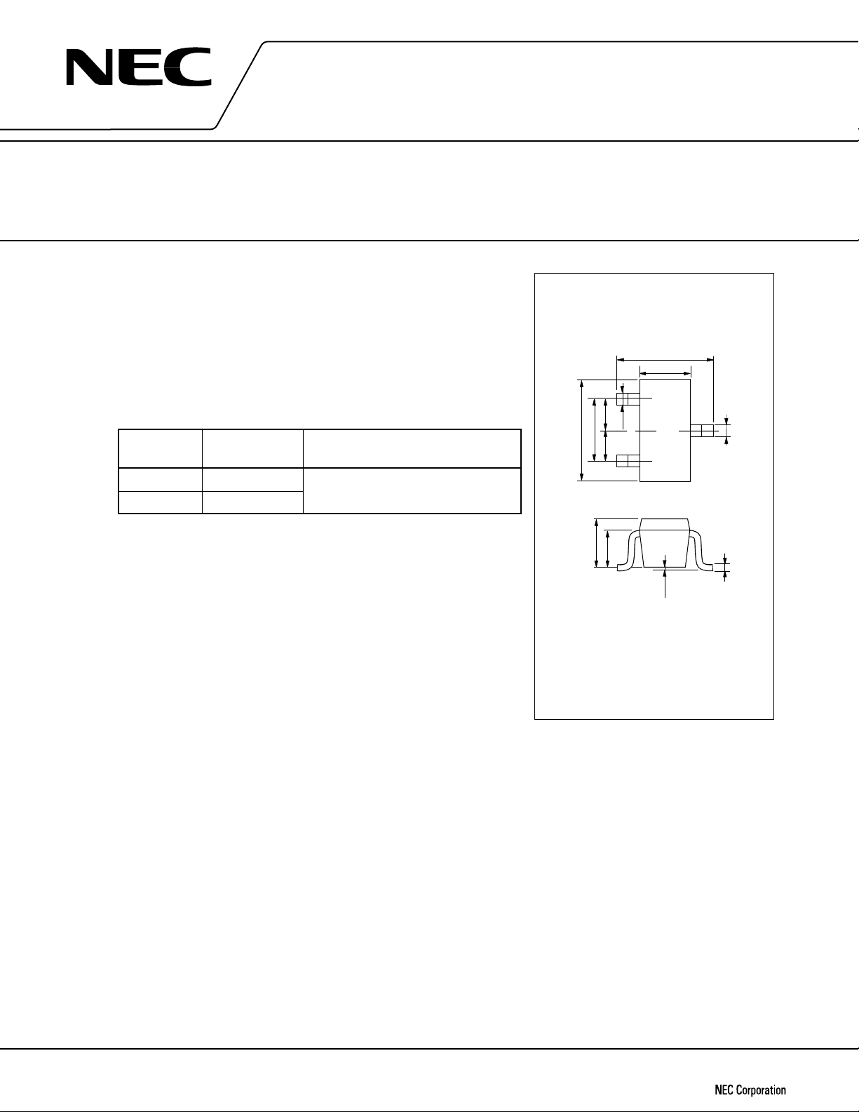
PACKAGE DIMENSIONS
(Units: mm)
1.6 ± 0.1
0.8 ± 0.1
2
+0.1
–0
0.2
86
3
0.5 0.5
1.0
1.6 ± 0.1
1
+0.1
–0
0.3
* Contact your NEC sales representatives to order samples for
evaluation (available in batches of 50).
ABSOLUTE MAXIMUM RATINGS (TA = 25 ˚C)
Collector to Base Voltage VCBO 5V
Collector to Emitter Voltage VCEO 3V
Emitter to Base Voltage VEBO 2V
Collector Current I
Total Power Dissipation PT 90 mW
Junction Temperature Tj 150 ˚ C
Storage Temperature T
C 30 mA
stg –65 to +150 ˚C
0.6
0.75 ± 0.05
PIN CONNECTIONS
1. Emitter
2. Base
3. Collector
0 to 0.1
+0.1
–0.05
0.15
Caution; This transistor uses high-frequency technology. Be careful not to allow excessive current to flow through the transistor, including static electricity.
Document No. P12110EJ2V0DS00 (2nd edition)
(Previous No. TC-2483)
Date Published November 1996 N
Printed in Japan
©
1994
Page 2
ELECTRICAL CHARACTERISTICS (TA = 25 ˚C)
PARAMETER SYMBOL MIN. TYP. MAX. UNIT CONDITIONS
Collector Cutoff Current ICBO 100 nA VCB = 5 V, IE = 0
Emitter Cutoff Current IEBO 100 nA VEB = 1 V, IC = 0
DC Current Gain hFE 70 140 VCE = 2 V, IC = 20 mA
Insertion Power Gain (1) |S21e|
Insertion Power Gain (2) |S21e|
Noise Figure (1) NF 1.3 2.0 dB VCE = 2 V, IC = 3 mA, f = 2 GHz
Noise Figure (2) NF 1.3 2.0 dB VCE = 1 V, IC = 3 mA, f = 2 GHz
Gain Bandwidth Product (1) fT 911 GHzVCE = 2 V, IC = 20 mA, f = 2 GHz
Gain Bandwidth Product (2) fT 79 GHzVCE = 1 V, IC = 10 mA, f = 2 GHz
Feed-back Capacitance Cre 0.4 0.8 pF VCB = 2 V, IE = 0 mA, f = 1 MHz
2
8.5 10 dB VCE = 2 V, IC = 20 mA, f = 2 GHz
2
6.0 7.5 dB VCE = 1 V, IC = 10 mA, f = 2 GHz
*1
*1 Measured with pulses: Pulse width ≤ 350 µs, duty clcye ≤ 2 %, pulsed.
*2 Measured with a three-terminal bridge. The emitter and case terminal are connected to the guard terminal
of the bridge.
2SC5186
*2
FE Class
h
Class FB
Marking 86
hFE 70 to 140
2
Page 3
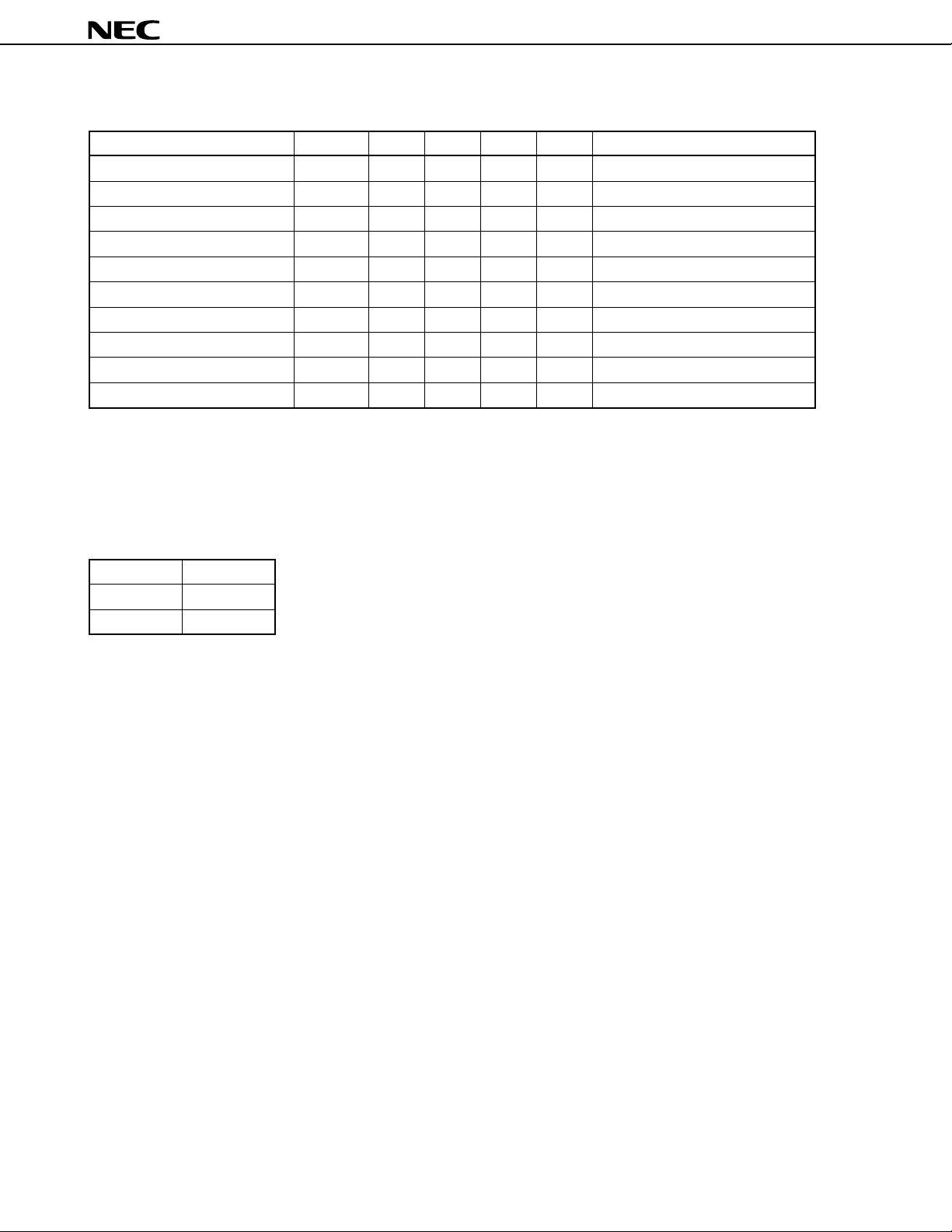
CHARACTERISTICS CURVES (TA = 25 ˚C)
2SC5186
TOTAL POWER DISSIPATION
vs. AMBIENT TEMPERATURE
200
100
90 mW
PT - Total Power Dissipation - mW
0
COLLECTOR CURRENT
vs. COLLECTOR TO EMITTER VOLTAGE
50
T
A - Ambient Temperature - ˚C
25
20
15
10
5
IC - Collector Current - mA
0
1.0 2.0 3.0
V
CE - Collector to Emitter Voltage - V
Passive air cooling
100 150
200 A
µ
180 A
µ
160 A
µ
140 A
µ
120 A
µ
100 A
µ
80 A
µ
60 A
µ
40 A
µ
IB = 20 A
µ
COLLECTOR CURRENT
vs. BASE TO EMITTER VOLTAGE
50
CE = 2 V
V
40
30
20
10
IC - Collector Current - mA
0
BE - Base to Emitter Voltage - V
V
0.5 1.0
DC CURRENT GAIN vs.
COLLECTOR CURRENT
500
200
100
50
VCE = 2 V
VCE = 1 V
hFE - DC Current Gain
20
10
1 2 5 10 20 50 100
IC - Collector Current - mA
GAIN BANDWIDTH PRODUCT
vs. COLLECTOR CURRENT
f = 2 GHz
15
10
5
fT - Gain Bandwidth Product - GHz
1
2 3 5 7 10 20 30
I
C - Collector Current - mA
VCE = 2 V
VCE = 1 V
INSERTION POWER GAIN
vs. COLLECTOR CURRENT
f = 2 GHz
10
5
- Insertion Power Gain - dB
2
|S21e|
0
12357102030
I
C - Collector Current - mA
VCE = 2 V
VCE = 1 V
3
Page 4
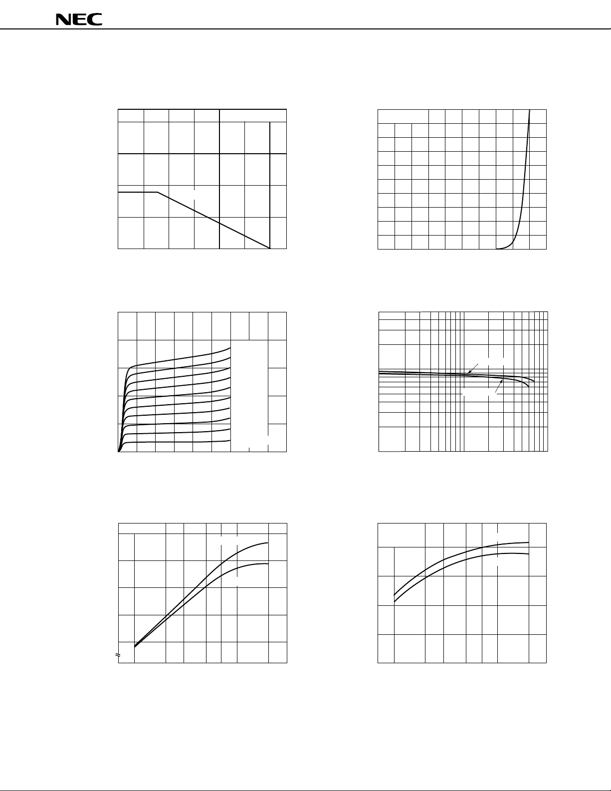
2SC5186
NOISE FIGURE
vs. COLLECTOR CURRENT
3
2
VCE = 1 V
NF - Noise Figure - dB
1
VCE = 2 V
1
I
C
- Collector Current - mA
f = 2 GHz
2
35710 2030
FEED-BACK CAPACITANCE
vs. COLLECTOR TO BASE VOLTAGE
0.8
0.6
0.4
0.2
- Feed-back Capacitance - pF
re
C
0.0
2.0 4.0 6.0 8.0 10.0
CB
- Collector to Base Voltage - V
V
f = 1 MHz
4
Page 5

S-PARAMETERS
VCE = 1 V, IC = 1 mA, ZO = 50 Ω
FREQUENCY S11 S21 S12 S22
2SC5186
MHz
600.00
800.00
1000.00
1200.00
1400.00
1600.00
1800.00
2000.00
2200.00
VCE = 1 V, IC = 3 mA, ZO = 50 Ω
FREQUENCY S11 S21 S12 S22
MHz
600.00
800.00
1000.00
1200.00
1400.00
1600.00
1800.00
2000.00
2200.00
MAG
0.849
0.729
0.661
0.600
0.546
0.503
0.479
0.432
0.408
MAG
0.587
0.475
0.402
0.351
0.319
0.313
0.305
0.297
0.310
ANG
–51.2
–67.5
–83.1
–96.6
–110.6
–125.3
–137.9
–151.1
–166.1
ANG
–77.1
–96.8
–112.4
–127.9
–144.1
–158.2
–169.6
176.3
162.4
MAG
3.157
2.868
2.633
2.501
2.334
2.147
2.038
1.862
1.687
MAG
6.278
5.167
4.424
3.969
3.480
3.106
2.884
2.586
2.313
ANG
134.7
121.5
108.9
99.1
91.2
82.3
74.1
68.4
61.1
ANG
117.3
104.5
93.6
86.1
79.7
72.4
66.8
62.7
56.7
MAG
0.121
0.162
0.189
0.202
0.217
0.231
0.225
0.222
0.218
MAG
0.094
0.120
0.136
0.151
0.164
0.179
0.187
0.195
0.203
ANG
55.5
47.2
40.4
35.1
30.5
27.5
27.3
24.8
21.0
ANG
47.5
44.7
43.1
42.8
41.2
41.7
42.7
42.1
39.5
MAG
0.898
0.797
0.703
0.664
0.617
0.567
0.515
0.481
0.452
MAG
0.675
0.544
0.453
0.409
0.361
0.325
0.289
0.263
0.244
ANG
–29.3
–35.8
–43.2
–50.1
–55.0
–59.2
–63.8
–68.2
–72.9
ANG
–45.1
–51.6
–58.0
–63.0
–66.8
–71.1
–76.7
–80.5
–87.2
VCE = 1 V, IC = 5 mA, ZO = 50 Ω
FREQUENCY S11 S21 S12 S22
MHz
600.00
800.00
1000.00
1200.00
1400.00
1600.00
1800.00
2000.00
2200.00
MAG
0.449
0.362
0.302
0.271
0.257
0.261
0.266
0.272
0.293
ANG
–91.8
–113.0
–128.0
–144.6
–161.3
–173.5
176.1
163.7
151.0
MAG
7.506
5.961
5.003
4.408
3.813
3.389
3.125
2.795
2.492
ANG
109.0
97.4
87.8
81.5
75.6
69.1
64.3
60.7
55.2
MAG
0.081
0.102
0.122
0.138
0.157
0.172
0.186
0.196
0.206
ANG
47.3
50.2
47.4
49.3
48.8
48.1
48.7
48.4
45.3
MAG
0.545
0.428
0.350
0.314
0.272
0.243
0.216
0.196
0.181
ANG
–52.2
–57.6
–63.2
–66.8
–71.0
–75.8
–82.6
–86.9
–95.5
5
Page 6

VCE = 1 V, IC = 7 mA, ZO = 50 Ω
FREQUENCY S11 S21 S12 S22
2SC5186
MHz
600.00
800.00
1000.00
1200.00
1400.00
1600.00
1800.00
2000.00
2200.00
VCE = 1 V, IC = 10 mA, ZO = 50 Ω
FREQUENCY S11 S21 S12 S22
MHz
600.00
800.00
1000.00
1200.00
1400.00
1600.00
1800.00
2000.00
2200.00
MAG
0.363
0.305
0.246
0.233
0.230
0.242
0.248
0.262
0.287
MAG
0.299
0.259
0.216
0.211
0.220
0.234
0.242
0.258
0.286
ANG
–103.5
–125.6
–140.7
–157.3
–174.1
176.0
166.7
154.8
144.5
ANG
–115.1
–136.8
–153.1
–169.2
175.5
167.5
159.6
148.9
139.9
MAG
8.197
6.389
5.312
4.636
3.987
3.540
3.255
2.904
2.584
MAG
8.638
6.657
5.505
4.774
4.093
3.633
3.334
2.967
2.638
ANG
103.6
93.1
84.4
78.7
73.3
67.1
62.8
59.5
54.3
ANG
99.5
90.0
81.9
76.8
71.6
65.7
61.7
58.6
53.6
MAG
0.073
0.093
0.116
0.134
0.154
0.174
0.188
0.199
0.210
MAG
0.063
0.088
0.114
0.135
0.155
0.174
0.191
0.203
0.215
ANG
50.7
51.1
52.8
53.4
53.2
51.5
52.0
51.7
48.4
ANG
55.2
55.8
54.9
56.2
56.1
54.6
54.0
53.7
50.1
MAG
0.457
0.355
0.286
0.253
0.223
0.195
0.174
0.158
0.146
MAG
0.386
0.299
0.239
0.209
0.183
0.162
0.143
0.132
0.124
ANG
–56.6
–61.0
–65.9
–68.6
–73.6
–80.4
–88.2
–92.6
–103.6
ANG
–60.1
–63.7
–67.4
–70.6
–75.3
–83.7
–93.4
–99.4
–112.4
VCE = 1 V, IC = 20 mA, ZO = 50 Ω
FREQUENCY S11 S21 S12 S22
MHz
600.00
800.00
1000.00
1200.00
1400.00
1600.00
1800.00
2000.00
2200.00
MAG
0.232
0.226
0.204
0.210
0.230
0.251
0.256
0.278
0.305
ANG
–144.0
–160.4
–177.5
169.4
159.6
154.6
148.1
139.7
133.0
MAG
8.936
6.790
5.587
4.809
4.105
3.648
3.336
2.965
2.629
ANG
93.2
85.0
77.9
73.5
68.6
63.0
59.5
56.7
51.8
MAG
0.061
0.087
0.112
0.136
0.159
0.179
0.196
0.209
0.222
ANG
59.1
61.6
60.3
61.4
59.2
58.5
57.0
55.9
51.8
MAG
0.267
0.206
0.163
0.142
0.123
0.109
0.100
0.094
0.098
ANG
–67.1
–69.5
–73.6
–77.2
–85.0
–96.4
–110.7
–118.8
–136.9
6
Page 7

VCE = 1 V, IC = 30 mA, ZO = 50 Ω
FREQUENCY S11 S21 S12 S22
2SC5186
MHz
600.00
800.00
1000.00
1200.00
1400.00
1600.00
1800.00
2000.00
2200.00
VCE = 2 V, IC = 1 mA, ZO = 50 Ω
FREQUENCY S11 S21 S12 S22
MHz
600.00
800.00
1000.00
1200.00
1400.00
1600.00
1800.00
2000.00
2200.00
MAG
0.240
0.241
0.228
0.239
0.261
0.280
0.284
0.307
0.334
MAG
0.867
0.751
0.680
0.619
0.560
0.508
0.480
0.435
0.403
ANG
–159.0
–171.1
172.8
161.7
154.0
149.7
144.2
136.9
130.5
ANG
–47.1
–62.5
–77.2
–90.3
–102.9
–116.7
–129.2
–142.2
–157.1
MAG
8.660
6.559
5.394
4.631
3.951
3.513
3.208
2.848
2.522
MAG
3.217
2.947
2.722
2.597
2.449
2.254
2.144
1.980
1.809
ANG
90.9
83.1
76.1
71.9
67.0
61.4
58.0
55.2
50.3
ANG
137.6
124.9
112.8
103.0
95.4
86.8
78.8
73.0
65.6
MAG
0.060
0.085
0.113
0.138
0.159
0.181
0.200
0.210
0.225
MAG
0.103
0.138
0.165
0.180
0.195
0.205
0.204
0.204
0.201
ANG
66.5
63.7
61.7
62.9
61.0
58.8
57.9
56.5
52.1
ANG
55.4
49.1
42.2
38.7
34.2
31.6
31.2
28.7
25.3
MAG
0.224
0.171
0.135
0.116
0.098
0.090
0.087
0.083
0.093
MAG
0.913
0.829
0.740
0.705
0.665
0.618
0.568
0.532
0.505
ANG
–69.0
–72.7
–78.8
–80.5
–91.1
–107.9
–122.8
–132.8
–150.5
ANG
–25.8
–31.4
–38.1
–44.4
–49.0
–52.3
–56.4
–60.8
–65.1
VCE = 2 V, IC = 3 mA, ZO = 50 Ω
FREQUENCY S11 S21 S12 S22
MHz
600.00
800.00
1000.00
1200.00
1400.00
1600.00
1800.00
2000.00
2200.00
MAG
0.611
0.489
0.410
0.346
0.307
0.286
0.273
0.255
0.260
ANG
–69.3
–86.9
–102.1
–115.4
–130.9
–146.1
–158.2
–173.1
172.1
MAG
6.591
5.496
4.728
4.259
3.769
3.365
3.120
2.802
2.511
ANG
120.5
107.8
97.0
89.5
83.3
76.0
70.1
66.1
60.3
MAG
0.081
0.107
0.127
0.136
0.151
0.165
0.173
0.180
0.187
ANG
51.1
46.9
45.4
46.1
45.0
44.8
46.4
45.6
43.4
MAG
0.721
0.595
0.507
0.463
0.419
0.382
0.346
0.321
0.303
ANG
–39.2
–44.7
–49.9
–54.1
–56.7
–59.5
–63.6
–67.3
–72.0
7
Page 8

VCE = 2 V, IC = 5 mA, ZO = 50 Ω
FREQUENCY S11 S21 S12 S22
2SC5186
MHz
600.00
800.00
1000.00
1200.00
1400.00
1600.00
1800.00
2000.00
2200.00
VCE = 2 V, IC = 7 mA, ZO = 50 Ω
FREQUENCY S11 S21 S12 S22
MHz
600.00
800.00
1000.00
1200.00
1400.00
1600.00
1800.00
2000.00
2200.00
MAG
0.465
0.364
0.295
0.250
0.226
0.220
0.214
0.211
0.229
MAG
0.369
0.289
0.224
0.194
0.183
0.185
0.188
0.194
0.215
ANG
–81.0
–99.5
–114.2
–128.7
–146.1
–161.2
–173.2
172.1
158.4
ANG
–90.4
–109.7
–123.7
–139.8
–159.0
–173.1
175.2
161.5
149.9
MAG
8.012
6.426
5.408
4.784
4.169
3.704
3.414
3.049
2.717
MAG
8.842
6.950
5.784
5.068
4.383
3.887
3.574
3.182
2.834
ANG
112.0
100.5
90.8
84.5
78.9
72.3
67.2
63.8
58.5
ANG
106.4
96.0
87.2
81.5
76.4
70.2
65.7
62.4
57.5
MAG
0.068
0.093
0.111
0.127
0.143
0.160
0.170
0.182
0.193
MAG
0.064
0.086
0.105
0.125
0.143
0.159
0.176
0.184
0.196
ANG
50.5
51.8
50.5
52.0
51.9
51.7
51.7
51.7
48.6
ANG
53.1
54.5
53.3
56.1
55.6
55.2
55.3
54.2
51.3
MAG
0.599
0.483
0.403
0.368
0.332
0.302
0.272
0.253
0.239
MAG
0.517
0.412
0.339
0.309
0.280
0.256
0.229
0.213
0.202
ANG
–44.8
–49.0
–53.0
–56.0
–57.9
–60.7
–65.2
–68.5
–74.5
ANG
–47.9
–50.5
–53.7
–56.0
–58.1
–60.9
–65.7
–69.4
–76.2
VCE = 2 V, IC = 10 mA, ZO = 50 Ω
FREQUENCY S11 S21 S12 S22
MHz
600.00
800.00
1000.00
1200.00
1400.00
1600.00
1800.00
2000.00
2200.00
MAG
0.294
0.234
0.180
0.158
0.158
0.168
0.174
0.185
0.208
ANG
–98.0
–119.0
–134.2
–151.6
–170.0
176.2
166.0
153.4
144.0
MAG
9.407
7.292
6.034
5.254
4.520
4.010
3.682
3.271
2.905
ANG
102.2
92.7
84.5
79.5
74.5
68.6
64.4
61.5
56.7
MAG
0.057
0.081
0.104
0.123
0.142
0.161
0.177
0.187
0.200
ANG
55.6
55.5
56.6
59.2
58.9
57.5
57.3
56.7
53.1
MAG
0.445
0.358
0.294
0.268
0.243
0.220
0.200
0.184
0.176
ANG
–49.5
–51.8
–53.7
–55.1
–57.7
–60.5
–66.2
–70.2
–77.7
8
Page 9

VCE = 2 V, IC = 20 mA, ZO = 50 Ω
FREQUENCY S11 S21 S12 S22
2SC5186
MHz
600.00
800.00
1000.00
1200.00
1400.00
1600.00
1800.00
2000.00
2200.00
VCE = 2 V, IC = 30 mA, ZO = 50 Ω
FREQUENCY S11 S21 S12 S22
MHz
600.00
800.00
1000.00
1200.00
1400.00
1600.00
1800.00
2000.00
2200.00
MAG
0.187
0.163
0.127
0.130
0.145
0.163
0.170
0.189
0.211
MAG
0.163
0.157
0.130
0.139
0.157
0.177
0.183
0.202
0.228
ANG
–121.6
–140.5
–161.0
–177.8
166.3
157.9
150.5
141.5
134.5
ANG
–135.8
–154.9
–174.3
170.5
158.6
152.4
145.6
137.6
131.8
MAG
10.000
7.630
6.268
5.419
4.642
4.116
3.771
3.345
2.966
MAG
9.983
7.591
6.228
5.367
4.592
4.074
3.728
3.306
2.932
ANG
95.8
87.7
80.6
76.3
71.7
66.1
62.5
59.8
55.3
ANG
93.5
85.9
79.1
75.0
70.5
65.0
61.6
58.9
54.5
MAG
0.050
0.078
0.100
0.121
0.145
0.164
0.181
0.192
0.205
MAG
0.050
0.075
0.100
0.124
0.144
0.164
0.181
0.192
0.206
ANG
65.0
62.2
61.3
63.1
62.9
61.3
60.4
58.9
55.3
ANG
65.2
63.9
63.1
65.6
63.9
62.1
61.3
59.8
55.9
MAG
0.337
0.276
0.227
0.211
0.192
0.172
0.154
0.144
0.137
MAG
0.306
0.254
0.210
0.196
0.180
0.161
0.146
0.133
0.126
ANG
–50.7
–49.8
–51.8
–52.7
–55.1
–59.9
–66.1
–72.1
–81.8
ANG
–50.2
–49.2
–48.9
–50.0
–52.8
–57.3
–64.2
–70.5
-80.6
9
Page 10

[MEMO]
2SC5186
10
Page 11

[MEMO]
2SC5186
11
Page 12

2SC5186
No part of this document may be copied or reproduced in any form or by any means without the prior written
consent of NEC Corporation. NEC Corporation assumes no responsibility for any errors which may appear in
this document.
NEC Corporation does not assume any liability for infringement of patents, copyrights or other intellectual property
rights of third parties by or arising from use of a device described herein or any other liability arising from use
of such device. No license, either express, implied or otherwise, is granted under any patents, copyrights or other
intellectual property rights of NEC Corporation or others.
While NEC Corporation has been making continuous effort to enhance the reliability of its semiconductor devices,
the possibility of defects cannot be eliminated entirely. To minimize risks of damage or injury to persons or
property arising from a defect in an NEC semiconductor device, customers must incorporate sufficient safety
measures in its design, such as redundancy, fire-containment, and anti-failure features.
NEC devices are classified into the following three quality grades:
"Standard", "Special", and "Specific". The Specific quality grade applies only to devices developed based on a
customer designated "quality assurance program" for a specific application. The recommended applications of
a device depend on its quality grade, as indicated below. Customers must check the quality grade of each device
before using it in a particular application.
Standard: Computers, office equipment, communications equipment, test and measurement equipment,
audio and visual equipment, home electronic appliances, machine tools, personal electronic
equipment and industrial robots
Special: Transportation equipment (automobiles, trains, ships, etc.), traffic control systems, anti-disaster
systems, anti-crime systems, safety equipment and medical equipment (not specifically designed
for life support)
Specific: Aircrafts, aerospace equipment, submersible repeaters, nuclear reactor control systems, life
support systems or medical equipment for life support, etc.
The quality grade of NEC devices is "Standard" unless otherwise specified in NEC's Data Sheets or Data Books.
If customers intend to use NEC devices for applications other than those specified for Standard quality grade,
they should contact an NEC sales representative in advance.
Anti-radioactive design is not implemented in this product.
M4 96.5
2
 Loading...