

Page 1
DATA SHEET
SILICON TRANSISTOR
2SC5184
NPN EPITAXIAL SILICON TRANSISTOR IN SUPER MINI-MOLD
PACKAGE FOR LOW-NOISE MICROWAVE AMPLIFICATION
FEATURES
• Low Noise
• NF = 1.3 dB TYP. @ VCE = 2 V, IC = 3 mA, f = 2 GHz
• NF = 1.3 dB
TYP. @ VCE = 1 V, IC = 3 mA, f = 2 GHz
• Super Mini-Mold package
EIAJ: SC-70
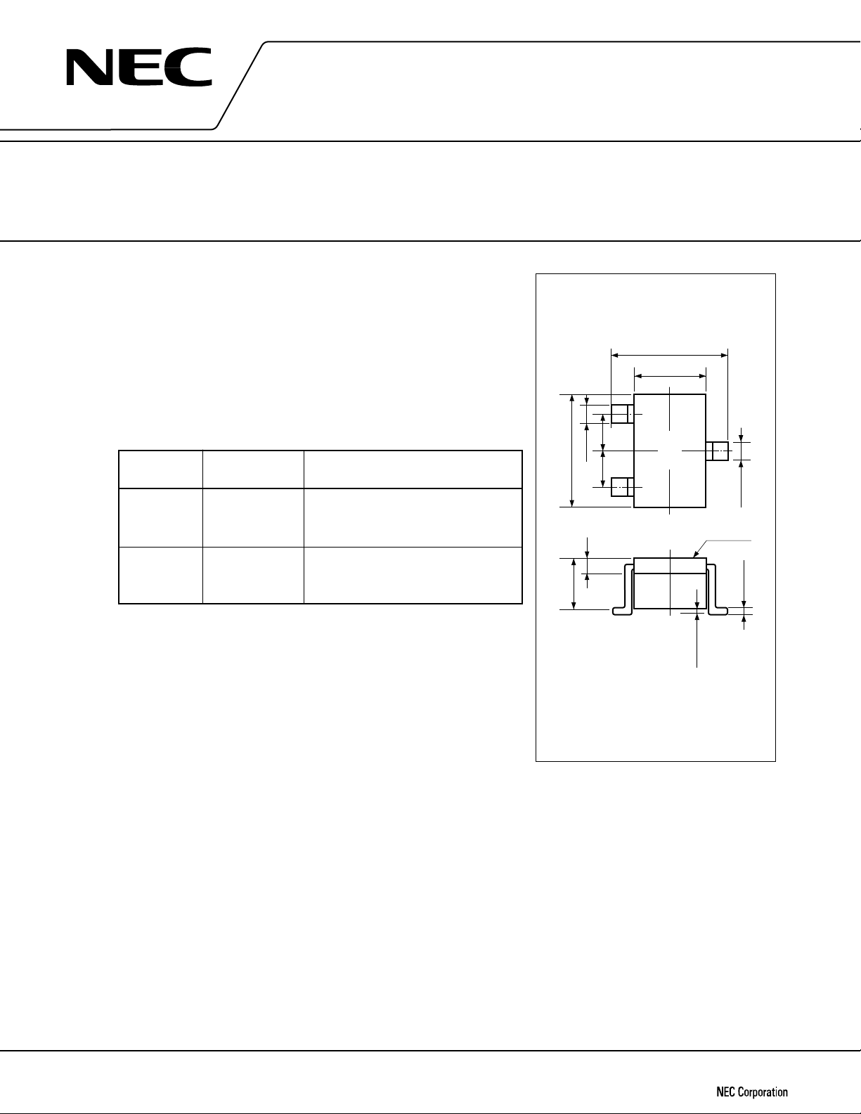
PACKAGE DIMENSIONS
(Units: mm)
2.1 ± 0.1
1.25 ± 0.1
ORDERING INFORMATION
PART
NUMBER
2SC5184-T1 3 000 units/reel Embossed tape, 8 mm wide,
2SC5184-T2 3 000 units/reel Embossed tape, 8 mm wide,
Remark: Contact your NEC sales representative to order samples for
evaluation (available in batches of 50).
QUANTITY ARRANGEMENT
Pin No. 3 (collector)
facing the perforations
Pins No. 1 (emitter) and No. 2 (base)
facing the perforations
ABSOLUTE MAXIMUM RATINGS (TA = 25 ˚C)
Collector to Base Voltage VCBO 5V
Collector to Emitter Voltage VCEO 3V
Emitter to Base Voltage VEBO 2V
Collector Current I
Total Power Dissipation PT 90 mW
Junction Temperature Tj 150 ˚C
Storage Temperature T
C 30 mA
stg –65 to +150 ˚C
+0.1
–0
0.3
2.0 ± 0.2
0.65 0.65
0.3
0.9 ± 0.1
T86
2
1
0 to 0.1
PIN CONNECTIONS
1. Emitter
2. Base
3. Collector
3
+0.1
–0
0.3
Marking
+0.1
–0.05
0.15
Caution; This transistor uses high-frequency technology. Be careful not to allow excessive current to flow through the transistor, including static electricity.
Document No. P12108EJ2V0DS00 (2nd edition)
(Previous No. TC-2481)
Date Published November 1996 N
Printed in Japan
©
1994
Page 2
ELECTRICAL CHARACTERISTICS (TA = 25 ˚C)
PARAMETER SYMBOL MIN. TYP. MAX. UNIT CONDITIONS
Collector Cutoff Current ICBO 100 nA VCB = 5 V, IE = 0
Emitter Cutoff Current IEBO 100 nA VEB = 1 V, IC = 0
DC Current Gain hFE 70 140 VCE = 2 V, IC = 20 mA
Insertion Power Gain (1) |S21e|
Insertion Power Gain (2) |S21e|
Noise Figure (1) NF 1.3 2.0 dB VCE = 2 V, IC = 3 mA, f = 2 GHz
Noise Figure (2) NF 1.3 2.0 dB VCE = 1 V, IC = 3 mA, f = 2 GHz
Gain Bandwidth Product (1) fT 9 11 GHz VCE = 2 V, IC = 20 mA, f = 2 GHz
Gain Bandwidth Product (2) fT 7 9 GHz VCE = 1 V, IC = 10 mA, f = 2 GHz
Feedback Capacitance Cre 0.4 0.8 pF VCB = 2 V, IE = 0 mA, f = 1 MHz
2
2
7 8.5 dB VCE = 2 V, IC = 20 mA, f = 2 GHz
6 7.5 dB VCE = 1 V, IC = 10 mA, f = 2 GHz
*1 Measured with pulses: Pulse width ≤ 350 µs, duty clcye ≤ 2 %, pulsed.
*2 Measured with a three-terminal bridge. The emitter and case terminal are connected to the guard terminal
of the bridge.
*1
2SC5184
*2
FE Class
h
Class FB
Marking T86
hFE 70 to 140
2
Page 3
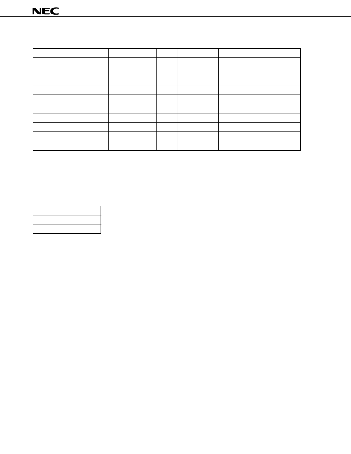
CHARACTERISTICS CURVES (TA = 25 ˚C)
2SC5184
TOTAL POWER DISSIPATION
vs. AMBIENT TEMPERATURE
200
100
- Total Power Dissipation - mW
T
P
90 mW
0 50 100 150
A
- Ambient Temperature - °C
T
COLLECTOR CURRENT vs.
COLLECTOR TO EMITTER VOLTAGE
25
20
200 A
180 A
15
160 A
140 A
120 A
10
- Collector Current - mA
C
I
5
100 A
80 A
µ
60 A
µ
40 A
µ
IB = 20 A
0 1.0 2.0 3.0
VCE - Collector to Emitter Voltage - V
COLLECTOR CURRENT vs.
BASE TO EMITTER VOLTAGE
50
V
CE
= 2 V
40
30
20
- Collector Current - mA
10
C
I
0 0.5 1.0
BE
- Base to Emitter Voltage - V
V
DC CURRENT GAIN vs.
COLLECTOR CURRENT
500
µ
µ
µ
µ
µ
µ
200
100
50
- DC Current Gain
FE
h
VCE = 2 V
VCE = 1 V
20
µ
10
1 2 5 10 20 50 100
IC - Collector Current - mA
GAIN BANDWIDTH PRODUCT
vs. COLLECTOR CURRENT
15
f = 2 GHz
10
5
- Gain Bandwidth Product - dB
T
f
1 2 3 5 7 10
IC - Collector Current - mA
VCE = 2 V
VCE = 1 V
INSERTION POWER GAIN vs.
COLLECTOR CURRENT
10
f = 2 GHz
5
- Insertion Power Gain - dB
2
|
21e
|S
0
1 2 3 5 7 10
IC - Collector Current - mA
VCE = 2 V
VCE = 1 V
3
Page 4
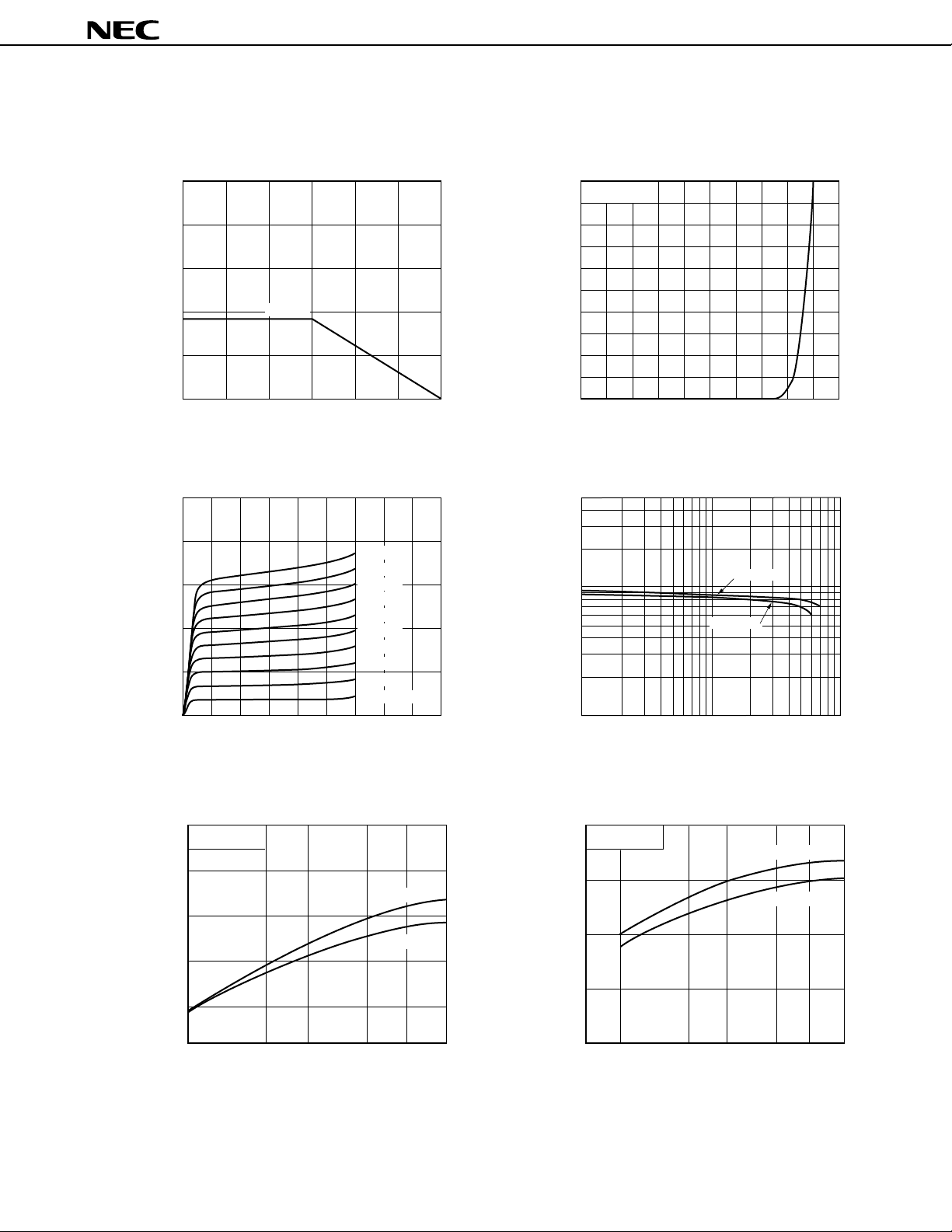
2SC5184
NOISE FIGURE vs.
COLLECTOR CURRENT
3
2
VCE = 2 V
VCE = 1 V
NF - Noise Figure - dB
1
1235710
I
C
- Collector Current - mA
f = 2 GHz
FEED-BACK CAPACITANCE vs.
COLLECTOR TO BASE VOLTAGE
0.8
f = 1 MHz
0.6
0.4
0.2
- Feedback Capacitance - pF
re
C
0 2.0 4.0 6.0 8.0 10.0
V
CB
- Collector to Base Voltage - V
4
Page 5

S-PARAMETERS
VCE = 1 V, IC = 1 mA, ZO = 50 Ω
FREQUENCY S11 S21 S12 S22
2SC5184
MHz
100.0000
200.0000
300.0000
400.0000
500.0000
600.0000
700.0000
800.0000
900.0000
1000.0000
1100.0000
1200.0000
1300.0000
1400.0000
1500.0000
1600.0000
1700.0000
1800.0000
1900.0000
2000.0000
VCE = 1 V, IC = 3 mA, ZO = 50 Ω
MAG
0.974
0.971
0.956
0.926
0.902
0.861
0.829
0.793
0.753
0.723
0.691
0.652
0.628
0.587
0.565
0.535
0.508
0.489
0.471
0.449
ANG
–6.9
–14.0
–20.5
–28.4
–34.5
–42.2
–49.5
–55.6
–63.1
–68.8
–76.3
–82.9
–88.7
–95.8
–101.4
–107.4
–113.5
–118.6
–124.6
–130.5
MAG
2.031
1.953
1.928
2.021
1.911
1.941
1.930
1.864
1.917
1.839
1.838
1.833
1.742
1.756
1.686
1.654
1.624
1.565
1.530
1.509
ANG
170.7
162.5
154.8
147.6
141.1
135.2
129.2
123.6
118.6
114.1
109.3
104.4
100.1
95.7
92.0
88.1
84.7
81.2
78.4
75.2
MAG
0.029
0.057
0.083
0.105
0.126
0.144
0.158
0.172
0.182
0.191
0.200
0.204
0.209
0.213
0.215
0.217
0.218
0.220
0.221
0.222
ANG
84.1
78.0
72.3
67.5
62.9
58.6
54.4
51.1
48.2
45.7
43.4
41.6
39.4
38.4
37.0
36.0
35.3
35.0
34.5
34.6
MAG
0.993
0.982
0.960
0.925
0.902
0.861
0.826
0.791
0.758
0.731
0.703
0.675
0.652
0.629
0.610
0.591
0.574
0.559
0.545
0.532
ANG
–5.5
–10.9
–15.5
–20.7
–24.9
–28.6
–32.6
–35.6
–38.5
–41.3
–43.4
–45.6
–47.9
–49.5
–51.6
–53.0
–54.6
–56.0
–57.4
–59.0
FREQUENCY S11 S21 S12 S22
MHz
100.0000
200.0000
300.0000
400.0000
500.0000
600.0000
700.0000
800.0000
900.0000
1000.0000
1100.0000
1200.0000
1300.0000
1400.0000
1500.0000
1600.0000
1700.0000
1800.0000
1900.0000
2000.0000
MAG
0.917
0.879
0.830
0.755
0.703
0.625
0.560
0.506
0.456
0.411
0.384
0.346
0.327
0.303
0.289
0.273
0.261
0.252
0.247
0.242
ANG
–11.2
–22.2
–31.8
–44.2
–52.5
–63.5
–73.9
–81.8
–90.8
–98.6
–105.7
–113.0
–119.7
–126.4
–132.4
–138.2
–144.4
–150.1
–156.0
–161.8
MAG
5.682
5.447
5.165
5.205
4.838
4.684
4.522
4.219
4.031
3.796
3.574
3.377
3.166
3.011
2.850
2.707
2.588
2.468
2.364
2.274
ANG
164.5
154.3
144.7
136.0
129.3
122.1
115.3
109.8
104.7
100.0
95.9
91.7
88.4
85.2
82.4
79.6
77.1
74.4
72.2
69.8
MAG
0.027
0.052
0.072
0.087
0.101
0.111
0.121
0.129
0.137
0.143
0.152
0.158
0.165
0.171
0.179
0.185
0.193
0.200
0.207
0.214
ANG
81.0
72.7
66.6
61.7
58.1
55.8
54.2
53.3
52.9
52.3
51.9
51.7
51.6
51.8
51.9
51.9
51.9
52.1
52.4
52.4
MAG
0.966
0.914
0.845
0.764
0.705
0.639
0.587
0.543
0.508
0.478
0.451
0.428
0.408
0.390
0.375
0.361
0.348
0.338
0.329
0.319
ANG
–10.7
–20.4
–28.1
–34.6
–39.7
–43.1
–46.8
–49.0
–51.3
–52.9
–54.4
–55.6
–57.2
–58.2
–59.6
–60.2
–61.3
–62.4
–63.4
–64.8
5
Page 6

VCE = 1 V, IC = 7 mA, ZO = 50 Ω
FREQUENCY S11 S21 S12 S22
2SC5184
MHz
100.0000
200.0000
300.0000
400.0000
500.0000
600.0000
700.0000
800.0000
900.0000
1000.0000
1100.0000
1200.0000
1300.0000
1400.0000
1500.0000
1600.0000
1700.0000
1800.0000
1900.0000
2000.0000
VCE = 1 V, IC = 10 mA, ZO = 50 Ω
MAG
0.784
0.700
0.606
0.490
0.412
0.343
0.299
0.265
0.243
0.222
0.213
0.198
0.193
0.184
0.183
0.178
0.177
0.176
0.180
0.182
ANG
–18.0
–36.7
–51.4
–68.6
–80.3
–92.6
–103.1
–111.9
–120.0
–127.7
–135.2
–142.5
–149.8
–156.2
–162.3
–168.3
–173.9
–179.6
175.3
170.6
MAG
11.844
10.881
9.746
9.052
8.022
7.101
6.348
5.687
5.170
4.735
4.360
4.033
3.756
3.508
3.310
3.127
2.963
2.814
2.686
2.573
ANG
157.9
143.4
131.7
121.0
113.0
106.5
101.0
96.8
93.2
89.7
86.9
83.9
81.5
79.0
76.8
74.6
72.7
70.6
68.6
66.9
MAG
0.026
0.045
0.060
0.070
0.081
0.091
0.100
0.110
0.119
0.130
0.140
0.150
0.159
0.169
0.179
0.189
0.199
0.208
0.217
0.228
ANG
77.0
68.8
64.3
62.4
61.4
61.2
62.0
62.1
62.3
62.2
62.3
62.7
62.2
61.9
61.8
61.4
61.0
60.9
60.3
60.0
MAG
0.906
0.784
0.664
0.563
0.496
0.436
0.393
0.359
0.336
0.317
0.298
0.283
0.268
0.257
0.248
0.239
0.231
0.224
0.218
0.211
ANG
–18.0
–32.0
–40.8
–46.7
–50.2
–52.6
–54.8
–55.8
–57.4
–58.1
–59.3
–59.8
–61.4
–62.2
–63.3
–63.8
–65.1
–66.2
–67.3
–68.8
FREQUENCY S11 S21 S12 S22
MHz
100.0000
200.0000
300.0000
400.0000
500.0000
600.0000
700.0000
800.0000
900.0000
1000.0000
1100.0000
1200.0000
1300.0000
1400.0000
1500.0000
1600.0000
1700.0000
1800.0000
1900.0000
2000.0000
MAG
0.689
0.583
0.476
0.372
0.306
0.259
0.232
0.211
0.198
0.184
0.180
0.172
0.172
0.169
0.169
0.168
0.168
0.170
0.175
0.179
ANG
–24.5
–47.9
–65.2
–82.3
–94.2
–106.7
–117.0
–126.3
–134.5
–142.3
–149.3
–156.7
–163.4
–169.2
–175.2
179.9
174.6
169.3
165.1
161.1
MAG
14.893
13.678
11.837
10.296
8.800
7.604
6.695
5.965
5.386
4.901
4.500
4.155
3.851
3.602
3.400
3.189
3.032
2.880
2.748
2.629
ANG
153.4
137.1
124.5
114.1
106.9
101.4
96.9
93.1
90.1
87.1
84.5
82.0
79.5
77.3
75.4
73.1
71.4
69.4
67.6
66.0
MAG
0.024
0.041
0.054
0.065
0.076
0.087
0.098
0.108
0.118
0.128
0.140
0.151
0.161
0.170
0.183
0.193
0.203
0.213
0.224
0.234
ANG
76.0
68.5
65.2
63.8
65.2
65.2
65.5
65.5
65.6
66.0
65.8
65.5
65.1
64.6
64.2
63.8
63.2
62.6
62.0
61.4
MAG
0.865
0.710
0.579
0.483
0.421
0.367
0.331
0.301
0.282
0.265
0.251
0.239
0.226
0.218
0.210
0.203
0.195
0.188
0.184
0.179
ANG
–22.1
–37.1
–45.5
–50.8
–53.5
–55.4
–57.2
–58.0
–59.2
–59.5
–60.8
–61.5
–63.1
–63.8
–65.4
–66.0
–67.1
–68.3
–69.4
–71.4
6
Page 7

VCE = 1 V, IC = 20 mA, ZO = 50 Ω
FREQUENCY S11 S21 S12 S22
2SC5184
MHz
100.0000
200.0000
300.0000
400.0000
500.0000
600.0000
700.0000
800.0000
900.0000
1000.0000
1100.0000
1200.0000
1300.0000
1400.0000
1500.0000
1600.0000
1700.0000
1800.0000
1900.0000
2000.0000
VCE = 2 V, IC = 1 mA, ZO = 50 Ω
MAG
0.441
0.358
0.290
0.242
0.208
0.196
0.190
0.185
0.184
0.182
0.183
0.183
0.187
0.187
0.193
0.193
0.196
0.199
0.205
0.211
ANG
–76.4
–97.6
–111.1
–120.8
–129.8
–142.5
–150.3
–158.8
–164.7
–171.1
–176.2
178.4
173.6
169.5
165.5
161.7
158.0
153.9
151.4
148.9
MAG
18.515
15.403
12.655
10.657
9.000
7.688
6.712
5.955
5.338
4.863
4.468
4.106
3.806
3.540
3.337
3.154
2.980
2.843
2.699
2.579
ANG
138.3
121.3
110.9
104.2
99.0
94.9
91.3
88.1
85.6
82.9
80.7
78.5
76.3
74.3
72.1
70.4
68.7
67.0
65.2
63.6
MAG
0.021
0.037
0.049
0.061
0.073
0.084
0.096
0.108
0.120
0.132
0.144
0.156
0.168
0.179
0.190
0.202
0.214
0.224
0.235
0.247
ANG
73.8
69.2
69.0
69.6
70.4
70.5
70.5
70.5
69.9
69.7
69.3
68.5
68.2
67.5
66.9
65.8
65.3
64.3
63.7
62.9
MAG
0.753
0.556
0.429
0.349
0.301
0.259
0.234
0.212
0.200
0.189
0.179
0.169
0.160
0.154
0.149
0.144
0.138
0.134
0.130
0.127
ANG
–30.4
–46.5
–53.6
–58.2
–59.6
–61.2
–62.7
–63.2
–64.9
–65.0
–67.1
–68.2
–69.9
–71.5
–73.3
–74.4
–76.3
–78.3
–79.8
–82.4
FREQUENCY S11 S21 S12 S22
MHz
100.0000
200.0000
300.0000
400.0000
500.0000
600.0000
700.0000
800.0000
900.0000
1000.0000
1100.0000
1200.0000
1300.0000
1400.0000
1500.0000
1600.0000
1700.0000
1800.0000
1900.0000
2000.0000
MAG
0.978
0.975
0.964
0.932
0.915
0.876
0.846
0.812
0.776
0.746
0.717
0.676
0.652
0.610
0.586
0.554
0.526
0.503
0.482
0.457
ANG
–6.8
–13.1
–19.1
–26.5
–32.1
–39.3
–46.0
–51.8
–58.9
–64.1
–71.2
–77.5
–83.0
–89.8
–95.2
–101.0
–106.7
–111.9
–117.8
–123.4
MAG
2.018
1.958
1.937
2.026
1.917
1.959
1.945
1.888
1.940
1.862
1.875
1.874
1.785
1.802
1.731
1.709
1.681
1.624
1.594
1.572
ANG
171.8
163.5
156.3
149.7
143.3
137.6
132.0
126.6
121.9
117.6
112.8
108.0
103.9
99.6
96.0
92.0
88.6
85.1
82.1
79.0
MAG
0.025
0.049
0.071
0.091
0.110
0.127
0.140
0.152
0.162
0.170
0.177
0.184
0.189
0.192
0.195
0.197
0.198
0.200
0.201
0.202
ANG
83.3
78.9
74.1
68.8
64.8
60.6
57.0
53.7
50.9
48.7
46.4
44.3
42.2
41.0
39.6
39.0
38.3
37.8
37.5
37.6
MAG
0.995
0.987
0.970
0.938
0.920
0.884
0.852
0.822
0.791
0.766
0.740
0.714
0.693
0.669
0.653
0.634
0.616
0.602
0.591
0.575
ANG
–4.9
–9.7
–13.9
–18.4
–22.1
–25.5
–29.1
–31.8
–34.6
–37.1
–39.1
–41.1
–43.1
–44.7
–46.7
–47.8
–49.4
–50.7
–52.0
–53.3
7
Page 8

VCE = 2 V, IC = 3 mA, ZO = 50 Ω
FREQUENCY S11 S21 S12 S22
2SC5184
MHz
100.0000
200.0000
300.0000
400.0000
500.0000
600.0000
700.0000
800.0000
900.0000
1000.0000
1100.0000
1200.0000
1300.0000
1400.0000
1500.0000
1600.0000
1700.0000
1800.0000
1900.0000
2000.0000
VCE = 2 V, IC = 5 mA, ZO = 50 Ω
MAG
0.916
0.893
0.850
0.777
0.731
0.656
0.592
0.536
0.481
0.435
0.400
0.357
0.333
0.302
0.284
0.264
0.247
0.233
0.225
0.215
ANG
–10.2
–20.0
–28.6
–39.7
–47.1
–57.0
–66.2
–73.3
–81.4
–88.0
–95.1
–101.3
–107.4
–113.4
–119.4
–124.8
–130.7
–136.2
–142.5
–148.4
MAG
5.805
5.495
5.238
5.292
4.938
4.818
4.673
4.389
4.223
3.993
3.781
3.589
3.374
3.210
3.047
2.896
2.766
2.641
2.528
2.436
ANG
166.0
155.8
146.7
138.5
131.9
125.0
118.4
113.0
107.8
103.3
99.0
94.9
91.5
88.0
85.2
82.3
79.9
77.2
75.0
72.9
MAG
0.023
0.045
0.062
0.077
0.090
0.101
0.109
0.117
0.123
0.131
0.137
0.144
0.151
0.157
0.164
0.170
0.177
0.183
0.191
0.198
ANG
82.8
74.6
68.0
64.1
60.3
58.5
56.7
55.5
55.0
54.5
54.5
54.2
54.0
54.1
54.4
54.4
54.7
54.7
55.1
54.9
MAG
0.973
0.931
0.870
0.798
0.745
0.684
0.633
0.591
0.557
0.528
0.504
0.479
0.459
0.441
0.427
0.414
0.401
0.392
0.383
0.373
ANG
–9.3
–17.8
–24.4
–30.4
–34.8
–37.8
–41.0
–42.9
–44.8
–46.2
–47.6
–48.5
–49.8
–50.5
–51.7
–52.3
–53.2
–54.0
–54.8
–55.8
FREQUENCY S11 S21 S12 S22
MHz
100.0000
200.0000
300.0000
400.0000
500.0000
600.0000
700.0000
800.0000
900.0000
1000.0000
1100.0000
1200.0000
1300.0000
1400.0000
1500.0000
1600.0000
1700.0000
1800.0000
1900.0000
2000.0000
MAG
0.857
0.811
0.743
0.642
0.571
0.483
0.415
0.363
0.321
0.284
0.260
0.231
0.215
0.196
0.185
0.172
0.163
0.155
0.152
0.149
ANG
–13.2
–25.8
–36.6
–50.1
–59.3
–69.9
–79.3
–86.7
–93.7
–100.3
–106.6
–112.8
–119.2
–125.0
–131.8
–137.4
–144.2
–150.5
–157.2
–164.1
MAG
9.113
8.527
7.907
7.737
7.109
6.609
6.140
5.613
5.182
4.803
4.448
4.149
3.875
3.635
3.428
3.244
3.090
2.938
2.810
2.692
ANG
162.6
150.3
139.9
130.5
123.0
115.5
109.1
104.2
99.9
95.9
92.6
89.2
86.4
83.8
81.3
78.9
76.6
74.6
72.6
70.7
MAG
0.023
0.041
0.057
0.069
0.079
0.088
0.096
0.105
0.113
0.121
0.130
0.137
0.146
0.155
0.163
0.171
0.180
0.188
0.196
0.205
ANG
78.8
72.1
66.2
63.9
61.7
61.2
60.5
60.2
60.2
60.5
60.6
60.4
60.7
60.7
60.7
60.7
60.5
60.3
60.3
60.0
MAG
0.948
0.870
0.781
0.690
0.627
0.564
0.517
0.479
0.451
0.427
0.406
0.388
0.372
0.359
0.348
0.337
0.327
0.319
0.313
0.305
ANG
–12.7
–23.3
–30.9
–36.6
–40.3
–42.6
–44.8
–45.9
–47.4
–47.9
–48.9
–49.5
–50.4
–51.0
–52.1
–52.3
–53.0
–53.7
–54.5
–55.4
8
Page 9

VCE = 2 V, IC = 10 mA, ZO = 50 Ω
FREQUENCY S11 S21 S12 S22
2SC5184
MHz
100.0000
200.0000
300.0000
400.0000
500.0000
600.0000
700.0000
800.0000
900.0000
1000.0000
1100.0000
1200.0000
1300.0000
1400.0000
1500.0000
1600.0000
1700.0000
1800.0000
1900.0000
2000.0000
VCE = 2 V, IC = 20 mA, ZO = 50 Ω
MAG
0.805
0.733
0.645
0.531
0.445
0.366
0.311
0.269
0.240
0.212
0.194
0.174
0.161
0.148
0.141
0.132
0.127
0.122
0.123
0.123
ANG
–16.8
–31.1
–43.8
–58.4
–68.3
–78.6
–87.2
–94.4
–101.0
–107.4
–113.9
–120.4
–127.7
–134.2
–141.3
–147.6
–154.8
–161.7
–169.0
–175.7
MAG
12.051
11.136
10.084
9.504
8.484
7.598
6.839
6.153
5.628
5.139
4.750
4.399
4.097
3.836
3.613
3.403
3.231
3.069
2.919
2.802
ANG
160.5
145.9
134.6
124.1
116.3
109.4
103.8
99.5
95.7
92.4
89.4
86.5
84.0
81.6
79.2
77.2
75.1
73.1
71.1
69.5
MAG
0.021
0.039
0.052
0.063
0.073
0.083
0.092
0.100
0.110
0.119
0.128
0.137
0.146
0.155
0.164
0.174
0.182
0.192
0.201
0.210
ANG
76.4
71.1
66.7
64.9
64.6
64.2
63.5
63.8
63.6
64.0
63.9
64.1
63.5
64.4
64.2
63.5
63.3
63.0
62.6
62.2
MAG
0.923
0.818
0.711
0.615
0.550
0.492
0.451
0.416
0.393
0.374
0.355
0.341
0.326
0.316
0.307
0.298
0.290
0.283
0.277
0.271
ANG
–15.4
–27.3
–34.9
–39.8
–42.8
–44.5
–46.1
–46.7
–47.7
–48.1
–48.9
–49.3
–50.1
–50.6
–51.6
–51.8
–52.4
–53.1
–54.1
–55.0
FREQUENCY S11 S21 S12 S22
MHz
100.0000
200.0000
300.0000
400.0000
500.0000
600.0000
700.0000
800.0000
900.0000
1000.0000
1100.0000
1200.0000
1300.0000
1400.0000
1500.0000
1600.0000
1700.0000
1800.0000
1900.0000
2000.0000
MAG
0.723
0.629
0.520
0.403
0.327
0.266
0.228
0.196
0.175
0.155
0.143
0.129
0.121
0.114
0.109
0.105
0.102
0.101
0.105
0.108
ANG
–20.3
–38.3
–53.2
–67.5
–76.9
–86.7
–95.0
–102.2
–109.0
–116.2
–123.2
–130.1
–138.7
–145.5
–153.5
–160.3
–168.2
–176.1
177.1
171.3
MAG
15.896
14.304
12.506
11.061
9.540
8.285
7.319
6.522
5.905
5.381
4.958
4.574
4.251
3.961
3.732
3.520
3.341
3.172
3.013
2.886
ANG
156.6
140.5
128.1
117.4
110.0
104.2
99.5
95.8
92.5
89.5
86.8
84.3
81.9
79.8
77.7
75.7
74.0
72.0
70.3
68.6
MAG
0.021
0.036
0.048
0.059
0.069
0.079
0.088
0.098
0.107
0.117
0.128
0.137
0.147
0.157
0.166
0.176
0.186
0.196
0.205
0.215
ANG
78.2
71.0
67.3
67.5
66.7
67.1
67.3
67.3
67.2
67.0
67.2
67.2
66.8
66.7
66.5
65.7
65.3
64.8
64.3
64.0
MAG
0.890
0.755
0.633
0.541
0.480
0.427
0.393
0.363
0.343
0.329
0.313
0.301
0.289
0.281
0.273
0.266
0.259
0.253
0.248
0.242
ANG
–18.6
–31.2
–38.5
–42.4
–44.5
–45.6
–46.6
–46.7
–47.5
–47.6
–48.2
–48.6
–49.3
–49.7
–50.7
–51.0
–51.7
–52.8
–53.5
–54.2
9
Page 10

VCE = 2 V, IC = 20 mA, ZO = 50 Ω
FREQUENCY S11 S21 S12 S22
2SC5184
MHz
100.0000
200.0000
300.0000
400.0000
500.0000
600.0000
700.0000
800.0000
900.0000
1000.0000
1100.0000
1200.0000
1300.0000
1400.0000
1500.0000
1600.0000
1700.0000
1800.0000
1900.0000
2000.0000
MAG
0.474
0.354
0.270
0.213
0.173
0.146
0.129
0.116
0.104
0.097
0.093
0.091
0.090
0.089
0.091
0.094
0.095
0.100
0.106
0.106
ANG
–33.9
–57.5
–73.3
–85.2
–94.8
–105.1
–115.0
–124.7
–133.8
–143.0
–151.3
–159.0
–169.5
–176.4
177.3
170.6
165.4
160.1
156.6
150.5
MAG
27.070
20.499
15.719
12.575
10.387
8.873
7.714
6.794
6.117
5.522
5.083
4.649
4.346
4.044
3.797
3.565
3.378
3.222
3.080
2.922
ANG
147.2
127.1
115.1
107.5
101.9
97.6
93.9
91.0
88.4
85.2
83.4
81.0
79.0
77.1
75.6
73.8
71.8
70.2
68.4
67.1
MAG
0.018
0.031
0.043
0.054
0.064
0.074
0.084
0.095
0.106
0.116
0.128
0.137
0.148
0.159
0.169
0.179
0.190
0.200
0.210
0.219
ANG
76.5
74.3
72.8
71.2
72.6
73.1
72.7
72.0
72.5
72.4
71.7
71.1
70.9
70.5
69.5
68.9
68.2
67.6
66.9
66.3
MAG
0.805
0.624
0.501
0.424
0.376
0.337
0.312
0.294
0.279
0.266
0.257
0.250
0.241
0.234
0.229
0.224
0.218
0.216
0.210
0.204
ANG
–24.1
–36.4
–42.1
–44.2
–44.6
–44.9
–45.2
–44.9
–45.8
–44.9
–45.7
–46.1
–46.9
–47.2
–48.7
–49.5
–50.2
–50.7
–52.1
–52.9
10
Page 11

[MEMO]
2SC5184
11
Page 12

2SC5184
No part of this document may be copied or reproduced in any form or by any means without the prior written
consent of NEC Corporation. NEC Corporation assumes no responsibility for any errors which may appear in
this document.
NEC Corporation does not assume any liability for infringement of patents, copyrights or other intellectual property
rights of third parties by or arising from use of a device described herein or any other liability arising from use
of such device. No license, either express, implied or otherwise, is granted under any patents, copyrights or other
intellectual property rights of NEC Corporation or others.
While NEC Corporation has been making continuous effort to enhance the reliability of its semiconductor devices,
the possibility of defects cannot be eliminated entirely. To minimize risks of damage or injury to persons or
property arising from a defect in an NEC semiconductor device, customers must incorporate sufficient safety
measures in its design, such as redundancy, fire-containment, and anti-failure features.
NEC devices are classified into the following three quality grades:
"Standard", "Special", and "Specific". The Specific quality grade applies only to devices developed based on a
customer designated "quality assurance program" for a specific application. The recommended applications of
a device depend on its quality grade, as indicated below. Customers must check the quality grade of each device
before using it in a particular application.
Standard: Computers, office equipment, communications equipment, test and measurement equipment,
audio and visual equipment, home electronic appliances, machine tools, personal electronic
equipment and industrial robots
Special: Transportation equipment (automobiles, trains, ships, etc.), traffic control systems, anti-disaster
systems, anti-crime systems, safety equipment and medical equipment (not specifically designed
for life support)
Specific: Aircrafts, aerospace equipment, submersible repeaters, nuclear reactor control systems, life
support systems or medical equipment for life support, etc.
The quality grade of NEC devices is "Standard" unless otherwise specified in NEC's Data Sheets or Data Books.
If customers intend to use NEC devices for applications other than those specified for Standard quality grade,
they should contact an NEC sales representative in advance.
Anti-radioactive design is not implemented in this product.
M4 96.5
2
 Loading...