

Page 1
Transistor
2SC4543
Silicon NPN epitaxial planer type
For video amplifier
Features
■
●
High transition frequency fT.
●
Small collector output capacitance Cob.
●
Wide current range.
Absolute Maximum Ratings (Ta=25˚C)
■
Parameter
Collector to base voltage
Collector to emitter voltage
Collector to emitter voltage
Emitter to base voltage
Peak collector current
Collector current
Collector power dissipation
Junction temperature
Storage temperature
*1
REB = 1.2kΩ
*2
Printed circuit board: Copper foil area of 1cm2 or more, and the board
thickness of 1.7mm for the collector portion
Symbol
V
CBO
V
CER
V
CEO
V
EBO
I
CP
I
C
*2
P
C
T
j
T
stg
*1
Ratings
110
100
50
3.5
300
150
1.0
150
–55 ~ +150
Unit
V
V
V
V
mA
mA
W
˚C
˚C
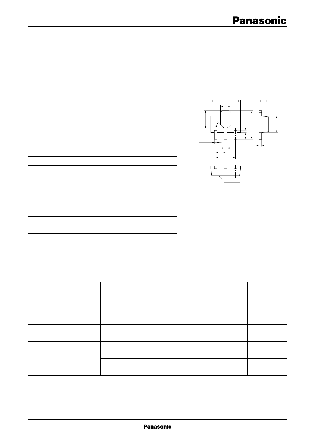
4.5±0.1
1.6±0.2
2.6±0.1
45°
0.4±0.08
0.5±0.08
1.5±0.1
3.0±0.15
321
marking
1:Base
2:Collector EIAJ:SC–62
3:Emitter Mini Power Type Package
1.5±0.1
–0.20
+0.25
0.4max.1.0
4.0
–0.2
+0.1
Marking symbol : 1F
Unit: mm
2.5±0.1
0.4±0.04
Electrical Characteristics (Ta=25˚C)
■
Parameter
Collector cutoff current
Collector to base voltage
Collector to emitter voltage
Emitter to base voltage
Forward current transfer ratio
Collector to emitter saturation voltage
Transition frequency
Collector output capacitance
Symbol
I
CEO
V
CBO
V
CER
V
CEO
V
EBO
h
FE
V
CE(sat)
f
T1
f
T2
C
ob
Conditions
VCE = 35V, IB = 0
IC = 100µA, IE = 0
IC = 500µA, RBE = 470Ω
IC = 1mA, IB = 0
IE = 100µA, IC = 0
VCE = 5V, IC = 100mA
IC = 150mA, IB = 15mA
*
*
VCB = 10V, IE = –10mA, f = 200MHz
VCB = 10V, IE = –110mA*, f = 200MHz
VCB = 30V, IE = 0, f = 1MHz
min
110
100
50
3.5
20
typ
max
10
0.5
300
350
3
*
Pulse measurement
Unit
µA
V
V
V
V
V
MHz
MHz
pF
1
Page 2
Transistor 2SC4543
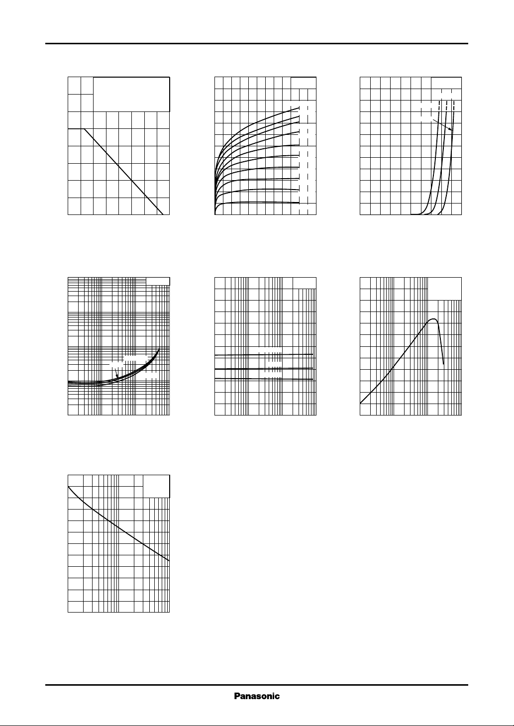
PC — Ta IC — V
1.6
)
1.4
W
(
C
1.2
1.0
0.8
0.6
0.4
0.2
Collector power dissipation P
0
)
100
V
(
30
CE(sat)
10
3
1
0.3
0.1
0.03
0.01
Collector to emitter saturation voltage V
Printed circut board: Copper
foil area of 1cm
the board thickness of 1.7mm
for the collector portion.
0 16040 12080 14020 10060
2
or more, and
Ambient temperature Ta (˚C
V
— I
CE(sat)
1 10 100 10003 30 300
25˚C
C
IC/IB=10
Ta=75˚C
–25˚C
Collector current IC (mA
)
)
CE
240
200
)
mA
(
160
C
120
80
Collector current I
40
0
012108264
IB=5.0mA
Collector to emitter voltage VCE (V
hFE — I
C
120
FE
100
80
60
40
20
Forward current transfer ratio h
0
0.1 1 10 1000.3 3 30
Ta=75˚C
25˚C
–25˚C
Collector current IC (mA
Ta=25˚C
4.5mA
4.0mA
3.5mA
3.0mA
2.5mA
2.0mA
1.5mA
1.0mA
0.5mA
VCE=5V
)
120
100
)
mA
(
80
C
60
40
Collector current I
20
0
01.00.80.2 0.60.4
)
Base to emitter voltage VBE (V
600
)
500
MHz
(
T
400
300
200
100
Transition frequency f
0
–1 –10 –100 –1000–3 –30 –300
IC — V
BE
VCE=5V
Ta=75˚C
–25˚C
fT — I
E
VCB=10V
Ta=25˚C
Emitter current IE (mA
25˚C
)
)
)
pF
(
Cob — V
6
5
ob
4
3
2
1
CB
Collector output capacitance C
0
1 3 10 30 100
Collector to base voltage VCB (V
2
IE=0
f=1MHz
Ta=25˚C
)
 Loading...