

Page 1
Application
VHF / UHF wide band amplifier
Outline
UPAK
3
2SC4422
Silicon NPN Epitaxial
1
2
4
1. Base
2. Collector
3. Emitter
4. Collector (Flange)
Page 2
2SC4422
Absolute Maximum Ratings (Ta = 25°C)
Item Symbol Ratings Unit
Collector to base voltage V
Collector to emitter voltage V
Emitter to base voltage V
Collector current I
Collector power dissipation P
CBO
CEO
EBO
C
C
Junction temperature Tj 150 °C
Storage temperature Tstg –55 to +150 °C
Electrical Characteristics (Ta = 25°C)
Item Symbol Min Typ Max Unit Test conditions
Collector to base breakdown
V
(BR)CBO
voltage
Collector cutoff current I
Emitter cutoff current I
DC current transfer ratio h
CBO
I
CEO
EBO
FE
Collector output capacitance Cob — 1.2 1.6 pF VCB = 5 V, IE = 0, f = 1 MHz
Gain bandwidth product f
T
Power gain PG 7.0 9.0 — dB VCE = 5 V, IC = 20 mA,
Noise figure NF — 1.6 3.0 dB VCE = 5 V, IC = 5 mA,
Note: Marking is “CR”.
15——V I
——1 µAVCB = 12 V, IE = 0
——1 µAVCE = 10 V, RBE = ∞
——1 µAVEB = 1 V, IC = 0
50 — 250 VCE = 5 V, IC = 20 mA
4.5 6.0 — GHz VCE = 5 V, IC = 20 mA
15 V
11 V
2V
50 mA
400 mW
= 10 µA, IE = 0
C
f = 900 MHz
f = 900 MHz
2
Page 3
2SC4422
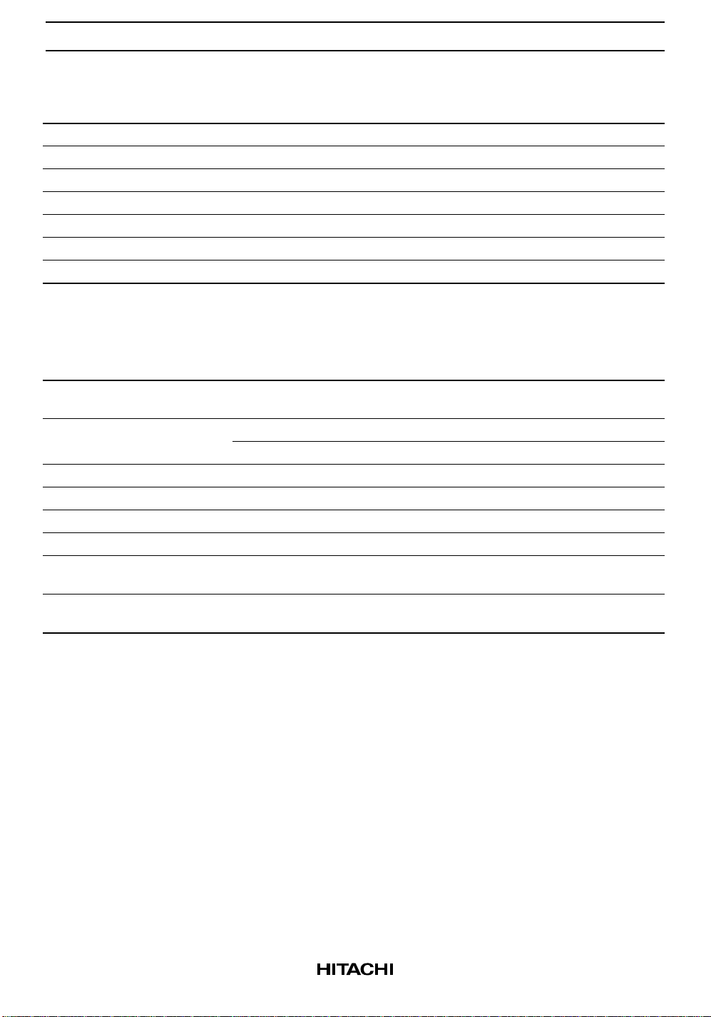
Maximum Collector Dissipation Curve
600
(mW)
C
400
200
Collector Power Dissipation P
0
50 100 150
Ambient Temperature Ta (°C)
DC Current Transfer Ratio vs.
Collector Current
200
FE
160
120
20
Typical Output Characteristic
150
16
(mA)
C
12
125
100
75
8
50
4
Collector Current I
= 25 µA
I
B
024 1086
Collector to Emitter Voltage V
CE
(V)
Gain Bandwidth Product vs.
Collector Current
10
V
= 5 V
CE
8
(GHz)
T
V
= 5 V
CE
6
80
40
DC Current Transfer Ratio h
0
12 10
Collector Current I
(mA)
C
50520
4
2
Gain Bandwidth Product f
0
12 10
Collector Current I
(mA)
C
50520
3
Page 4

2SC4422
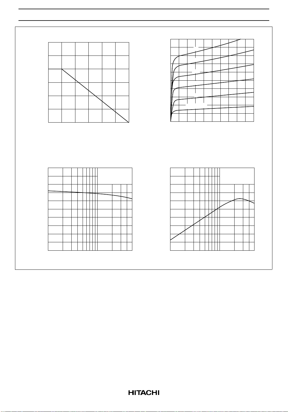
Collector Output Capacitance vs.
Collector to Base Voltage
2.0
(pF)
ob
1.6
1.2
0.8
0.4
Collector Output Capacitance C
0
1 2 10 50520
Collector to Base Voltage VCB (V)
IE = 0
f = 1 MHz
5
4
3
Power Gain vs. Collector Current
20
16
12
8
Power Gain PG (dB)
4
0
1 2 10 50520
Noise Figure vs. Collector Current
VCE = 5 V
f = 900 MHz
Collector Current I
VCE = 0
f = 900 MHz
(mA)
C
2
Noise Figure NF (dB)
1
0
1 2 10 50520
Collector Current IC (mA)
4
Page 5

S Parameters (Emitter Common)
Test Condition VCE = 5 V, 100 MHz to 1000 MHz (100 MHz Step), ZO = 50 Ω
IC = 5 mA
I
= 10 mA
C
S11-Frequency
1
0.2
0
–0.2
0.8
0.6
0.4
0.2 0.4 0.6 1 1.52 3 5 104
–0.4
–0.6
–0.8
–1
1.5
2
3
4
5
10
∞
–10
–5
–4
–3
–2
–1.5
2SC4422
–180°
150°
–150°
120°
–120°
S21-Frequency
90°
–90°
Scale : 10/div
60°
30°
0°
–30°
–60°
5
Page 6

2SC4422
120°
S12-Frequency
90°
Scale : 0.1/div
60°
–180°
0.2
0
150°
–150°
0.4
0.2 0.4 0.6
–120°
0.6
–90°
S22-Frequency
1
0.8
0.8
1 1.52 3 5 104
30°
0°
–30°
–60°
1.5
2
3
4
5
10
∞
–10
–0.2
–0.4
–0.6
–0.8
–1
–2
–1.5
–5
–4
–3
6
Page 7

2SC4422
S Parameters (Emitter Common)
Test Condition VCE = 5 V, IC = 5 mA, ZO = 50 Ω
Freq. S11 S21 S12 S22
(MHz) MAG. ANG. MAG. ANG. MAG. ANG. MAG. ANG.
100 0.747 –42.0 12.471 143.1 0.044 69.5 0.840 –24.6
200 0.534 –70.3 8.958 119.9 0.071 62.3 0.640 –36.3
300 0.394 –91.0 6.624 106.1 0.090 61.2 0.522 –40.4
400 0.310 –105.3 5.194 96.8 0.108 62.5 0.456 –42.4
500 0.258 –117.0 4.280 89.7 0.126 64.1 0.417 –43.7
600 0.216 –126.9 3.636 84.0 0.145 65.1 0.391 –45.4
700 0.193 –139.0 3.170 79.0 0.165 65.9 0.376 –47.5
800 0.167 –149.6 2.824 74.5 0.185 66.5 0.368 –50.0
900 0.157 –162.3 2.543 70.2 0.206 66.9 0.363 –53.1
1000 0.136 –171.9 2.326 66.6 0.227 67.0 0.362 –56.3
Test Condition VCE = 5 V, IC = 20 mA, ZO = 50 Ω
Freq. S11 S21 S12 S22
(MHz) MAG. ANG. MAG. ANG. MAG. ANG. MAG. ANG.
100 0.333 –71.6 21.905 117.7 0.031 71.9 0.547 –37.3
200 0.192 –98.5 12.026 100.7 0.054 74.6 0.378 –37.6
300 0.135 –116.1 8.123 92.4 0.079 75.8 0.322 –35.5
400 0.107 –130.9 6.151 86.7 0.104 76.2 0.297 –35.7
500 0.088 –145.2 4.967 82.3 0.129 75.5 0.285 –36.6
600 0.078 –155.4 4.174 78.2 0.153 74.8 0.275 –38.8
700 0.069 –170.6 3.616 74.7 0.178 73.8 0.271 –42.0
800 0.060 176.2 3.201 71.1 0.203 72.8 0.268 –45.3
900 0.063 162.6 2.876 67.9 0.227 71.7 0.268 –49.3
1000 0.051 147.4 2.624 65.0 0.251 70.5 0.271 –53.5
7
Page 8

2SC4422
Y Parameters (Emitter Common)
Test Condition VCE = 5 V, IC = 5 mA
Freq. Yie (mS) Yfe (mS) Yre (mS) Yoe (mS)
(MHz) REAL IMAG. REAL IMAG. REAL IMAG. REAL IMAG.
100 1.949 3.563 147.837 –43.785 –0.001 –0.544 0.175 0.922
200 3.994 5.961 120.026 –75.352 0.005 –1.122 0.218 1.731
300 6.433 7.295 89.506 –98.131 0.006 –1.711 0.206 2.618
400 8.206 7.536 62.937 –90.892 0.017 –2.299 0.250 3.531
500 9.403 7.501 43.528 –87.146 0.043 –2.877 0.295 4.395
600 10.179 7.259 29.375 –81.334 0.058 –3.445 0.421 5.324
700 10.910 7.124 19.483 –75.831 0.098 –4.063 0.387 6.235
800 11.193 6.776 11.803 –70.096 0.127 –4.642 0.413 7.209
900 11.543 6.593 6.205 –65.171 0.192 –5.302 0.338 8.218
1000 11.387 6.328 2.208 –60.095 0.249 –5.855 0.401 9.171
Test Condition VCE = 5 V, IC = 20 mA
Freq. Yie (mS) Yfe (mS) Yre (mS) Yoe (mS)
(MHz) REAL IMAG. REAL IMAG. REAL IMAG. REAL IMAG.
100 5.863 2.308 276.917 –268.988 0.000 –0.522 0.244 0.751
200 7.022 2.660 109.913 –221.759 0.005 –1.121 0.309 1.637
300 7.375 2.861 50.698 –167.756 0.006 –1.713 0.305 2.507
400 7.527 3.094 26.179 –133.425 0.024 –2.302 0.363 3.373
500 7.607 3.429 14.053 –110.501 0.025 –2.885 0.394 4.282
600 7.562 3.893 7.198 –94.442 0.056 –3.477 0.463 5.156
700 7.537 4.211 2.859 –82.874 0.079 –4.077 0.478 6.093
800 7.383 4.635 –0.221 –73.836 0.124 –4.674 0.506 7.046
900 7.403 5.047 –2.127 –67.183 0.180 –5.312 0.444 8.018
1000 7.074 5.411 –3.292 –61.241 0.246 –5.871 0.509 8.943
8
Page 9

Unit: mm
0.53 Max
0.48 Max
4.5 ± 0.1
1.8 Max
1.5
1.5
3.0
1.5 ± 0.1
0.4
φ
1
0.44 Max
(1.5)
(2.5)
2.5 ± 0.1
4.25 Max
0.44 Max
(0.4)
(0.2)
0.8 Min
Hitachi Code
JEDEC
EIAJ
Weight
(reference value)
UPAK
—
Conforms
0.050 g
Page 10

Cautions
1. Hitachi neither warrants nor grants licenses of any rights of Hitachi’s or any third party’s patent,
copyright, trademark, or other intellectual property rights for information contained in this document.
Hitachi bears no responsibility for problems that may arise with third party’s rights, including
intellectual property rights, in connection with use of the information contained in this document.
2. Products and product specifications may be subject to change without notice. Confirm that you have
received the latest product standards or specifications before final design, purchase or use.
3. Hitachi makes every attempt to ensure that its products are of high quality and reliability. However,
contact Hitachi’s sales office before using the product in an application that demands especially high
quality and reliability or where its failure or malfunction may directly threaten human life or cause risk
of bodily injury, such as aerospace, aeronautics, nuclear power, combustion control, transportation,
traffic, safety equipment or medical equipment for life support.
4. Design your application so that the product is used within the ranges guaranteed by Hitachi particularly
for maximum rating, operating supply voltage range, heat radiation characteristics, installation
conditions and other characteristics. Hitachi bears no responsibility for failure or damage when used
beyond the guaranteed ranges. Even within the guaranteed ranges, consider normally foreseeable
failure rates or failure modes in semiconductor devices and employ systemic measures such as failsafes, so that the equipment incorporating Hitachi product does not cause bodily injury, fire or other
consequential damage due to operation of the Hitachi product.
5. This product is not designed to be radiation resistant.
6. No one is permitted to reproduce or duplicate, in any form, the whole or part of this document without
written approval from Hitachi.
7. Contact Hitachi’s sales office for any questions regarding this document or Hitachi semiconductor
products.
Hitachi, Ltd.
Semiconductor & Integrated Circuits.
Nippon Bldg., 2-6-2, Ohte-machi, Chiyoda-ku, Tokyo 100-0004, Japan
Tel: Tokyo (03) 3270-2111 Fax: (03) 3270-5109
URL NorthAmerica : http:semiconductor.hitachi.com/
For further information write to:
Hitachi Semiconductor
(America) Inc.
179 East Tasman Drive,
San Jose,CA 95134
Tel: <1> (408) 433-1990
Fax: <1>(408) 433-0223
Europe : http://www.hitachi-eu.com/hel/ecg
Asia (Singapore) : http://www.has.hitachi.com.sg/grp3/sicd/index.htm
Asia (Taiwan) : http://www.hitachi.com.tw/E/Product/SICD_Frame.htm
Asia (HongKong) : http://www.hitachi.com.hk/eng/bo/grp3/index.htm
Japan : http://www.hitachi.co.jp/Sicd/indx.htm
Hitachi Europe GmbH
Electronic components Group
Dornacher Stra§e 3
D-85622 Feldkirchen, Munich
Germany
Tel: <49> (89) 9 9180-0
Fax: <49> (89) 9 29 30 00
Hitachi Europe Ltd.
Electronic Components Group.
Whitebrook Park
Lower Cookham Road
Maidenhead
Berkshire SL6 8YA, United Kingdom
Tel: <44> (1628) 585000
Fax: <44> (1628) 778322
Hitachi Asia Pte. Ltd.
16 Collyer Quay #20-00
Hitachi Tower
Singapore 049318
Tel: 535-2100
Fax: 535-1533
Hitachi Asia Ltd.
Taipei Branch Office
3F, Hung Kuo Building. No.167,
Tun-Hwa North Road, Taipei (105)
Tel: <886> (2) 2718-3666
Fax: <886> (2) 2718-8180
Copyright ' Hitachi, Ltd., 1999. All rights reserved. Printed in Japan.
Hitachi Asia (Hong Kong) Ltd.
Group III (Electronic Components)
7/F., North Tower, World Finance Centre,
Harbour City, Canton Road, Tsim Sha Tsui,
Kowloon, Hong Kong
Tel: <852> (2) 735 9218
Fax: <852> (2) 730 0281
Telex: 40815 HITEC HX
 Loading...