

Page 1

2SC4416
Silicon NPN Epitaxial
Application
UHF Frequency conversion, Wide band amplifier
Outline
MPAK
3
1
2
1. Base
2. Emitter
3. Collector
Page 2
2SC4416
Absolute Maximum Ratings (Ta = 25°C)
Item Symbol Ratings Unit
Collector to base voltage V
Collector to emitter voltage V
Emitter to base voltage V
Collector current I
Collector power dissipation P
CBO
CEO
EBO
C
C
Junction temperature Tj 150 °C
Storage temperature Tstg –55 to +150 °C
Electrical Characteristics (Ta = 25°C)
Item Symbol Min Typ Max Unit Test conditions
Collector to base breakdown
V
(BR)CBO
voltage
Collector cutoff current I
Emitter cutoff current I
Collector to emitter saturation
I
V
CBO
CEO
EBO
CE(sat)
voltage
DC current transfer ratio h
FE
Collector output capacitance Cob — 0.85 1.3 pF VCB = 10 V, IE = 0, f = 1 MHz
Gain bandwidth product f
T
Conversion gain CG 15 19 — dB VCC = 5 V, IC = 0.8 mA,
Noise figure NF — 8 1.2 dB
Note: Marking is “XB–”.
25——V I
— — 0.1 µAVCB = 15 V, IE = 0
——10µAVCB = 13 V, RBE = ∞
— — 0.3 µAVEB = 3 V, IC = 0
— — 0.3 V IC = 20 mA, IB = 4 mA
50 — 180 VCE = 5 V, IC = 5 mA
3.0 3.8 — GHz VCE = 5 V, IC = 20 mA
25 V
13 V
3V
50 mA
150 mW
= 10 µA, IE = 0
C
f
= 900 MHz,
in
f
= 930 MHz (–5dBm),
OSC
f
= 30 MHz
out
2
Page 3
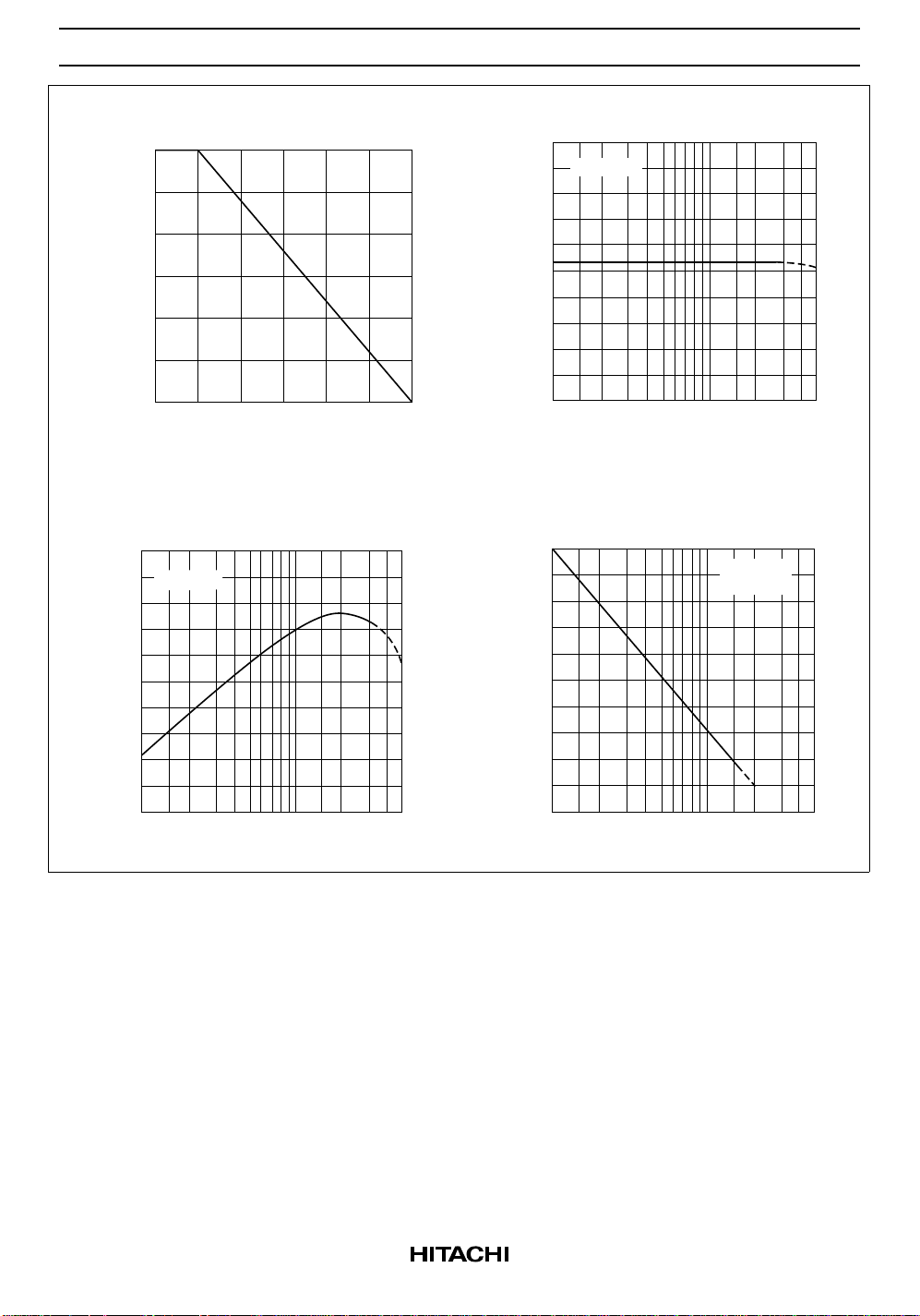
Maximum Collector Dissipation Curve
150
(mW)
C
2SC4416
DC Current Transfer Ratio vs.
Collector Current
200
FE
VCE = 5 V
160
100
50
Collector Power Dissipation P
0
15010050
Ambient Temperature Ta (°C)
Gain Bandwidth Product vs.
Collector Current
5
VCE = 5 V
4
(GHz)
T
3
2
1
Gain Bandwidth Product f
0
152021050
Collector Current I
(mA)
C
120
80
40
DC Current Transfer Ratio h
0
Collector Current I
(mA)
C
Collector Output Capacitance vs.
Collector to Base Voltage
1.2
(pF)
ob
1.1
IE = 0
f = 1 MHz
1.0
0.9
0.8
Collector Output Capacitance C
0.7
12 1052050
Collector to Base Voltage V
CB
(V)
502010521
3
Page 4

2SC4416
Conversion Gain and Noise Figure
vs. Supply Voltage
25
20
15
10
5
Conversion Gain CG (dB)
Noise Figure NF (dB)
0
12 510
Supply Voltage V
IC = 0.8 mA
f = 900 MHz
CG
NF
f
= 30 MHz
out
f
= 930 MHz(–5 dBm)
osc
(V)
CC
25
20
Conversion Gain and Noise Figure
25
VCC = 3 V
f = 900 MHz
20
15
10
5
Conversion Gain CG (dB)
Noise Figure NF (dB)
0
0.1 0.2 2 50.5 1.0
Conversion Gain and Noise Figure
vs. Collector Current
VCC = 5 V
f = 900 MHz
CG
vs. Collector Current
f
= 30 MHz
out
f
= 930 MHz(–5 dBm)
osc
Collector Current I
(mA)
C
CG
NF
15
10
5
Conversion Gain CG (dB)
Noise Figure NF (dB)
0
0.1 0.2 2 50.5 1.0
Collector Current I
NF
f
= 30 MHz
out
f
= 930 MHz(–5 dBm)
osc
(mA)
C
4
Page 5

S Parameters (Emitter Common)
Test Condition VCE = 5 V, 100 MHz to 1000 MHz (100 MHz STEP) , ZO = 50 Ω
IC = 5 mA
I
= 10 mA
C
2SC4416
0.2
0
–0.2
S11-Frequency
1
0.8
0.6
0.4
0.2 0.4 0.6 0.8 1 2 3 4 5 10
–0.4
–0.6
–0.8
S12-Frequency
120°
150°
1.5
–1
90°
1.5
–1.5
2
3
4
5
–5
–4
–3
–2
Scale : 0.4/div
60°
10
∞
–10
30°
–180°
0.2
150°
–150°
0.4
120°
–120°
0.6
S21-Frequency
90°
–90°
S22-Frequency
1
0.8
Scale : 2.5/div
60°
30°
0°
–30°
–60°
1.5
2
3
4
5
–180°
–150°
–120°
–90°
–60°
–30°
10
0
0°
–0.2
0.2 0.4 0.6 0.8 1 2 3 4 5 10
–0.4
–0.6
–0.8
–1
1.5
∞
–10
–5
–4
–3
–2
–1.5
5
Page 6

2SC4416
S Parameters (Emitter Common)
Test Condition VCE = 5 V, IC = 5 mA, ZO = 50 Ω
Freq. S11 S21 S12 S22
(MHz) MAG. ANG. MAG. ANG. MAG. ANG. MAG. ANG.
100 0.777 –47.6 12.318 146.4 0.037 66.8 0.878 –20.1
200 0.636 –82.6 9.212 124.5 0.058 55.3 0.702 –30.7
300 0.540 –107.9 6.901 110.6 0.071 51.0 0.586 –34.8
400 0.494 –125.0 5.480 101.6 0.079 50.7 0.520 –36.4
500 0.468 –138.0 4.547 94.5 0.087 52.0 0.480 –37.2
600 0.452 –147.7 3.859 89.0 0.095 53.7 0.452 –38.4
700 0.439 –155.4 3.374 84.2 0.103 55.7 0.436 –39.9
800 0.437 –162.0 2.982 80.0 0.112 57.5 0.427 –41.3
900 0.428 –167.9 2.691 76.1 0.122 59.6 0.419 –43.4
1000 0.429 –173.8 2.457 72.5 0.131 61.2 0.415 –45.0
Test Condition VCE = 5 V, IC = 10 mA, ZO = 50 Ω
Freq. S11 S21 S12 S22
(MHz) MAG. ANG. MAG. ANG. MAG. ANG. MAG. ANG.
100 0.627 –64.8 17.938 135.2 0.032 63.2 0.766 –27.4
200 0.492 –102.5 11.621 113.8 0.047 56.4 0.560 –35.3
300 0.432 –125.3 8.190 102.4 0.058 57.2 0.460 –36.1
400 0.411 –139.4 6.332 95.1 0.069 59.6 0.412 –36.2
500 0.395 –150.3 5.168 89.5 0.079 61.7 0.385 –36.2
600 0.394 –157.4 4.350 84.8 0.090 63.7 0.366 –36.8
700 0.392 –163.5 3.784 80.9 0.102 65.2 0.356 –38.3
800 0.390 –168.7 3.333 77.1 0.113 66.5 0.351 –39.7
900 0.388 –173.1 2.995 73.8 0.127 67.3 0.347 –41.6
1000 0.387 –177.0 2.731 70.5 0.138 67.9 0.345 –43.5
6
Page 7

2SC4416
Y Parameters (Emitter Common)
Test Condition VCE = 5 V, IC = 5 mA
Freq. Yie (mS) Yfe (mS) Yre (mS) Yoe (mS)
(MHz) REAL IMAG. REAL IMAG. REAL IMAG. REAL IMAG.
100 2.182 5.286 149.226 –28.448 –0.004 –0.459 0.069 0.745
200 4.596 9.838 138.489 –53.561 –0.005 –0.941 0.137 1.465
300 8.314 13.395 121.525 –74.164 –0.025 –1.460 0.086 2.251
400 12.329 15.566 103.171 –87.811 –0.044 –1.955 0.111 3.025
500 16.310 16.548 83.990 –97.188 –0.068 –2.451 0.080 3.813
600 19.817 16.562 66.015 –100.594 –0.104 –2.958 0.154 4.618
700 22.727 15.707 49.791 –101.015 –0.136 –3.433 0.226 5.461
800 25.355 14.778 36.105 –98.928 –0.165 –3.943 0.246 6.241
900 27.058 13.073 23.869 –95.428 –0.192 –4.438 0.307 7.067
1000 28.966 11.370 13.481 –92.170 –0.260 –4.944 0.328 7.902
Test Condition VCE = 5 V, IC = 10 mA
Freq. Yie (mS) Yfe (mS) Yre (mS) Yoe (mS)
(MHz) REAL IMAG. REAL IMAG. REAL IMAG. REAL IMAG.
100 4.137 6.218 246.938 –82.680 –0.004 –0.462 0.139 0.754
200 7.995 10.306 193.805 –128.092 –0.015 –0.937 0.220 1.578
300 12.296 12.125 140.844 –144.955 –0.027 –1.432 0.322 2.338
400 15.691 12.521 100.830 –145.272 –0.024 –1.913 0.404 3.028
500 18.471 12.026 70.237 –139.959 –0.049 –2.396 0.410 3.817
600 20.418 11.618 48.828 –130.672 –0.032 –2.894 0.492 4.460
700 21.855 10.887 33.158 –121.649 –0.024 –3.394 0.474 5.196
800 23.059 10.127 20.494 –112.454 –0.017 –3.889 0.502 5.950
900 23.687 9.375 11.528 –103.839 –0.013 –4.418 0.446 6.699
1000 24.366 8.807 4.277 –96.921 –0.013 –4.905 0.471 7.486
7
Page 8

2SC4416
,
Conversion Gain and Noise Figure Test Circuit
f
= 930 MHz
osc
(–5 dBm)
D
1
D1 : 1SV188
L
1
L
3
f
= 900 MHz
in
Tin
V
BB
V
1 k 2.2 n
2.2 n
L
2
8 p
100
47 p
1 k
2.2 n
D
1
2.2 n
25
47 k
2.2 n
V
Tout
V
CC
220 µ
100 p
100 p
f
= 30 MHz
out
R
= 50 Ω
L
Unit R :
C :
L :
Ω
F
H
: φ1 mm Enameled Copper Wire.
L
1
10
10
10
L
: φ1 mm Enameled Copper Wire.
2
25
10
15
30
: φ1 mm Enameled Copper Wire.
L
3
L
: Inside Dia 3 mm, φ0.5 mm Enameled Copper Wire 1 Turn.
4
10
10
Unit : mm
L5 : Inside Dia 5 mm Bobin, φ0.2 mm Enameled Copper Wire 20 Turns Using Ferrite Core.
8
Page 9

Unit: mm
3 – 0.4
+ 0.10
– 0.05
0.95
1.9 ± 0.2
2.95 ± 0.2
0.95
0.65
+ 0.2
1.5 ± 0.15
0.65
0.3
+ 0.2
– 0.6
2.8
– 0.1
1.1
+ 0.10
0.16
– 0.06
0 – 0.1
Hitachi Code
JEDEC
EIAJ
Weight
(reference value)
MPAK
—
Conforms
0.011 g
Page 10

Cautions
1. Hitachi neither warrants nor grants licenses of any rights of Hitachi’s or any third party’s patent,
copyright, trademark, or other intellectual property rights for information contained in this document.
Hitachi bears no responsibility for problems that may arise with third party’s rights, including
intellectual property rights, in connection with use of the information contained in this document.
2. Products and product specifications may be subject to change without notice. Confirm that you have
received the latest product standards or specifications before final design, purchase or use.
3. Hitachi makes every attempt to ensure that its products are of high quality and reliability. However,
contact Hitachi’s sales office before using the product in an application that demands especially high
quality and reliability or where its failure or malfunction may directly threaten human life or cause risk
of bodily injury, such as aerospace, aeronautics, nuclear power, combustion control, transportation,
traffic, safety equipment or medical equipment for life support.
4. Design your application so that the product is used within the ranges guaranteed by Hitachi particularly
for maximum rating, operating supply voltage range, heat radiation characteristics, installation
conditions and other characteristics. Hitachi bears no responsibility for failure or damage when used
beyond the guaranteed ranges. Even within the guaranteed ranges, consider normally foreseeable
failure rates or failure modes in semiconductor devices and employ systemic measures such as failsafes, so that the equipment incorporating Hitachi product does not cause bodily injury, fire or other
consequential damage due to operation of the Hitachi product.
5. This product is not designed to be radiation resistant.
6. No one is permitted to reproduce or duplicate, in any form, the whole or part of this document without
written approval from Hitachi.
7. Contact Hitachi’s sales office for any questions regarding this document or Hitachi semiconductor
products.
Hitachi, Ltd.
Semiconductor & Integrated Circuits.
Nippon Bldg., 2-6-2, Ohte-machi, Chiyoda-ku, Tokyo 100-0004, Japan
Tel: Tokyo (03) 3270-2111 Fax: (03) 3270-5109
URL NorthAmerica : http:semiconductor.hitachi.com/
For further information write to:
Hitachi Semiconductor
(America) Inc.
179 East Tasman Drive,
San Jose,CA 95134
Tel: <1> (408) 433-1990
Fax: <1>(408) 433-0223
Europe : http://www.hitachi-eu.com/hel/ecg
Asia (Singapore) : http://www.has.hitachi.com.sg/grp3/sicd/index.htm
Asia (Taiwan) : http://www.hitachi.com.tw/E/Product/SICD_Frame.htm
Asia (HongKong) : http://www.hitachi.com.hk/eng/bo/grp3/index.htm
Japan : http://www.hitachi.co.jp/Sicd/indx.htm
Hitachi Europe GmbH
Electronic components Group
Dornacher Stra§e 3
D-85622 Feldkirchen, Munich
Germany
Tel: <49> (89) 9 9180-0
Fax: <49> (89) 9 29 30 00
Hitachi Europe Ltd.
Electronic Components Group.
Whitebrook Park
Lower Cookham Road
Maidenhead
Berkshire SL6 8YA, United Kingdom
Tel: <44> (1628) 585000
Fax: <44> (1628) 778322
Hitachi Asia Pte. Ltd.
16 Collyer Quay #20-00
Hitachi Tower
Singapore 049318
Tel: 535-2100
Fax: 535-1533
Hitachi Asia Ltd.
Taipei Branch Office
3F, Hung Kuo Building. No.167,
Tun-Hwa North Road, Taipei (105)
Tel: <886> (2) 2718-3666
Fax: <886> (2) 2718-8180
Copyright ' Hitachi, Ltd., 1999. All rights reserved. Printed in Japan.
Hitachi Asia (Hong Kong) Ltd.
Group III (Electronic Components)
7/F., North Tower, World Finance Centre,
Harbour City, Canton Road, Tsim Sha Tsui,
Kowloon, Hong Kong
Tel: <852> (2) 735 9218
Fax: <852> (2) 730 0281
Telex: 40815 HITEC HX
 Loading...