

Page 1
SHINDENGEN
Switching Power Transistor
2SC4059
(T15W45FX)
15A NPN
FX Series
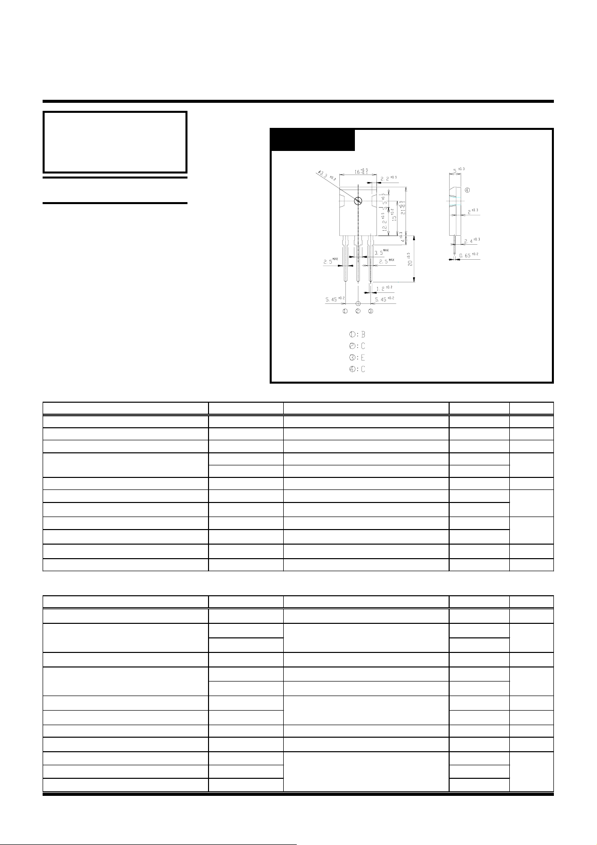
OUTLINE DIMENSIONS
Case : MTO-3P
Unit : mm
RATINGS
●Absolute Maximum Ratings
Item Symbol
Storage Temperature
Junction Temperature
Collector to Base Voltage
Collector to Emitter Voltage
Emitter to Base Voltage
Collector Current DC
Collector Current Peak
Base Current DC
Base Current Peak
Total Transistor Dissipation
Mounting Torque
●Electrical Characteristics (Tc=25℃)
Item Symbol
Collector to Emitter Sustaining Voltage
Collector Cutoff Current
Emitter Cutoff Current
DC Current Gain
Collector to Emitter Saturation Voltage
Base to Emitter Saturation Voltage
Thermal Resistance
Transition Frequency
Turn on Time
Storage Time
Fall Time
Conditions
Ratings Unit
Tstg -55~150 ℃
Tj 150 ℃
V
CBO
V
CEO
V
CEX
V
EBO
I
C
I
CP
I
B
I
BP
P
T
VEB = 5V
Tc = 25℃
600 V
450 V
600
7V
15A
30
6
12
130
TOR 0.8
V
(sus)
CEO
I
CBO
I
CEO
I
EBO
h
FE
h
FEL
VCE(sat)
VBE(sat)
θjc
f
T
ton
ts
tf
Conditions
IC = 0.2A
At rated Voltage
At rated Voltage
V
= 5V, IC = 7.5A
CE
V
= 5V, IC = 1mA
CE
IC = 7.5A
IB = 1.5A
Junction to case
V
= 10V, IC = 1.5A
CE
IC = 7.5A
IB1 = 1.5A, IB2 = 3A
RL = 20Ω, V
BB2
= 4V
Ratings Unit
Min 450 V
Max 0.1 mA
Max 0.1
Max 0.1 mA
Min 10
Min 5
Max 1.0 V
Max 1.5 V
Max 0.96 ℃/W
STD 20 MHz
Max 0.5
Max 2.0 μs
Max 0.2
A
W
N・m
Copyright & Copy;2000 Shindengen Electric Mfg.Co.Ltd
Page 2

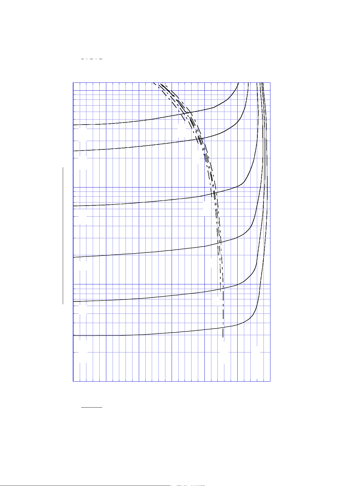
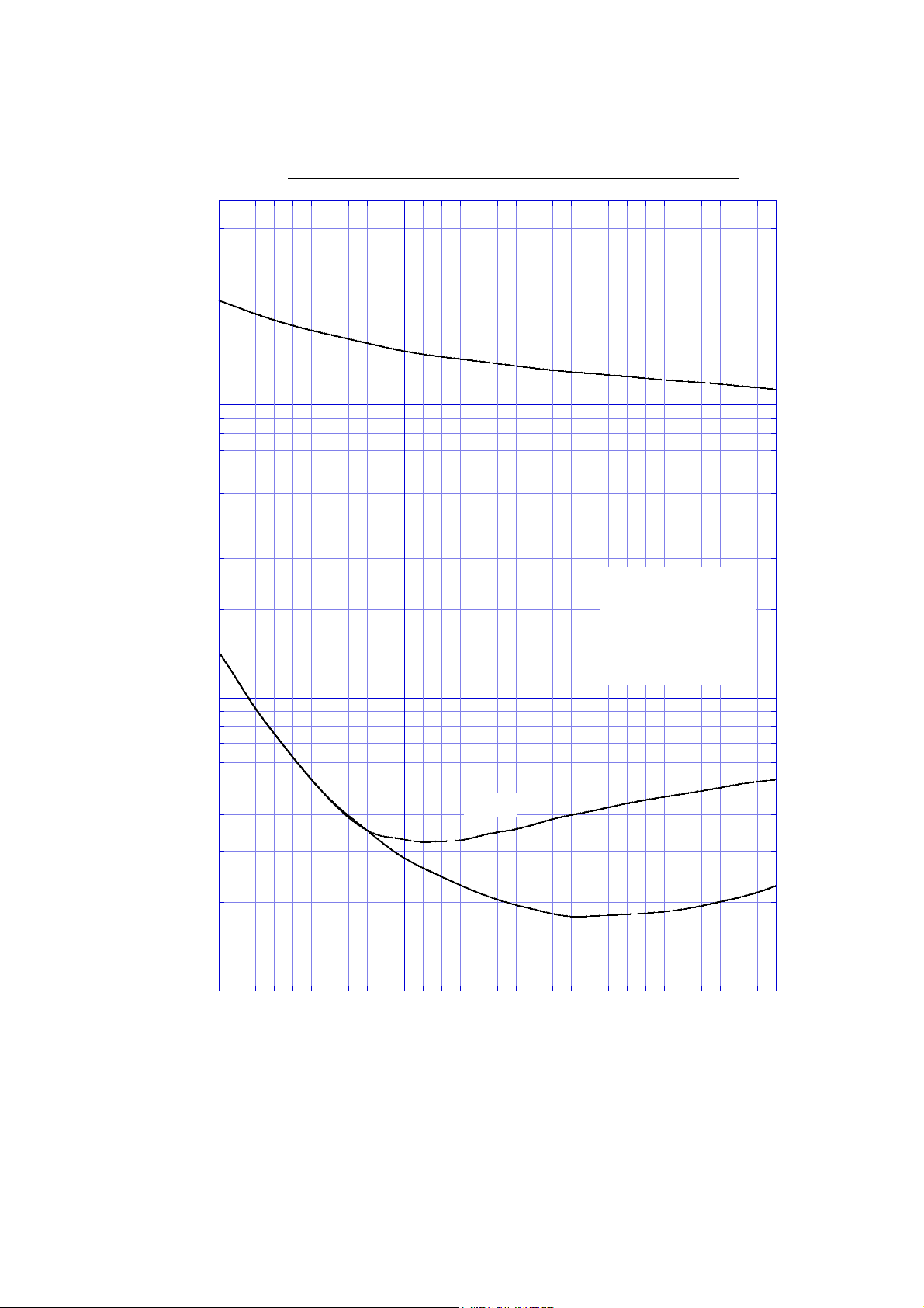
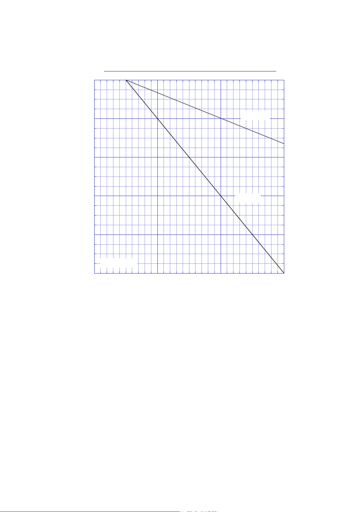
C
- I
FE
h
= 5V
CE
V
30
[A]
C
2SC4059
100
Tc = 150°C
100°C
FE
50°C
25°C
0°C
−25°C
10
−55°C
1
DC Current Gain h
Collector Current I
0.001 0.01 0.1 1 10
Page 3
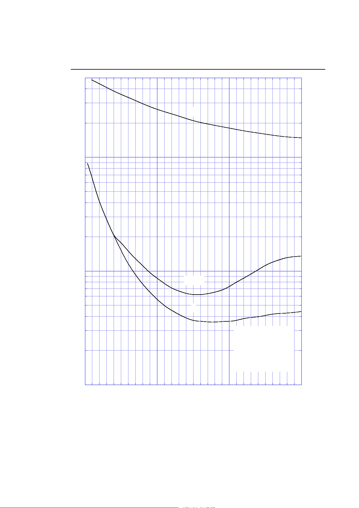
BE
[V]
Base-Emitter Voltage V
3
2.5
Saturation Voltage
2
1.5
20A
1
15A
7.5A
0.5
0
12
[A]
B
2SC4059
= 1A 2A 4A 7.5A 15A 20A
C
I
3
2.5
CE
[V]
4A
2A
= 1A
C
I
Tc = 25°C
0.01 0.1 1 10
2
1.5
1
0.5
0
Base Current I
Collector-Emitter Voltage V
Page 4

[µs]
SW
2SC4059
1
Switching Time - I
t
s
t
on
C
0.1
Switching Time t
0.01
0 5 10 15
t
f
Collector Current IC [A]
IB1 = 0.2I
IB2 = 0.4I
V
BB2
VCC = 150V
Tc = 25°C
C
C
= 4V
Page 5
2SC4059
1
Switching Time - V
t
s
CC
[µs]
SW
0.1
Switching Time t
t
on
t
f
IC = 7.5A
IB1 = 1.5A
IB2 = 3.0A
V
= 4V
BB2
Tc = 25°C
0.01
0 50 100 150 200 250 300
Collector Voltage VCC [V]
Page 6
[µs]
SW
2SC4059
1
Switching Time - Tc
t
s
t
on
0.1
Switching Time t
0.01
0 50 100 150
t
f
IC = 7.5A
IB1 = 1.5A
IB2 = 3.0A
V
R
Case Temperature Tc [°C]
= 4V
BB2
= 20Ω
L
Page 7
[µs]
SW
2SC4059
L-Load Switching Time - I
t
s
C
1
0.1
Switching Time t
0.01
0 5 10 15
tf + t
t
f
vs
IB1 = 0.2I
IB2 = 0.4I
V
= 4V
BB2
V
CE (clamp)
Tc = 25°C
C
C
= 300V
Collector Current IC [A]
Page 8
2SC4059
1
[µs]
SW
L-Load Switching Time - IC (At High Temperature)
t
s
0.1
Switching Time t
0.01
0 5 10 15
tf + t
vs
t
f
IB1 = 0.2I
IB2 = 0.4I
V
V
Tc = 100°C
Collector Current IC [A]
= 4V
BB2
CE (clamp)
C
C
= 300V
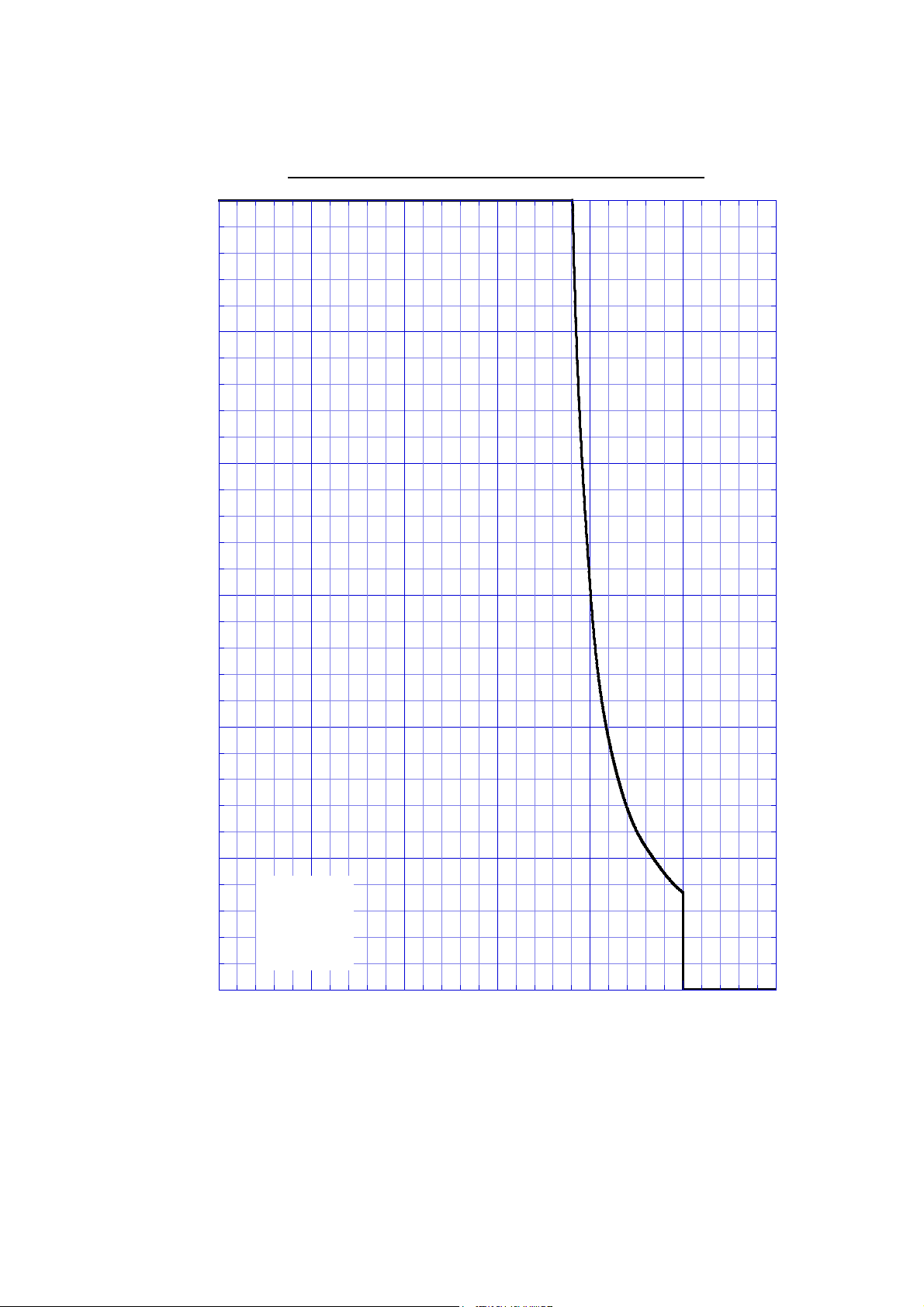
Page 9
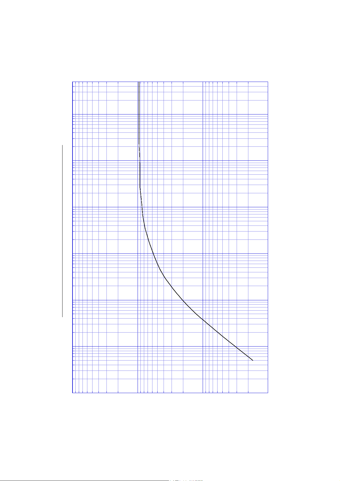
1
10
0
10
-1
10
Transient Thermal Impedance
2SC4059
10
1
0.1
-2
Time t [s]
10
-3
10
-4
10
-5
10
0.01
Transient Thermal Impedance θjc(t) [°C/W]
Page 10
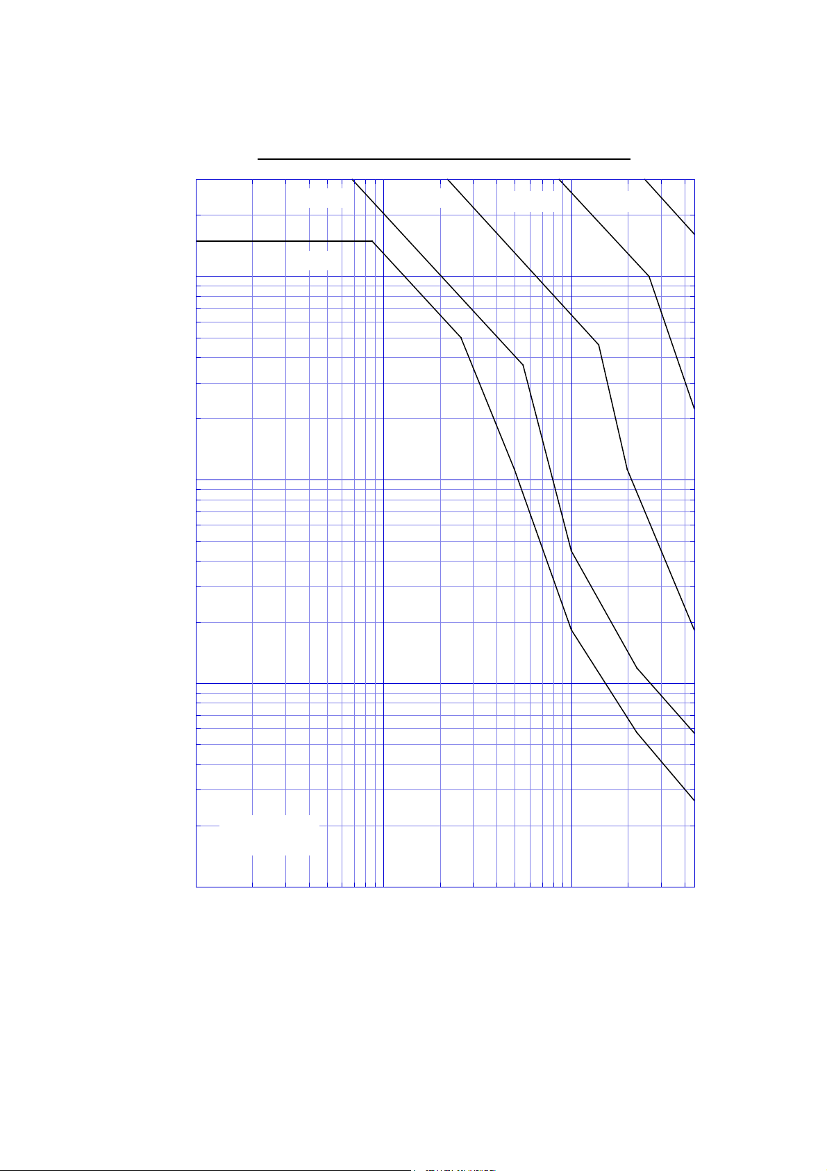
30
15
10
[A]
C
2SC4059
DC
1
Forward Bias SOA
1ms10ms
150µs
50µs
Collector Current I
0.1
Tc = 25°C
Single Pulse
0.01
1 10 100
Collector-Emitter Voltage VCE [V]
450
Page 11
100
80
60
2SC4059 Collector Current Derating
I
limit
S/B
40
Collector Current Derating [%]
20
VCE = fixed
0
0 50 100 150
PT limit
Case Temperature Tc [°C]
Page 12
30
25
20
[A]
C
15
2SC4059
Reverse Bias SOA
Collector Current I
10
5
IB1 = 0.3I
IB2 = 4.5A
V
BB2
Tc < 150°C
0
0 100 200 300 400 500 600
C
= 5V
Collector-Emitter Voltage VCE [V]
 Loading...