

Page 1
DATA SHEET
SILICON TRANSISTOR
NPN EPITAXIAL SILICON TRANSISTOR
FOR MICROWAVE LOW-NOISE AMPLIFICATION
2SC3604
The 2SC3604 is an NPN epitaxial transistor designed for lownoise amplification at 1.0 to 6.0 GHz. This transistor has low-noise
and high-gain characteristics in a wide collector current region, and
has a wide dynamic range.
FEATURES
• Low noise : NF = 1.6 dB TYP. @ f = 2.0 GHz
• High power gain: G
ABSOLUTE MAXIMUM RATINGS (TA = 25
PARAMETER SYMBOL RATING UNIT
Collector to Base Voltage VCBO 20 V
Collector to Emitter Voltage VCEO 10 V
Emitter to Base Voltage VEBO 1.5 V
Collector Current IC 65 mA
Total Power Dissipation PT (TC = 25 °C) 580 mW
Junction Temperature Tj 200 °C
Storage Temperature Tstg
A = 12 dB TYP. @ f = 2.0 GHz
°°
°C)
°°
-
65 to +150 °C
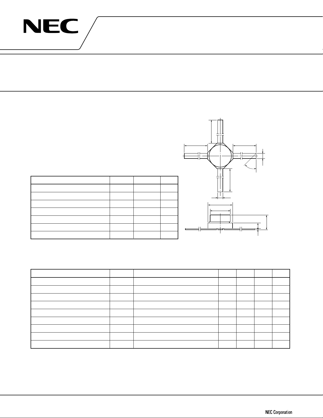
PACKAGE DIMENSIONS (in mm)
E
3.8 MIN.
3.8 MIN.
CB
E
2.55 ± 0.2
2.1
φ
3.8 MIN.
3.8 MIN.
0.5 ± 0.05
0.5 ± 0.05
45 °
PIN CONNECTIONS
E: Emitter
C: Collector
B: Base
0.55
1.8 MAX.
+0.06
-0.03
0.1
ELECTRICAL CHARACTERISTICS (TA = 25
PARAMETER SYMBOL TEST CONDITIONS MIN. TYP. MAX. UNIT
Collector Cut-off Current ICBO VCB = 10 V, IE = 0 1.0
Emitter Cut-off Current IEBO VEB = 1 V, IC = 0 1.0
DC Current Gain hFE VCE = 8 V, IC = 20 mA Pulse 50 100 250
Gain Bandwidth Product fT VCE = 8 V, IC = 20 mA 8 GHz
Reverse Transfer Capacitance Cre VCB = 10 V, IE = 0, f = 1 MHz 0.2 0.7 pF
Noise Figure NF
Insertion Gain |S21e|2VCE = 8 V, IC = 20 mA, f = 2.0 GHz 9.0 11 dB
Maximum Available Gain MAG VCE = 8 V, IC = 20 mA, f = 2.0 GHz 13 dB
Power Gain GA VCE = 8 V, IC = 7 mA, f = 2.0 GHz 12 dB
Document No. P11675EJ2V0DS00 (2nd edition)
Date Published August 1996 P
Printed in Japan
Note
°°
°C)
°°
VCE = 8 V, IC = 7 mA, f = 2.0 GHz 1.6 2.3 dB
©
µ
A
µ
A
1996
Page 2
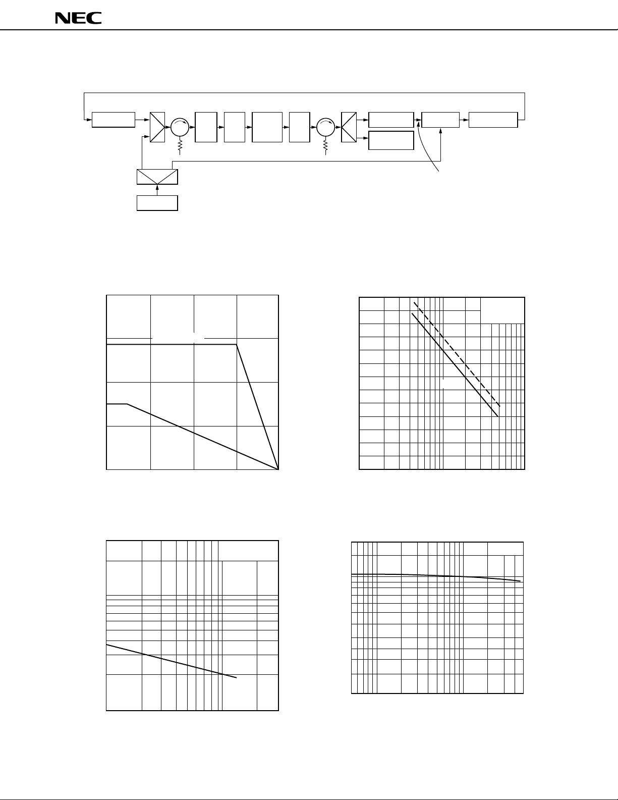
Note Test block diagram
Coax. SW Coax. SW
Noise Diode
Stub
Tuner
Bias
Tee
Transistor
Under
Test
Bias
Tee
Post Amp Mixer
Network
Analyzer
2SC3604
NF Meter
Coax. SW
Sweeper
TYPICAL CHARACTERISTICS (TA = 25
TOTAL POWER DISSIPATION vs.
AMBIENT TEMPERATURE
0.8
0.6
0.4
0.2
- Total Power Dissipation - W
T
P
0
with heat sink
R
th(j−e)
90 °C/W
th(j−a)
R
590 °C/W
50 100
A
- Ambient Temperature - °C
T
150 0.1
°°
°C)
°°
*
To test 1 GHz or lower, insert a bandpass filter.
*
MAG AND INSERTION GAIN vs.
FREQUENCY
25
20
15
10
5
- Insertion Gain - dB
2
|
21e
0
MAG - Maximum Available Gain - dB
|S
−5
0.2 0.5 1
f - Frequency - GHz
MAG
|S
21e
2
|
CE
= 8 V
V
I
C
= 20 mA
2510200
REVERSE TRANSFER CAPACITANCE vs.
COLLECTOR TO BASE VOLTAGE
3
2
1
0.7
0.5
0.3
0.2
- Reverse Transfer Capacitance - pF
re
C
0.1
1235
V
CB
- Collector to Base Voltage -V
2
f = 1.0 MHz
710 2030
DC CURRENT GAIN vs.
COLLECTOR CURRENT
200
100
50
- DC Current Gain
FE
h
20
10
0.5 1 5
I
C
- Collector Current - mA
V
CE
= 8 V
10 50
Page 3
2SC3604
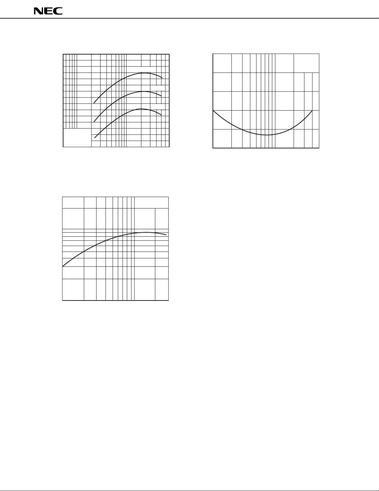
INSERTION GAIN vs.
15
10
- Insertion Gain - dB
2
5
|
21e
|S
V
CE
0
0.5 1
30
20
COLLECTOR CURRENT
= 8 V
IC - Collector Current - mA
GAIN BANDWIDTH PRODUCT vs.
COLLECTOR CURRENT
f = 2 GHz
5
10 50 70
V
CE
= 8 V
3 GHz
4 GHz
NOISE FIGURE vs. COLLECTOR CURRENT
6
5
4
3
NF - Noise Figure -dB
2
1
2 5 10 20 50
IC - Collector Current - mA
VCE = 8 V
f = 2 GHz
10
7
5
3
2
- Gain Bandwidth Product - GHz
T
f
12357102030
IC - Collector Current - mA
S PARAMETER
CE = 6 V, IC = 10 mA, ZO = 50 Ω
V
f (MHz) |S
500 .463
1000 .432
11| ∠S11 |S21| ∠S21 |S12| ∠S12 |S22| ∠S22
-
125.3 13.822 106.8 .027 37.9 .516
-
162.7 7.901 86.2 .0424 48.2 .463
1500 .416 178.7 5.250 71.1 .0606 53.1 .421
2000 .439 165.0 3.949 59.7 .0758 52.0 .396
2500 .451 153.6 3.151 51.7 .097 49.3 .372
3000 .470 143.6 2.809 39.6 .111 45.1 .345
3500 .482 135.2 2.337 28.6 .124 39.5 .320
4000 .494 129.1 2.022 21.3 .132 35.5 .321
-
-
-
-
-
-
-
-
36.6
40.7
46.2
50.9
56.5
63.7
73.2
82.0
3
Page 4

S PARAMETER
2SC3604
S
11e
, S
22e
− FREQUENCY VCE = 8 V
0.09
0.08
0.42
120
0.07
0.43
130
0.06
0.05
0.45
R
0.04
O
T
0.46
A
150
L
E
N
E
G
0.03
D
R
R
W
O
T
0.02
S
H
T
G
N
E
L
E
0.01
V
A
W
0
0
0.49
0.48
E
0.47
0.2
M
S
E
E
R
G
E
0.48
D
N
I
0.1
T
N
E
I
C
I
0.49
F
F
E
O
C
0
N
O
I
T
C
E
L
D
F
A
E
O
R
0.01
L
F
0.1
D
O
R
E
A
L
W
G
O
N
T
0.02
A
S
T
H
N
T
160
E
0.2
G
-
N
E
0.03
L
E
0.47
V
A
W
150
-
0.04
0.46
0.05
0.45
0.5
T
0.44
A
G
0.1
N
O
0.3
0.44
N
E
N
O
P
M
O
140
0.4
C
E
C
N
A
T
C
O
A
+JX
Z
0.3
E
R
E
V
I
T
0.2
0.3
S
11e
P
M
O
C
E
C
N
O
A
Z
T
JX
C
-
A
E
R
E
V
I
T
0.4
140
A
-
G
E
M
0.06
0.5
130
-
0.07
0.43
0.08
0.42
0.10
0.40
0.41
110
0.7
0.6
4 GHz
0.4
0.5
RESTSTANCE COMPONENT
0.5 GHz
0.6
120
-
0.7
110
-
0.09
0.41
0.40
0.11
0.39
0.6
0.8
0.10
0.13
0.12
0.35
100
0.9
0.8
0.7
0.8
R
ZO
0.9
100
-
0.11
0.39
90
1.0
0.9
1.0
4 GHz
1.0
0.12
0.38
0.14
0.37
0.2
0.4
0.2
0.2
0.4
-
90
0.15
0.36
80
1.2
0.6
0.8
1.0
0.8
0.6
0.4
1.2
1.4
0.6
0.8
1.0
0.8
0.6
0.4
0.2
1.2
-
80
0.13
0.37
1.0
1.6
0.14
1.8
1.0
S
22e
0.36
0.35
70
1.4
2.0
0.5 GHz
1.4
-
70
0.15
0.35
0.16
0.34
0.17
0.33
60
1.8
2.0
3.0
4.0
2.0
1.8
-
1.6
60
0.16
0.34
0.18
0.32
50
5.0
-
50
0.18
0.17
0.33
I
C
= 20 mA
500 MHz Step
0.19
0.31
0.20
40
0.30
0.21
3.0
0.29
30
4.0
0.28
20
5.0
10
10
20
50
102050
50
20
-
10
10
-
20
0.22
5.0
4.0
-
0.21
30
0.29
3.0
0.20
-
0.30
40
0.19
0.31
0.32
0.22
0.23
0.27
0.24
0.26
0.25
0.25
0
0.24
0.26
0.23
0.27
0.28
180°
150°
−150°
S
21e
− FREQUENCY
120°
−120°
0.5 GHz
90°
−90°
150°
−150°
S
12e
− FREQUENCY
120°
−120°
90°
VCC = 8 V
I
C
= 20 mA
500 MHz Step
60°
30°
4 GHz
5 0.10.05
−60°
0°
10
180°
−30°
−90°
VCE = 8 V
I
500 MHz Step
0.5 GHz
C
= 20 mA
60°
−60°
4 GHz
30°
0°
−30°
4
Page 5

2SC3604
MARKING
Because the package of the micro X package transistor is too small to be marked, the following indication is
employed.
Part Number
Part Number Marking Part Number Marking
2SC2148 A 2SC3603 0
2SC2149 B 2SC3604 2
2SC2150 C 2SC3587 1
2SC2367 H
2SC2585 K
2SC1223 D
CB
Part number
E
Aa
Lot
E
Lot
Lot indication is colored as shown below.
The sequence black, brown, red, blue, and green, forms one cycle and this cycle is repeated.
Year
Month
1 j Black v h t f r d p b
2kwiugseqc
3lxjvhtfrd
4my kw i u g s e
5nzlxjvhtf
6 o a Brown m y k w i u g
7pbnz l x j vh
8 q c o a Red m y k w i
9rdpbnzlx j
10 s e q c o a Blue m y k
11 t f r d p b n z l
12 u g s e q c o a Green m
1988 1989 1990 1991 1992 1993 1994 1995 1996
5
Page 6

[MEMO]
2SC3604
6
Page 7

[MEMO]
2SC3604
7
Page 8

2SC3604
The export of this product from Japan is prohibited without governmental license. To export or re-export this product from
a country other than Japan may also be prohibited without a license from that country. Please call an NEC sales
representative.
No part of this document may be copied or reproduced in any form or by any means without the prior written
consent of NEC Corporation. NEC Corporation assumes no responsibility for any errors which may appear in this
document.
NEC Corporation does not assume any liability for infringement of patents, copyrights or other intellectual
property rights of third parties by or arising from use of a device described herein or any other liability arising
from use of such device. No license, either express, implied or otherwise, is granted under any patents,
copyrights or other intellectual property rights of NEC Corporation or others.
While NEC Corporation has been making continuous effort to enhance the reliability of its semiconductor devices,
the possibility of defects cannot be eliminated entirely. To minimize risks of damage or injury to persons or
property arising from a defect in an NEC semiconductor device, customer must incorporate sufficient safety
measures in its design, such as redundancy, fire-containment, and anti-failure features.
NEC devices are classified into the following three quality grades:
“Standard“, “Special“, and “Specific“. The Specific quality grade applies only to devices developed based on
a customer designated “quality assurance program“ for a specific application. The recommended applications
of a device depend on its quality grade, as indicated below. Customers must check the quality grade of each
device before using it in a particular application.
Standard: Computers, office equipment, communications equipment, test and measurement equipment,
audio and visual equipment, home electronic appliances, machine tools, personal electronic
equipment and industrial robots
Special: Transportation equipment (automobiles, trains, ships, etc.), traffic control systems, anti-disaster
systems, anti-crime systems, safety equipment and medical equipment (not specifically designed
for life support)
Specific: Aircrafts, aerospace equipment, submersible repeaters, nuclear reactor control systems, life
support systems or medical equipment for life support, etc.
The quality grade of NEC devices in “Standard“ unless otherwise specified in NEC's Data Sheets or Data Books.
If customers intend to use NEC devices for applications other than those specified for Standard quality grade,
they should contact NEC Sales Representative in advance.
Anti-radioactive design is not implemented in this product.
M4 94.11
6
 Loading...