

Page 1
Ordering number:EN1392A
PNP/NPN Epitaxial Planar Silicon Transistors
2SA1339/2SC3393
High-Speed Switching Applications
Features
· Very small-sized package permitting sets to be smallsized, slim.
· High breakdown voltage : V
CEO
=(–)50V.
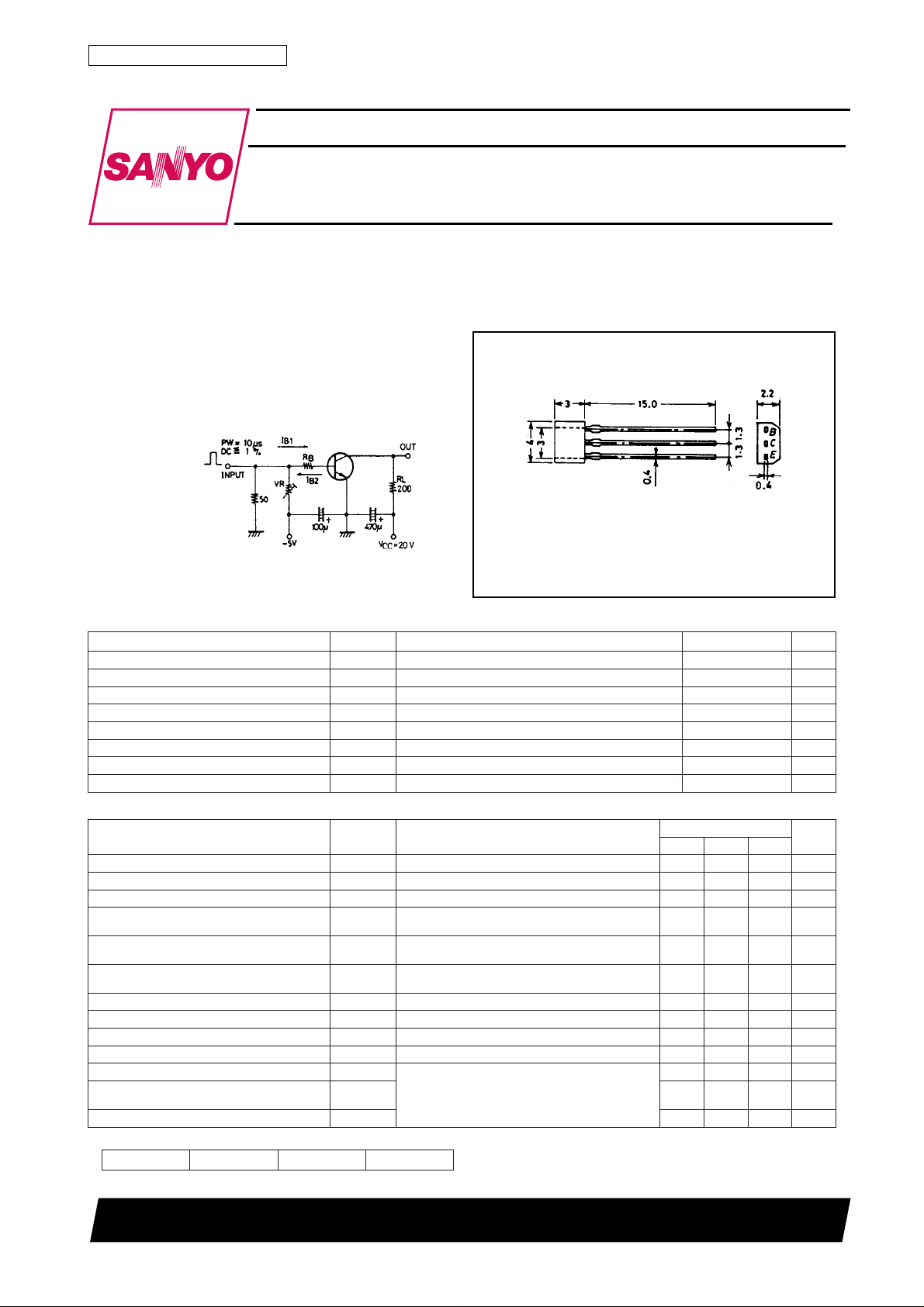
Package Dimensions
unit:mm
2033
· Complementary pair transistor having large current
capacity and high fT.
· Adoption of FBET process.
Switching Time T est Circuit
( ) : 2SA1339
(For PNP, the polarity is reversed)
Unit (resistance : Ω, capacitance : F)
Specifications
Absolute Maximum Ratings at Ta = 25˚C
retemaraPlobmySsnoitidnoCsgnitaRtinU
egatloVesaB-ot-rotcelloCV
egatloVrettimE-ot-rotcelloCV
egatloVesaB-ot-rettimEV
tnerruCrotcelloCI
)esluP(tnerruCrotcelloCI
noitapissiDrotcelloCP
erutarepmeTnoitcnuJjT 051
erutarepmeTegarotSgtsT 051+ot55–
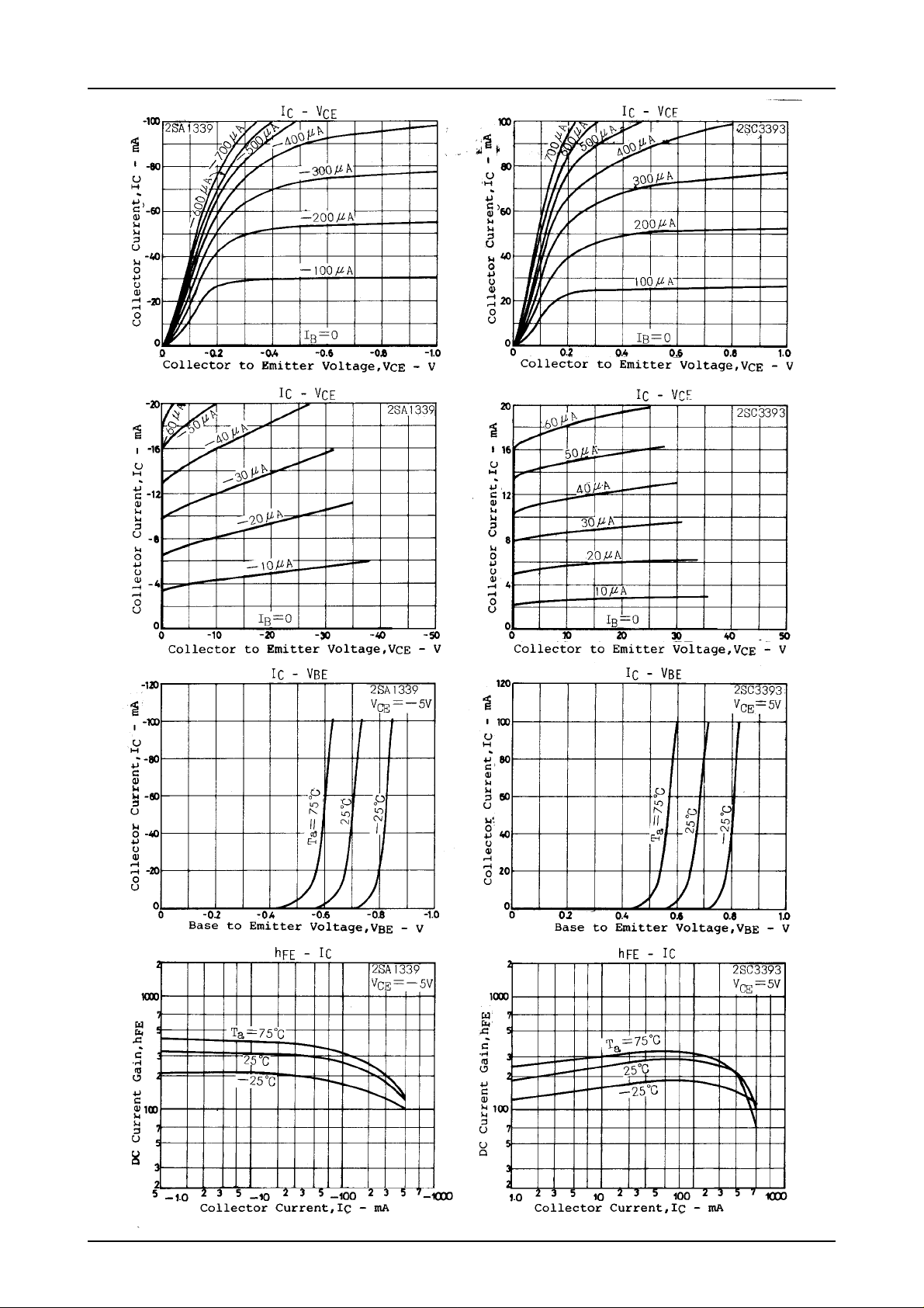
Electrical Characteristics at Ta = 25˚C
retemaraPlobmySsnoitidnoC
tnerruCffotuCrotcelloCI
tnerruCffotuCrettimEI
niaGtnerruCCD
tcudorPhtdiwdnaB-niaGf
ecnaticapaCtuptuOesaBnommoCC
egatloVnoitarutaSrettimE-ot-rotcelloCV
egatloVnoitarutaSrettimE-ot-esaBV
egatloVnwodkaerBesaB-ot-rotcelloCV
egatloVnwodkaerBrettimE-ot-rotcelloCV
egatloVnwodkaerBesaB-ot-rettimEV
emiTNO-nruTt
emiTegarotSt
emiTllaFt
* : The 2SA1339/2SC3393 are classified by 10mA hFE as follows :
002R001082T041004S002065U082
OBC
OEC
OBE
C
PC
C
V
OBC
OBE
h
EF
T
bo
no
gts
f
BC
V
BE
V
EC
V
EC
V
BC
I
)tas(EC
C
I
)tas(EB
C
I
OBC)RB(
C
I
OEC)RB(
C
I
OBE)RB(
E
V
CC
ICI01=
I,V04)–(=
0=1.0)–(Aµ
E
I,V4)–(=
0=1.0)–(Aµ
C
I,V5)–(=
C
I,Aµ01)–(=
E
I,Aµ01)–(=
C
V02=
1B
Am01)–(=*001*065
I,V01)–(=
C
I,Am001)–(=
I,Am001)–(=
R,Aµ001)–(=
I01–=
Am05)–(=003
zHM1=f,V01)–(=7.3
B
B
=∞ 5)–(V
Am01)–(=1.0
Am01)–(=8.02.1V
0=06)–(V
=∞ 05)–(V
EB
Am001=
2B
[2SA1339/2SC3393]
nimpytxam
B : Base
C : Collector
E : Emitter
SANYO : SPA
06)–(V
05)–(V
5)–(V
005)–(Am
008)–(Am
003Wm
sgnitaR
)002(
)6.5(
3.0
)51.0(
)4.0(
)07(07sn
004
)004(
)05(07sn
˚C
˚C
tinU
zHM
Fp
V
sn
SANYO Electric Co.,Ltd. Semiconductor Bussiness Headquaters
TOKYO OFFICE Tokyo Bldg., 1-10, 1 Chome, Ueno, Taito-ku, TOKYO, 110-8534 JAPAN
71598HA (KT)/3197KI/1114KI, MT No.1392-1/4
Page 2
2SA1339/2SC3393
No.1392-2/4
Page 3

2SA1339/2SC3393
No.1392-3/4
Page 4

2SA1339/2SC3393
No products described or contained herein are intended for use in surgical implants, life-support systems,
aerospace equipment, nuclear power control systems, vehicles, disaster/crime-prevention equipment and
the like, the failure of which may directly or indirectly cause injury, death or property loss.
Anyone purchasing any products described or contained herein for an above-mentioned use shall:
Accept full responsibility and indemnify and defend SANYO ELECTRIC CO., LTD., its affiliates,
subsidiaries and distributors and all their officers and employees, jointly and severally, against any
and all claims and litigation and all damages, cost and expenses associated with such use:
Not impose any responsibilty for any fault or negligence which may be cited in any such claim or
litigation on SANYO ELECTRIC CO., LTD., its affiliates, subsidiaries and distributors or any of
their officers and employees jointly or severally.
Information (including circuit diagrams and circuit parameters) herein is for example only; it is not guaranteed for volume production. SANYO believes information herein is accurate and reliable, but no guarantees
are made or implied regarding its use or any infringements of intellectual property rights or other rights of
third parties.
This catalog provides information as of July, 1998. Specifications and information herein are subject to
change without notice.
PS No.1392-4/4
 Loading...