

Page 1
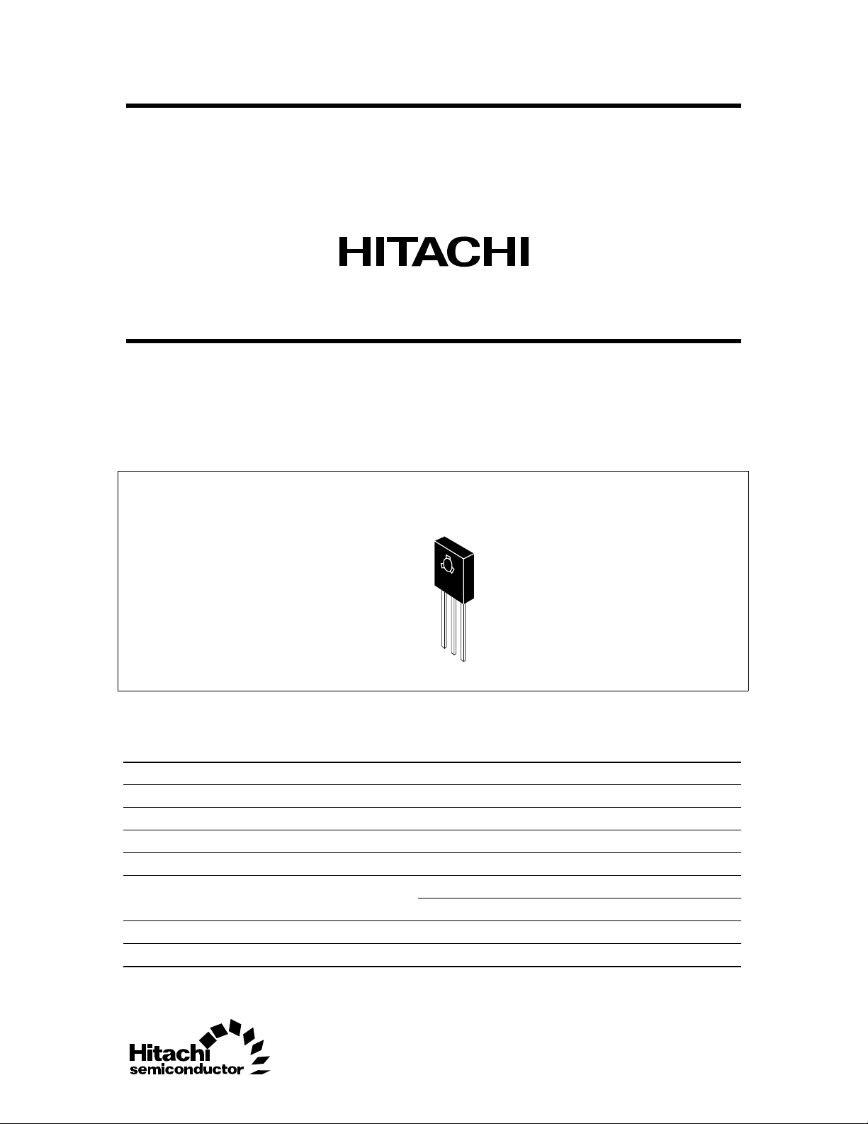
Silicon NPN Triple Diffused
Application
High speed and high voltage switching
Outline
TO-126 MOD
2SC2899
1. Emitter
2. Collector
1
2
3
3. Base
Absolute Maximum Ratings (Ta = 25°C)
Item Symbol Ratings Unit
Collector to base voltage V
Collector to emitter voltage V
Emitter to base voltage V
Collector current I
Collector peak current I
Collector power dissipation P
Junction temperature Tj 150 °C
Storage temperature Tstg –55 to +150 °C
Note: 1. Value at TC = 25°C.
CBO
CEO
EBO
C
C(peak)
C
PC*
1
500 V
400 V
10 V
0.5 A
1.0 A
0.75 W
10 W
Page 2
2SC2899
Electrical Characteristics (Ta = 25°C)
Item Symbol Min Typ Max Unit Test conditions
Collector to emitter sustain
voltage
Emitter to base breakdown
voltage
Collector cutoff current I
DC current transfer ratio h
Collector to emitter saturation
voltage
Base to emitter saturation
voltage
Turn on time t
Storage time t
Fall time t
Note: 1. Pulse test
V
CEO(sus)
V
CEX(sus)
V
(BR)EBO
CBO
I
CEO
FE1
h
FE2
V
CE(sat)
V
BE(sat)
on
stg
f
400 — — V IC = 0.1 A, RBE = , L = 100
mH
400 — — V IC = 0.5 A, IB1 = –IB2 = 0.1 A,
V
= –5 V, L = 180 µH,
BE
Clamped
10 — — V IE = 10 mA, IC = 0
— — 20 µA VCB = 400 V, IC = 0
— — 50 µA VCE = 350 V, RBE =
15 — — VCE = 5 V, IC = 0.25 A*
7—— V
= 5 V, IC = 0.5 A*
CE
— — 1.0 V IC = 0.25 A, IB = 0.05 A*
— — 1.5 V
— — 1.0 µs IC = 0.5 A, IB1 = –IB2 = 0.1 A,
— — 2.0 µs VCC ≅ 150 V
— — 1.0 µs
1
1
1
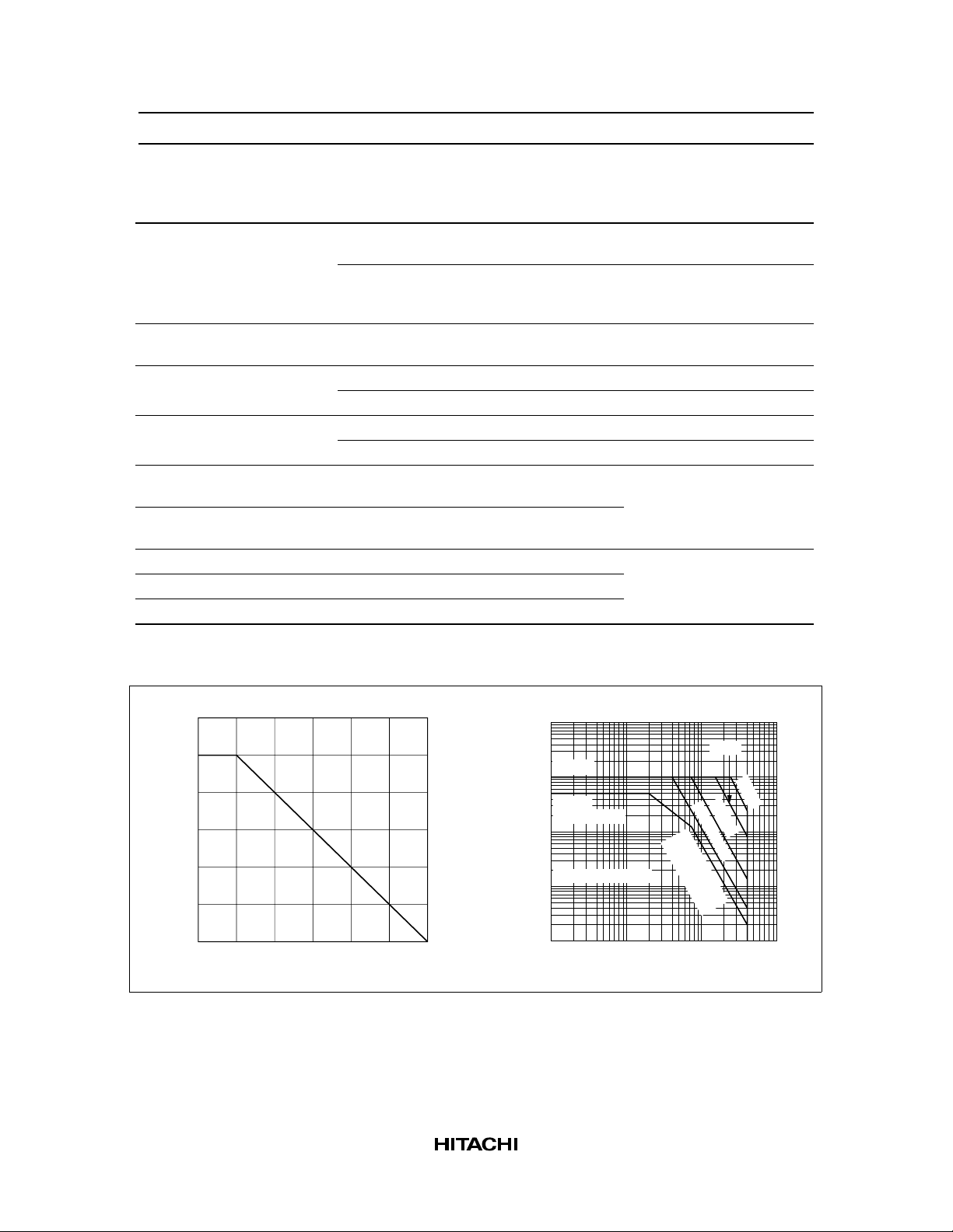
Maximum Collector Dissipation Curve
12
8
1
Collector power dissipation Pc (W)
0
50 100 150
Case Temperature T
C
(°C)
Area of Safe Operation
10
iC
(peak)
1.0
(A)
C
IC
(max)
(Continuous)
0.1
Ta = 25°C, 1 Shot
0.01
Collector Current I
PW = 1 ms
DC Operation
(T
C
= 25°C)
0.001
1 3 10 30 100 300 1,000
Collector to emitter Voltage VCE (V)
50 µs
25 µs
250 µs
2
Page 3
100
80
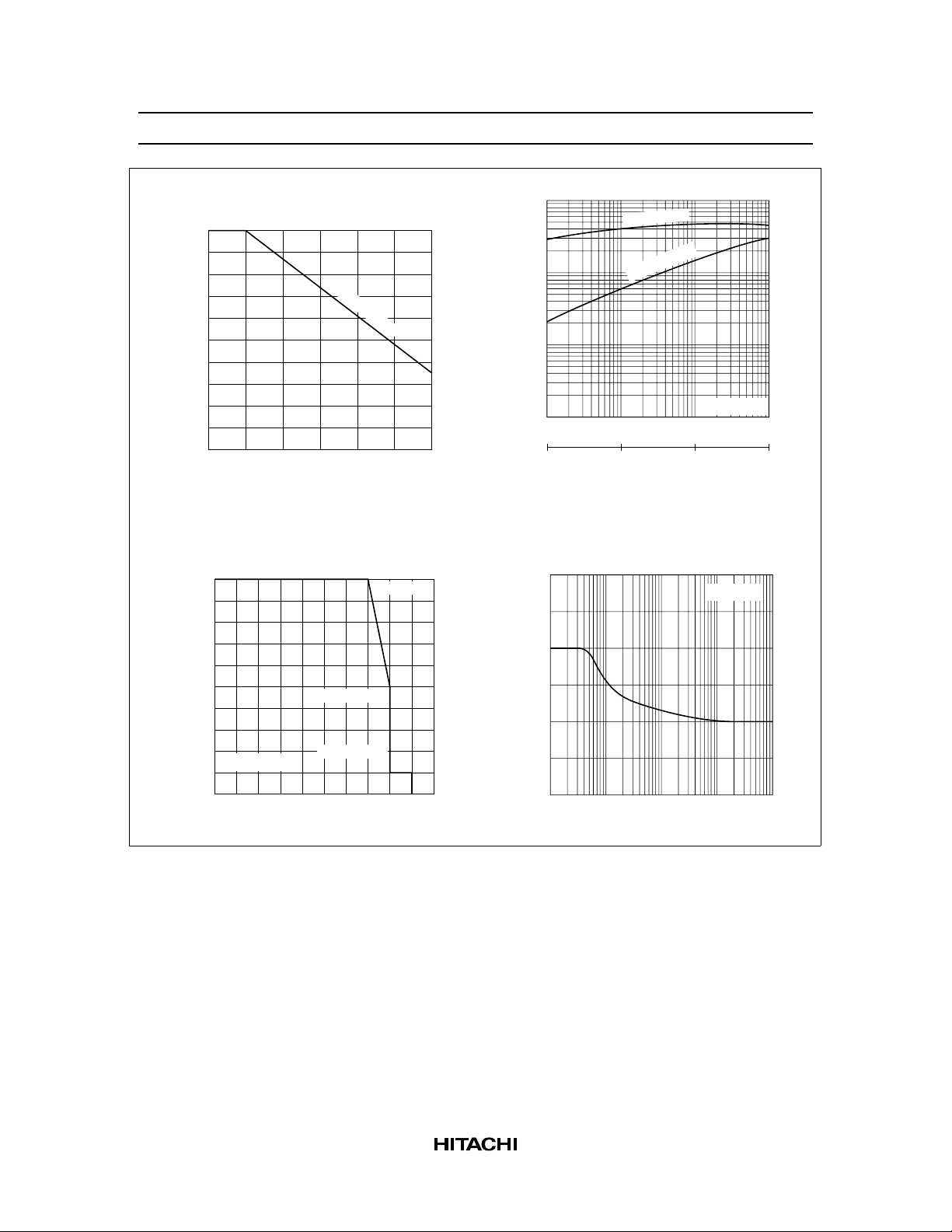
Collector Current Derating Rate
IS/B Limit Area
(°C/W)
j-c
10
1.0
2SC2899
Transient Thermal Resistance
10 ms–10 s
3
10 µs–10 ms
60
40
20
Collector Current derating rate (%)
0
50 100 150
Case temperature TC (°C)
Reverse Bias Area of Safe Operation
1.0
0.8
(A)
C
0.6
400 V, 0.5 A
0.4
Collector Current I
0.2
IB2 = –0.1 A
450 V, 0.1 A
0
0 100 200 300 400 500
Collector to emitter Voltage V
350 V, 1 A
(V)
CE
0.3
0.1
0.03
Thermal resistance θ
0.01
0.01 0.1 1.0 10 (s)
TC = 25°C
0.01 0.1 1.0 10 (ms)
Time t
Collector to Emitter Voltage
vs. Base to Emitter Resistance
600
(V)
CER
IC = 1 mA
500
400
Collector to emitter voltage V
300
100 1 k 10 k 100 k 1 M
Base to emitter resistance R
BE
(Ω)
3
Page 4
2SC2899
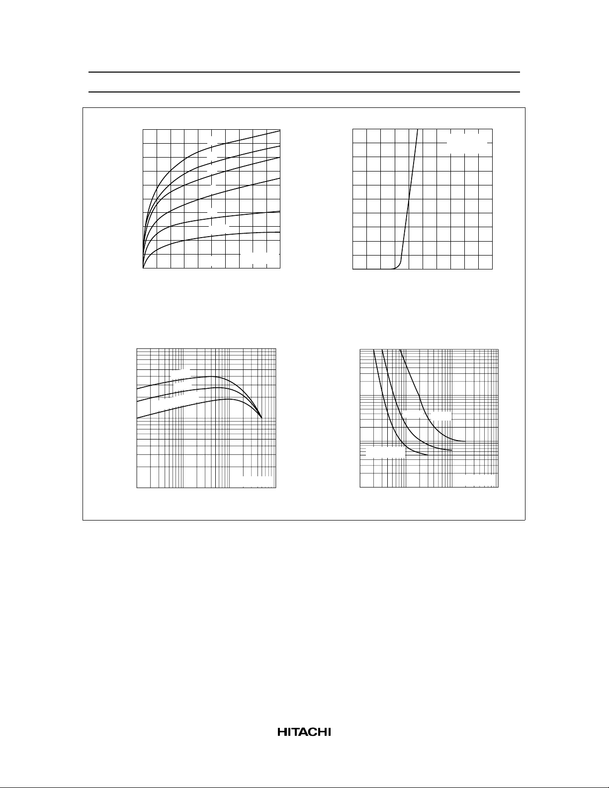
Typical Output Characteristics
0.5
50
0.4
(A)
C
0.3
0.2
40
30
20
10
5 mA
Collector Current I
0.1
IB = 0
0
12345
Collector to emitter Voltage V
DC Current Transfer Ratio vs.
Collector Current
100
FE
30
75°C
= –25°C
T
C
25°C
10
3
DC current transfer ratio h
1
0.001 0.003 0.01 0.03 0.1 0.3 1.0
Collector current I
TC = 25°C
V
CE
(A)
C
(V)
CE
= 5 V
Typical Transfer Characteristics
1.0
TC = 25°C
V
= 5 V
0.8
(A)
C
CE
0.6
0.4
Collector Current I
0.2
0
0.4 0.8 1.2 1.6 2.0
Base to emitter voltage V
BE
(V)
Collector to Emitter Saturation
Voltage vs. Base Current
10
3
1.0
(V)
0.1 A
0.3
CE (sat)
V
1.0
0.2 A
IC = 0.05 A
0.03
Collector to emitter saturation voltage
0.01
TC = 25°C
0.001 0.003 0.01 0.03 0.1 0.3 1.0
Base current I
B
(A)
4
Page 5
2SC2899
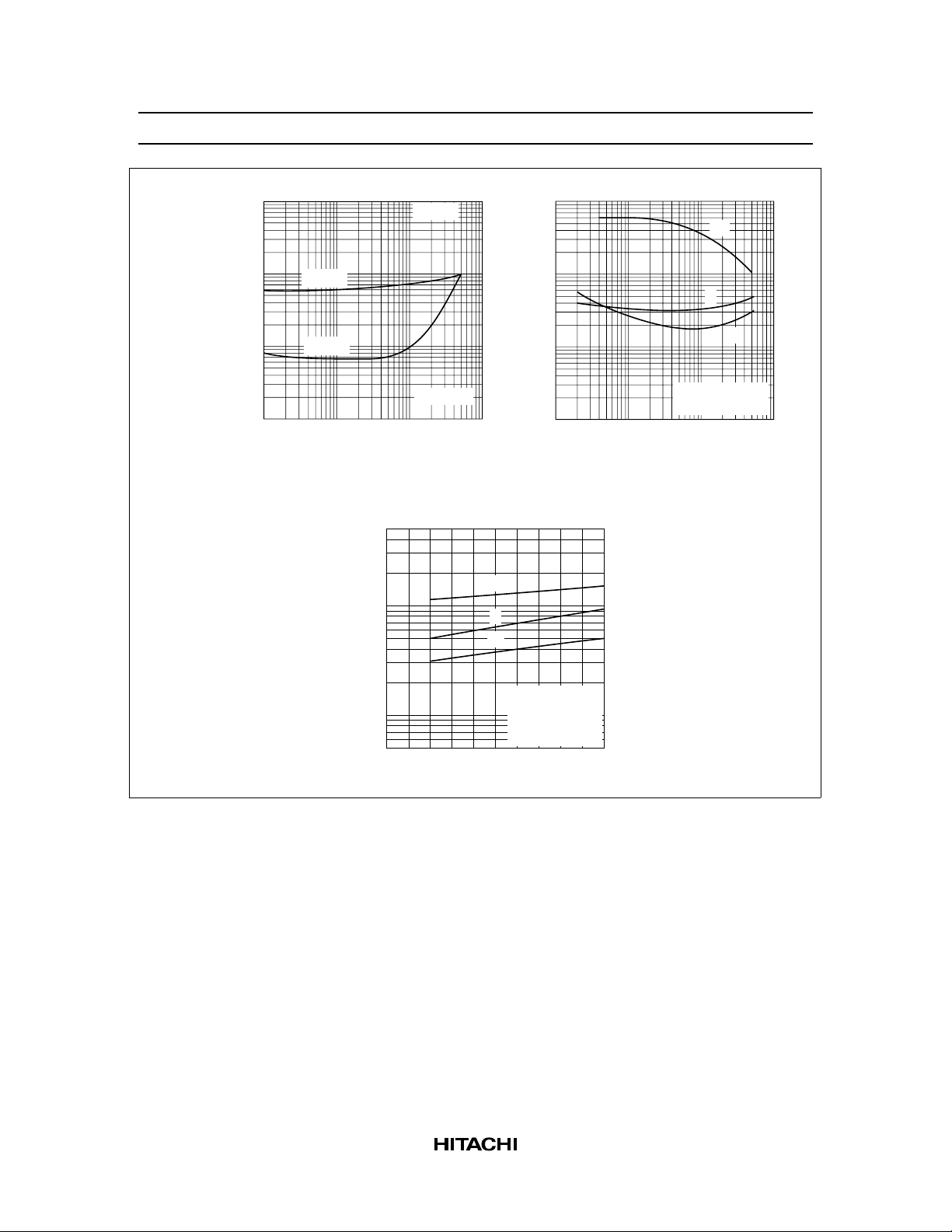
Saturation Voltage vs. Collector Current
10
3
(V)
1.0
(V)
V
BE (sat)
0.3
BE (sat)
CE (sat)
V
V
0.1
V
CE (sat)
0.03
Base to emitter saturation voltage
Collector to emitter saturation voltage
0.01
0.001 0.003 0.01 0.03 0.1 0.3 1.0
Collector current I
1.0
0.3
lC = 5 l
B
10
3
1.0
0.3
0.1
Switching time t (µs)
TC = 25°C
(A)
C
0.03
0.01
0.001 0.003 0.01 0.03 0.1 0.3 1.0
Switching Time vs. Case Temperature
5
3
t
stg
t
f
t
on
Switching Time vs. Collector Current
t
stg
t
f
t
on
IC = 5 I
VCC 150 V=
Collector current I
.
.
C
B1 =
(A)
–5 I
B2
Switching time t (µs)
0.1
0.05
0 25 50 75 100 125
IC = 0.5 A
I
B1 = –IB2
RL = 300 Ω
VCC 150 V
Case temperature T
.
=
.
(°C)
C
= 0.1 A
5
Page 6
2SC2899
When using this document, keep the following in mind:
1. This document may, wholly or partially, be subject to change without notice.
2. All rights are reserved: No one is permitted to reproduce or duplicate, in any form, the whole or part of
this document without Hitachi’s permission.
3. Hitachi will not be held responsible for any damage to the user that may result from accidents or any
other reasons during operation of the user’s unit according to this document.
4. Circuitry and other examples described herein are meant merely to indicate the characteristics and
performance of Hitachi’s semiconductor products. Hitachi assumes no responsibility for any intellectual
property claims or other problems that may result from applications based on the examples described
herein.
5. No license is granted by implication or otherwise under any patents or other rights of any third party or
Hitachi, Ltd.
6. MEDICAL APPLICATIONS: Hitachi’s products are not authorized for use in MEDICAL
APPLICATIONS without the written consent of the appropriate officer of Hitachi’s sales company.
Such use includes, but is not limited to, use in life support systems. Buyers of Hitachi’s products are
requested to notify the relevant Hitachi sales offices when planning to use the products in MEDICAL
APPLICATIONS.
Hitachi, Ltd.
Semiconductor & IC Div.
Nippon Bldg., 2-6-2, Ohte-machi, Chiyoda-ku, Tokyo 100, Japan
Tel: Tokyo (03) 3270-2111
Fax: (03) 3270-5109
For further information write to:
Hitachi America, Ltd.
Semiconductor & IC Div.
2000 Sierra Point Parkway
Brisbane, CA. 94005-1835
U S A
Tel: 415-589-8300
Fax: 415-583-4207
Hitachi Europe GmbH
Electronic Components Group
Continental Europe
Dornacher Straße 3
D-85622 Feldkirchen
München
Tel: 089-9 91 80-0
Fax: 089-9 29 30 00
6
Hitachi Europe Ltd.
Electronic Components Div.
Northern Europe Headquarters
Whitebrook Park
Lower Cookham Road
Maidenhead
Berkshire SL6 8YA
United Kingdom
Tel: 0628-585000
Fax: 0628-778322
Hitachi Asia Pte. Ltd.
16 Collyer Quay #20-00
Hitachi Tower
Singapore 0104
Tel: 535-2100
Fax: 535-1533
Hitachi Asia (Hong Kong) Ltd.
Unit 706, North Tower,
World Finance Centre,
Harbour City, Canton Road
Tsim Sha Tsui, Kowloon
Hong Kong
Tel: 27359218
Fax: 27306071
 Loading...