

Page 1
Transistor
2SC2636
Silicon NPN epitaxial planer type
For high-frequency amplification/oscillation
Features
■
●
High transition frequency fT.
●
M type package allowing easy automatic and manual insertion as
well as stand-alone fixing to the printed circuit board.
Absolute Maximum Ratings (Ta=25˚C)
■
Parameter
Collector to base voltage
Collector to emitter voltage
Emitter to base voltage
Collector current
Collector power dissipation
Junction temperature
Storage temperature
Electrical Characteristics (Ta=25˚C)
■
Parameter
Collector to base voltage
Emitter to base voltage
Forward current transfer ratio
Base to emitter voltage
Transition frequency
Power gain
Common base reverse transfer capacitance
Common emitter reverse transfer capacitance
Base time constant
Symbol
V
CBO
V
CEO
V
EBO
I
C
P
C
T
j
T
stg
Symbol
V
CBO
V
EBO
h
FE
V
BE
*
f
T
PG
C
rb
C
re
rbb' · C
Ratings
30
20
3
50
400
150
–55 ~ +150
IC = 100µA, IE = 0
IE = 10µA, IC = 0
VCB = 10V, IE = –2mA
VCB = 10V, IE = –2mA
VCB = 10V, IE = –15mA, f = 200MHz
VCB = 10V, IE = –1mA, f = 100MHz
VCB = 6V, IE = 0, f = 1MHz
VCE = 10V, IC = 1mA, f = 10.7MHz
VCB = 10V, IE = –10mA, f = 31.9MHz
C
Unit
V
V
V
mA
mW
˚C
˚C
Conditions
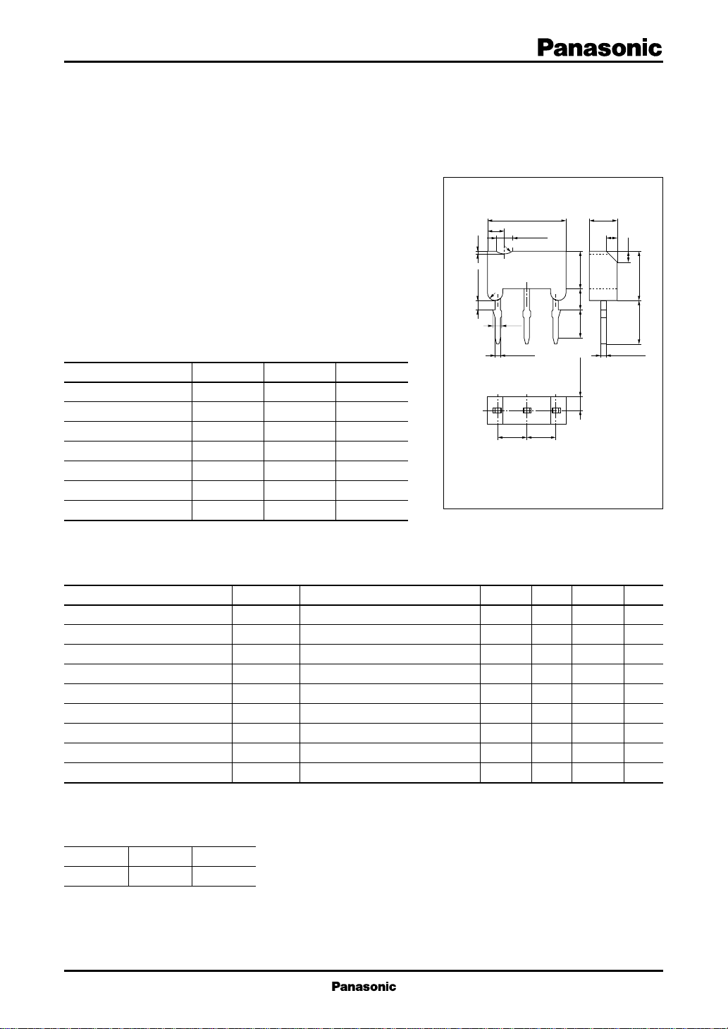
6.9±0.1
1.5
1.5 R0.9
0.4
R0.9
R0.7
1.0±0.1
0.85
0.55±0.1 0.45±0.05
2.5 2.5
1:Base
2:Collector EIAJ:SC–71
3:Emitter M Type Mold Package
min
typ
2.5±0.1
3.5±0.1
2.0±0.2
2.4±0.21.25±0.05
123
max
30
3
25
720
600
1200
1600
20
0.8
1.5
25
Unit: mm
1.0
1.0
4.1±0.2 4.5±0.1
Unit
V
V
mV
MHz
dB
pF
pF
ps
*
fT Rank classification
Rank T S
f
600 ~ 1300 900 ~ 1600
T
1
Page 2
Transistor
2SC2636
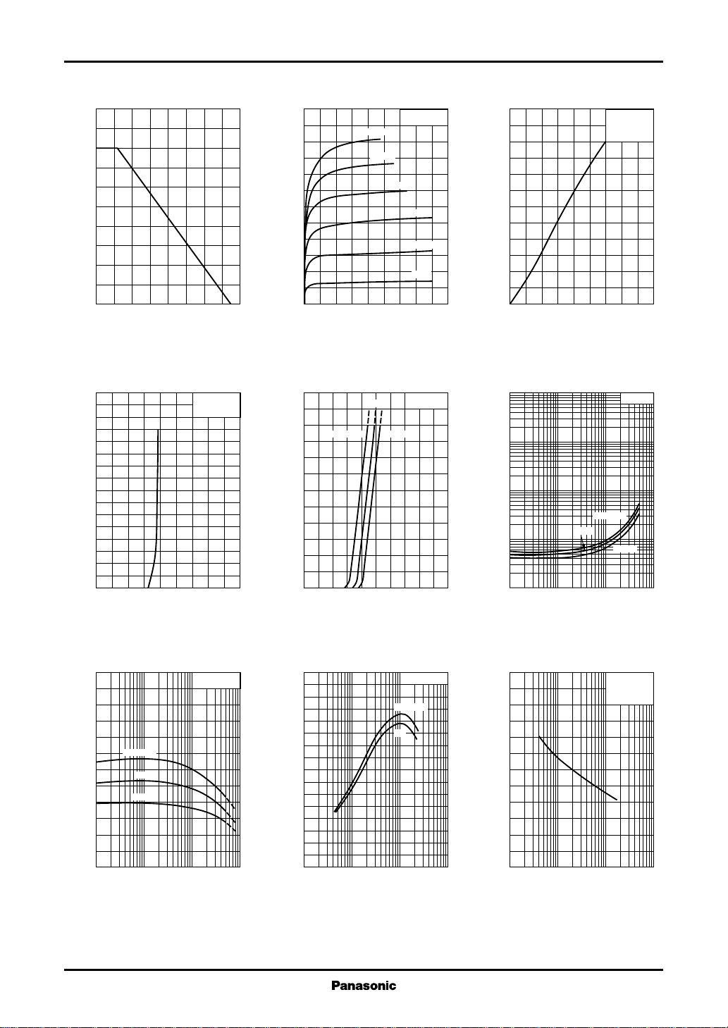
PC — Ta IC — V
500
)
mW
(
400
C
300
200
100
Collector power dissipation P
0
0 16040 12080 14020 10060
Ambient temperature Ta (˚C
IB — V
BE
400
350
300
)
µA
(
250
B
200
VCE=10V
Ta=25˚C
CE
24
20
)
mA
(
16
C
12
8
Collector current I
4
0
018612
)
Collector to emitter voltage VCE (V
IB=300µA
IC — V
60
50
)
mA
(
C
Ta=75˚C
40
30
250µA
25˚C
Ta=25˚C
200µA
150µA
100µA
50µA
)
BE
VCE=10V
–25˚C
24
20
)
mA
(
16
C
12
8
Collector current I
4
0
0 450150 300
)
100
V
(
30
CE(sat)
10
3
1
IC — I
B
VCE=10V
Ta=25˚C
Base current IB (µA
V
— I
CE(sat)
C
)
IC/IB=10
150
Base current I
100
50
0
01.80.6 1.2
Base to emitter voltage VBE (V
hFE — I
C
240
FE
200
160
Ta=75˚C
120
80
40
Forward current transfer ratio h
0
0.1 1 10 1000.3 3 30
25˚C
–25˚C
VCE=10V
Collector current IC (mA
20
Collector current I
10
0
0 2.01.60.4 1.20.8
)
)
Base to emitter voltage VBE (V
fT — I
E
1600
1400
)
MHz
1200
(
T
1000
800
600
400
Transition frequency f
200
0
0.1 1 10 1000.3 3 30
Emitter current IE (mA
VCE=10V
6V
)
Ta=25˚C
)
0.3
0.1
0.03
0.01
Collector to emitter saturation voltage V
0.1 1 10 1000.3 3 30
Collector current IC (mA
Cre — V
)
2.4
pF
(
re
2.0
1.6
1.2
0.8
0.4
Common emitter reverse transfer capacitance C
0
0.1 1 10 1000.3 3 30
Collector to emitter voltage VCE (V
25˚C
Ta=75˚C
CE
–25˚C
)
IC=1mA
f=10.7MHz
Ta=25˚C
)
2
Page 3

Transistor
2SC2636
Zrb — I
E
120
)
Ω
(
100
rb
80
60
40
20
VCE=6V
Reverse transfer impedance Z
0
– 0.1 – 0.3 –1 –3 –10
Emitter current IE (mA
bib — g
ib
0
–10
)
mS
(
–20
IE=–2mA
ib
f=900MHz
–5mA
–30
–40
Input susceptance b
–50
–60
0504010 3020
600
500
yib=gib+jb
VCB=10V
Input conductance gib (mS
f=2MHz
Ta=25˚C
10V
)
300
200
PG — I
E
40
35
)
30
dB
(
25
20
15
Power gain PG
10
5
0
– 0.1 –1 –10 –100– 0.3 –3 –30
Emitter current IE (mA
brb — g
0
)
ib
)
yrb=grb+jb
rb
VCB=10V
mS
(
– 0.4
rb
– 0.8
–1.2
–1.6
–2.0
Reverse transfer susceptance b
–2.4
–1.0 0– 0.2– 0.8 – 0.4– 0.6
Reverse transfer conductance grb (mS
VCE=10V
rb
f=900MHz
IE=–5mA
f=100MHz
R
=50Ω
g
Ta=25˚C
6V
)
200
300
500
600
–2mA
12
10
)
dB
(
8
6
4
Noise figure NF
2
0
– 0.1 –1 –10 –100– 0.3 –3 –30
48
)
mS
(
40
fb
32
24
16
8
Forward transfer susceptance b
0
–60 4020–40 0–20
)
Forward transfer conductance gfb (mS
NF — I
E
VCE=10V
f=100MHz
R
=50kΩ
g
Ta=25˚C
Emitter current IE (mA
bfb — g
fb
yfb=gfb+jb
VCB=10V
f=200MHz
IE=–5mA
–2mA
300
900
)
fb
500
600
)
bob — g
12
yob=gob+jb
ob
VCE=10V
)
10
mS
(
ob
8
IE=–2mA –5mA
6
4
2
Output susceptance b
0
02.01.60.4 1.20.8
Output conductance gob (mS
500
300
f=200MHz
ob
900
600
)
3
 Loading...