

Page 1
High voltage discharge, High speed switching,
Low Noise (−60V, −3A)
2SA2072
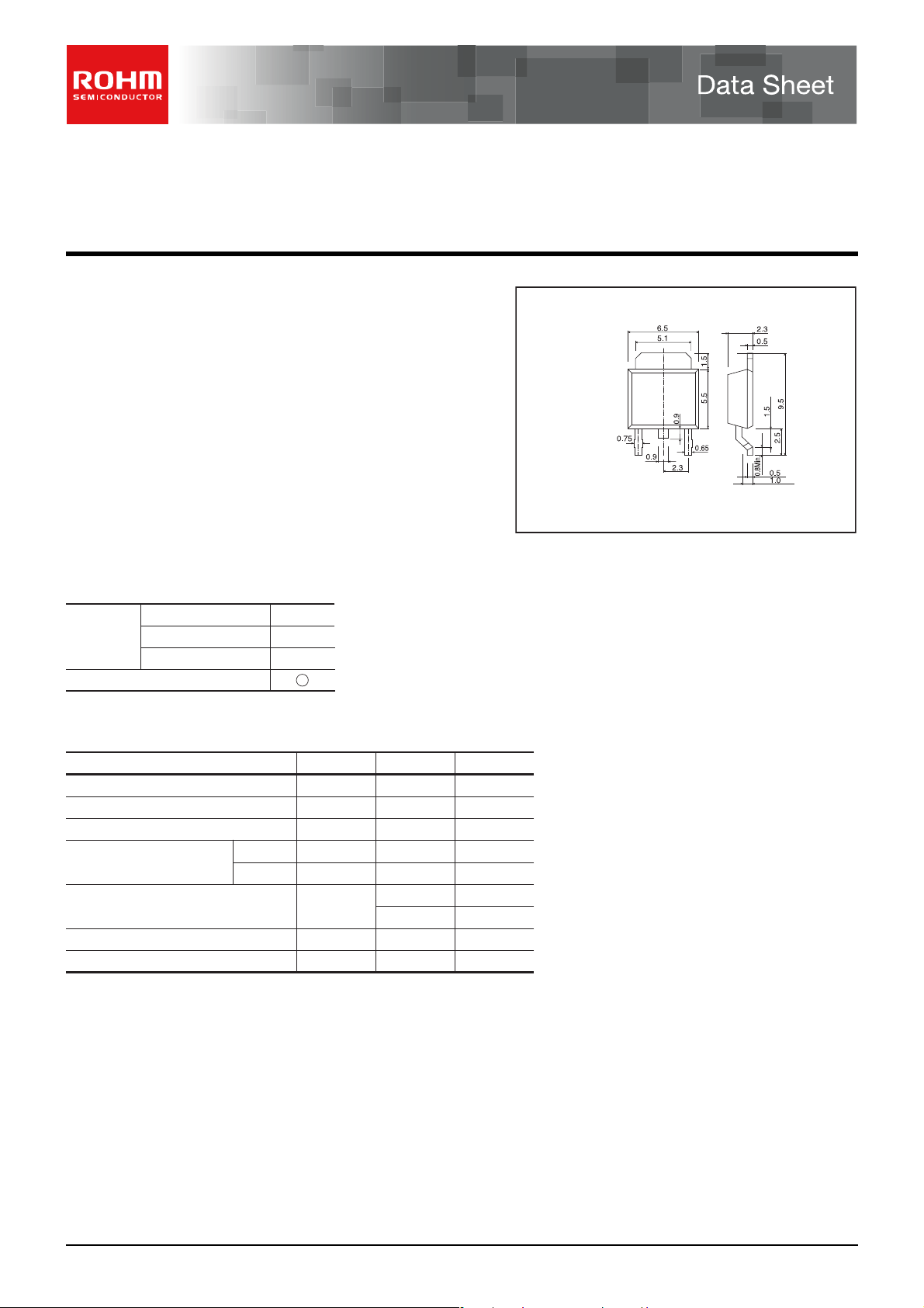
zFeatures zDimensions (Unit : mm)
−
CBO
CEO
EBO
I
C
CP
tj
3A)
=
CPT3
(SC-63)
<SOT-428>
(1) Base
(2) Collector
(3) Emitter
Abbreviated symbol : A2072
Limits Unit
−60
−60
−6
−3
∗1
C
−6
1.0
10.0
150
−55 to 150
∗2
∗3
V
V
V
A
A
W
W
°C
°C
1) High speed switching. ( tf : Typ. : 20ns
at IC
2) Low saturation voltage, typically.
(Typ. : −200mV at IC =
−
2.0A, I
B
=
−
200mA)
3) Strong discharge power for inductive load and capacitance load.
4) Low Noise.
5) Complements the 2SC5825.
zApplications
High speed switching, Low noise
zStructure
PNP silicon epitaxial planar transistor
zPackaging specifications
Taping
TL
2500
Type
2SA2072
Package
Code
Basic ordering unit (pieces)
zAbsolute maximum ratings (Ta=25°C)
Parameter
Collector-base voltage
Collector-emitter voltage
Emitter-base voltage
Collector current
Power dissipation
Junction temperature
Range of storage temperature
∗1 Pw=100ms
∗2 Ta=25°C
∗3 Tc=25°C
DC
Pulsed
Symbol
V
V
V
I
P
tstg
www.rohm.com
c
○
2009 ROHM Co., Ltd. All rights reserved.
1/3
2009.02 - Rev.B
Page 2
V)
s
.5
)
n
0
1000
DC CURRENT GAIN : h
0
1000
DC CURRENT GAIN : h
)
0
1
)
e
0
1
)
e
2SA2072
zElectrical characteristics (Ta=25°C)
Parameter Symbol Min. Typ. Max. Unit Condition
BV
Collector-emitter breakdown voltage
Collector-base breakdown voltage
Emitter-base breakdown voltage
Collector cut-off current
Emitter cut-off current
Collector-emitter saturation voltage
DC current gain
Transistor frequency
Collector output capacitance
Turn-on time
Storage time
Fall time
∗1 Non repetitive pulse
∗2 See switching characteristics measurement circuits
zhFE RANK
Q
120−270
zElectrical characteristics curves
200
160
(mA)
C
120
80
40
COLLECTOR CURRENT : I
0
COLLECTOR TO EMITTER VOLTAGE : V
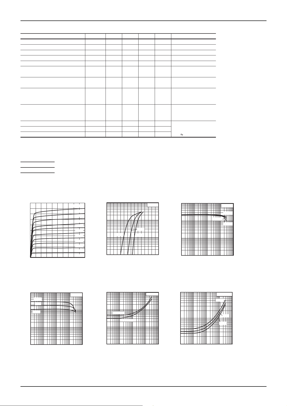
Fig.1 Typical output characteristic
125°C
FE
25°C
100
−40°C
10
IB=1000µA
900µA
800µA
700µA
600µA
500µA
400µA
300µA
200µA
100µA
0µA
Ta=25°C
512340
CE
(
CEO
BV
CBO
BV
EBO
I
CBO
I
EBO
∗1
V
CE (sat)
h
FE
∗1
f
T
Cob
∗2
ton
∗2
tstg
∗2
tf
(A)
C
COLLECTOR CURRENT : I
0.01
(V
CE(sat)
0.01
−60
−60
−6
−
−
−
120
−
−
−
−
−
10
1
0.1
0 0.1 0.2 0.3 0.4 0.50.6 0.7 0.80.9 1 1.1 1.2 1.31.4 1
BASE TO EMITTER VOLTAGE : VBE (V
−
−
−
−
−
−200
−
180
50
20
150
20
125°C
Fig.2 Grounded emitter propagatio
characteristics
0.1
Ic/Ib=20/1
Ic/Ib=10/1
25°C
−40°C
−
−
−
−1.0
−1.0
−500
270
−
−
−
−
−
VCE=2V
Ta=25
°C
V
V
V
µA
µA
mV
−
MHz
pF
ns
ns
ns
C
=
−1mA
I
C
=
−100µA
I
I
E
= −100µA
V
CB
= −20V
EB
= −4V
V
I
C
= −2A
I
B
= −0.2A
V
CE
= −2V
C
= −100mA
I
CE
= −10V
V
E
=100mA
I
=10MHz
f
CB
= −10V
V
E
=0mA
I
=1MHz
f
C
= −3A
I
B1
= −300mA
I
B2
=300mA
I
CC
−25V
V
FE
100
10
1
0.001 0.01 0.1 1
COLLECTOR CURRENT : I
Fig.3 DC current gain
vs.collector current ( Ι )
(V
CE(sat)
0.1
VCE=3V
IC/Ib
125°C
Ta=25
1
C
−40°C
Data Sheet
°C
VCE=5V
VCE=2V
(A)
=10/1
25°C
1
0.001 0.01 0.1 1
www.rohm.com
c
○
2009 ROHM Co., Ltd. All rights reserved.
1
C
COLLECTOR CURRENT : I
(A)
Fig.4 DC current gain
vs.collector current ( ΙΙ
0.001
0.001 0.01 0.1 1
COLLECTOR SATURATION VOLTAGE : V
COLLECTOR CURRENT : I
1
C
(A)
Fig.5 Collector-emitter saturation voltag
vs.collector current ( Ι )
2/3
0.01
0.001 0.01 0.1 1
COLLECTOR SATURATION VOLTAGE : V
COLLECTOR CURRENT : IC (A)
1
Fig.6 Collector-emitter saturation voltag
vs.collector current ( ΙΙ )
2009.02 - Rev.B
Page 3
0
)
e
0
1000
TRANSITION FREQUENCY : f
(MHz)
0
1000
V)
e
0
V
B
W
C
W
2SA2072
(V
BE(sat)
10
1
−40°C
IC/Ib
=10/1
Ta=25
°C
CE
=10V
V
T
100
(pF)
100
Ta=25°C
f=1MHz
Data Sheet
25°C
125°C
0.1
0.001 0.01 0.1 1
BASE EMITTER SATURATION VOLTAGE : V
COLLECTOR CURRENT : IC (A)
1
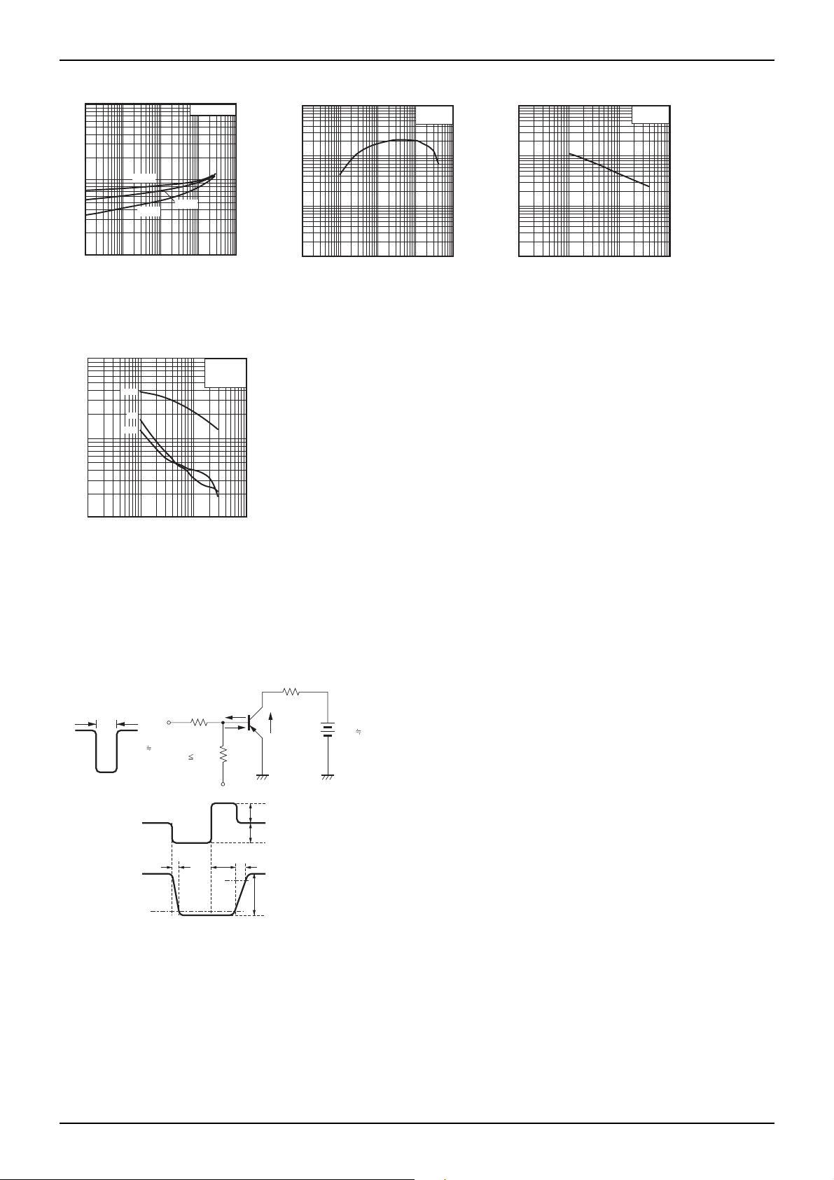
Fig.7 Base-emitter saturation voltag
10
1
0.001 0.01 0.1 1
EMITTER CURRENT : I
Fig.8 Transition frequency
vs. collector current
1000
100
SW (ns)
tstg
tf
ton
10
COLLECTOR CURRENT : IC (A)
Fig.10 Switching Time
10.10.01
Ta=25°C
V
CC
=25V
C/IB
=10/1
I
1
zSwitching characteristics measurement circuits
RL=8.3Ω
C
I
P
V
IN
W
PW 50µs
DUTY CYCLE 1%
B1
I
B2
I
VCC −25
10
1
1
E
(A)
COLLECTOR OUTPUT CAPACITANCE : Cob
0.1 10 10
COLLECTOR TO BASE VOLTAGE : V
1
CB (
Fig.9 Collector output capacitanc
ASE CURRENT
AVEFORM
OLLECTOR CURRENT
AVEFORM
www.rohm.com
c
○
2009 ROHM Co., Ltd. All rights reserved.
90%
ton tstg tf
10%
I
B2
I
B1
C
I
3/3
2009.02 - Rev.B
Page 4

Appendix
No copying or reproduction of this document, in part or in whole, is permitted without the consent of ROHM
Co.,Ltd.
The content specified herein is subject to change for improvement without notice.
The content specified herein is for the purpose of introducing ROHM's products (hereinafter "Products"). If you
wish to use any such Product, please be sure to refer to the specifications, which can be obtained from ROHM
upon request.
Examples of application circuits, circuit constants and any other information contained herein illustrate the
standard usage and operations of the Products. The peripheral conditions must be taken into account
when designing circuits for mass production.
Great care was taken in ensuring the accuracy of the information specified in this document. However, should
you incur any damage arising from any inaccuracy or misprint of such information, ROHM shall bear no re-
sponsibility for such damage.
The technical information specified herein is intended only to show the typical functions of and examples
of application circuits for the Products. ROHM does not grant you, explicitly or implicitly, any license to
use or exercise intellectual property or other rights held by ROHM and other parties. ROHM shall bear no re-
sponsibility whatsoever for any dispute arising from the use of such technical information.
The Products specified in this document are intended to be used with general-use electronic equipment
or devices (such as audio visual equipment, office-automation equipment, communication devices, elec-
tronic appliances and amusement devices).
The Products are not designed to be radiation tolerant.
While ROHM always makes efforts to enhance the quality and reliability of its Products, a Product may fail or
malfunction for a variety of reasons.
Please be sure to implement in your equipment using the Products safety measures to guard against the
possibility of physical injury, fire or any other damage caused in the event of the failure of any Product, such as
derating, redundancy, fire control and fail-safe designs. ROHM shall bear no responsibility whatsoever for your
use of any Product outside of the prescribed scope or not in accordance with the instruction manual.
The Products are not designed or manufactured to be used with any equipment, device or system
which requires an extremely high level of reliability the failure or malfunction of which may result in a direct
threat to human life or create a risk of human injury (such as a medical instrument, transportation equipment,
aerospace machinery, nuclear-reactor controller, fuel-controller or other safety device). ROHM shall bear
no responsibility in any way for use of any of the Products for the above special purposes. If a Product is intend-
ed to be used for any such special purpose, please contact a ROHM sales representative before purchasing.
If you intend to export or ship overseas any Product or technology specified herein that may be controlled under
the Foreign Exchange and the Foreign Trade Law, you will be required to obtain a license or permit under the Law.
Notes
Thank you for your accessing to ROHM product informations.
More detail product informations and catalogs are available, please contact your nearest sales office.
ROHM Customer Support System
www.rohm.com
Copyright © 2009 ROHM Co.,Ltd.
21 Saiin Mizosaki-cho, Ukyo-ku, Kyoto 615-8585, Japan
THE AMERICAS / EUROPE / ASIA / JAPAN
Contact us : webmaster@ rohm.co. jp
TEL : +81-75-311-2121
FAX : +81-75-315-0172
Appendix-Rev4.1
 Loading...