

Page 1
查询2SA0777供应商
Transistors
2SA0777 (2SA777)
Silicon PNP epitaxial planar type
For low-frequency driver amplification
Complementary to 2SC1509
■ Features
• High collector-emitter voltage (Base open) V
• Optimum for the driver stage of a low-frequency and 25 W to 30 W
output amplifier.
CEO
■ Absolute Maximum Ratings Ta = 25°C
0.7
±0.1
5.9
±0.2
+0.3
±0.2
8.6
–0.2
0.7
±0.5
13.5
4.9
Unit: mm
±0.2
Parameter Symbol Rating Unit
Collector-base voltage (Emitter open) V
Collector-emitter voltage (Base open) V
Emitter-base voltage (Collector open) V
Collector current I
Peak collector current I
Collector power dissipation P
Junction temperature T
Storage temperature T
CBO
CEO
EBO
C
CP
C
j
−55 to +150 °C
stg
−80 V
−80 V
−5V
− 0.5 A
−1A
1W
150 °C
0.45
+0.2
–0.1
132
(1.27)(1.27)
2.54
+0.2
0.45
–0.1
(3.2)
±0.15
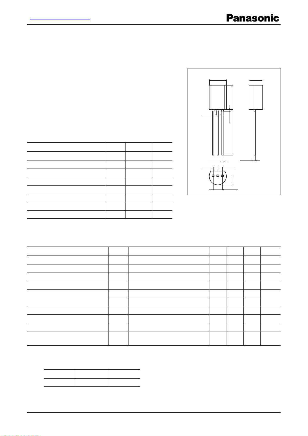
TO-92L-A1 Package
1 : Emitter
2 : Collector
3 : Base
EIAJ : SC-51
■ Electrical Characteristics Ta = 25°C ± 3°C
Parameter Symbol Conditions Min Typ Max Unit
Collector-base voltage (Emitter open) V
Collector-emitter voltage (Base open) V
Emitter-base voltage (Collector open) V
Collector-base cutoff current (Emitter open)
1
Forward current transfer ratio
*
Collector-emitter saturation voltage V
Base-emitter saturation voltage V
Transition frequency f
Collector output capacitance C
CBOIC
CEOIC
EBOIE
I
CBO
h
FE1
h
FE2
CE(sat)IC
BE(sat)IC
T
ob
(Common base, input open circuited)
Note) 1. Measuring methods are based on JAPANESE INDUSTRIAL STANDARD JIS C 7030 measuring methods for transistors.
2.*1: Palse measurement
2: Rank classification
*
Rank Q R
h
FE1
90 to 155 130 to 220
= −10 µA, IE = 0 −80 V
= −100 µA, IB = 0 −80 V
= −1 µA, IC = 0 −5V
VCB = −20 V, IE = 0 − 0.1 µA
2
*
VCE = −10 V, IC = −150 mA 90 220
VCE = −5 V, IC = −500 mA 50 100
= −500 mA, IB = −50 mA − 0.2 − 0.4 V
= −500 mA, IB = −50 mA − 0.85 −1.2 V
VCB = −10 V, IE = 50 mA, f = 200 MHz 120 MHz
VCB = −10 V, IE = 0, f = 1 MHz 11 20 pF
Note) The part number in the parenthesis shows conventional part number.
Publication date: November 2002 SJC00004BED
1
Page 2
2SA0777
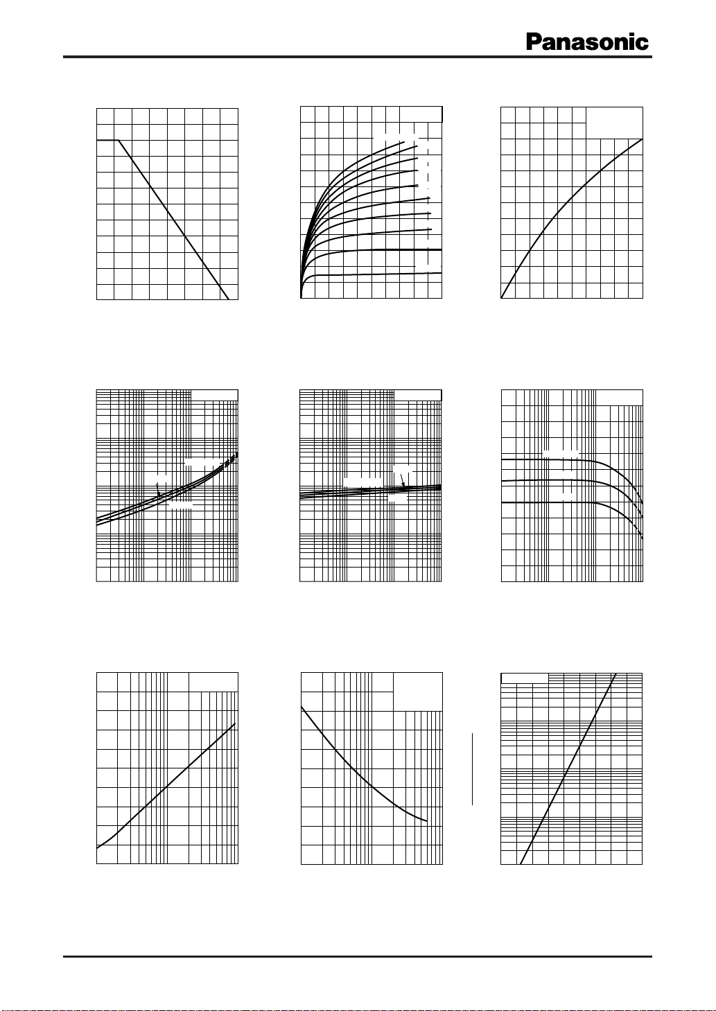
PC T
1.2
)
1.0
W
(
C
0.8
0.6
0.4
0.2
Collector power dissipation P
0
0 16040 12080 14020 10060
a
Ambient temperature Ta (°C
V
I
−10
)
V
(
CE(sat)
−1
− 0.1
− 0.01
Collector-emitter saturation voltage V
− 0.001
−1 −10 −100
CE(sat)
25°C
C
IC / IB = 10
Ta = 75°C
−25°C
Collector current IC (mA
IC V
BE(sat)
Ta = −25°C
CE
IB = −10 mA
I
C
IC / IB = 10
25°C
75°C
Ta = 25°C
−9 mA
−8 mA
−7 mA
−6 mA
−5 mA
−4 mA
−3 mA
−2 mA
−1 mA
−1.2
−1.0
)
A
(
− 0.8
C
− 0.6
− 0.4
Collector current I
− 0.2
0
0 −10−8−2 −6−4
)
300
250
FE
200
150
100
Forward current transfer ratio h
50
−1.2
−1.0
)
A
(
− 0.8
C
− 0.6
− 0.4
Collector current I
− 0.2
0
0 −10−8−2 −6−4
)
Collector-emitter voltage VCE (V
V
−100
)
V
(
BE(sat)
−10
−1
− 0.1
IC I
B
VCE = −10 V
= 25°C
T
a
Base current IB (mA
hFE I
C
VCE = −10 V
Ta = 75°C
25°C
−25°C
)
Base-emitter saturation voltage V
−1 000
)
− 0.01
−1 −10 −100
Collector current IC (mA
−1 000
)
0
−1 −10 −100
Collector current IC (mA
−1 000
)
fT I
200
180
)
160
MHz
(
140
T
120
100
80
60
40
Transition frequency f
20
0
1 10 100
Emitter current IE (mA
2
E
VCB = −10 V
= 25°C
T
a
(pF)
ob
C
Cob V
50
40
CB
IE = 0
f = 1 MHz
= 25°C
T
a
4
10
3
10
VCB = −20 V
I
CBO
T
a
)
30
20
10
Collector output capacitance
(Common base, input open circuited)
0
−1 −10 −100
)
Collector-base voltage VCB (V
)
a
T
(
= 25°C
2
a
10
T
(
CBO
I
CBO
I
10
1
)
0 18060 12040 100 16014020 80
Ambient temperature Ta (°C
)
SJC00004BED
Page 3
2SA0777
I
T
5
10
4
10
CEO
VCE = −10 V
)
3
10
)
a
T
(
= 25°C
a
T
(
CEO
I
2
10
CEO
I
a
)
A
(
Collector current I
10
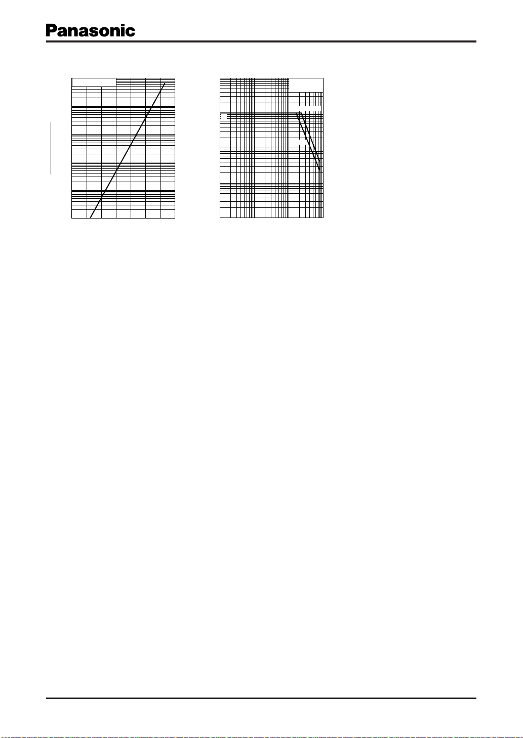
Safe operation area
−10
I
CP
−1
I
C
C
− 0.1
− 0.01
Single pulse
= 25°C
T
a
t = 10 ms
t = 1 s
1
0 1406020 80 12040 100
Ambient temperature Ta (°C
− 0.001
− 0.1 −1 −10 −100
)
Collector-emitter voltage VCE (V
)
SJC00004BED
3
Page 4

Request for your special attention and precautions in using the technical information
and semiconductors described in this material
(1) An export permit needs to be obtained from the competent authorities of the Japanese Government
if any of the products or technologies described in this material and controlled under the "Foreign
Exchange and Foreign Trade Law" is to be exported or taken out of Japan.
(2) The technical information described in this material is limited to showing representative characteris-
tics and applied circuits examples of the products. It neither warrants non-infringement of intellectual property right or any other rights owned by our company or a third party, nor grants any license.
(3) We are not liable for the infringement of rights owned by a third party arising out of the use of the
product or technologies as described in this material.
(4) The products described in this material are intended to be used for standard applications or general
electronic equipment (such as office equipment, communications equipment, measuring instruments and household appliances).
Consult our sales staff in advance for information on the following applications:
• Special applications (such as for airplanes, aerospace, automobiles, traffic control equipment,
combustion equipment, life support systems and safety devices) in which exceptional quality and
reliability are required, or if the failure or malfunction of the products may directly jeopardize life or
harm the human body.
• Any applications other than the standard applications intended.
(5) The products and product specifications described in this material are subject to change without
notice for modification and/or improvement. At the final stage of your design, purchasing, or use of
the products, therefore, ask for the most up-to-date Product Standards in advance to make sure that
the latest specifications satisfy your requirements.
(6) When designing your equipment, comply with the guaranteed values, in particular those of maxi-
mum rating, the range of operating power supply voltage, and heat radiation characteristics. Otherwise, we will not be liable for any defect which may arise later in your equipment.
Even when the products are used within the guaranteed values, take into the consideration of
incidence of break down and failure mode, possible to occur to semiconductor products. Measures
on the systems such as redundant design, arresting the spread of fire or preventing glitch are
recommended in order to prevent physical injury, fire, social damages, for example, by using the
products.
(7) When using products for which damp-proof packing is required, observe the conditions (including
shelf life and amount of time let standing of unsealed items) agreed upon when specification sheets
are individually exchanged.
(8) This material may be not reprinted or reproduced whether wholly or partially, without the prior written
permission of Matsushita Electric Industrial Co., Ltd.
2002 JUL
 Loading...