

Page 1
Ordering Information
2N7007
N-Channel Enhancement-Mode
Vertical DMOS FET
BV
/R
DSS
BV
DGS
240V 45Ω 150mA 2N7007
DS(ON)
(max) (min) TO-92
I
D(ON)
Order Number / Package
Features
■■ Free from secondary breakdown
■■ Low power drive requirement
■■ Ease of paralleling
■■ Low C
■■ Excellent thermal stability
■■ Integral Source-Drain diode
■■ High input impedance and high gain
■■ Complementary N- and P-channel devices
and fast switching speeds
ISS
Applications
■■ Motor controls
■■ Converters
■■ Amplifiers
■■ Switches
■■ Power supply circuits
■■ Drivers (relays, hammers, solenoids, lamps,
memories, displays, bipolar transistors, etc.)
Advanced DMOS Technology
These enhancement-mode (normally-off) transistors utilize a
vertical DMOS structure and Supertex’s well-proven silicon-gate
manufacturing process. This combination produces devices with
the power handling capabilities of bipolar transistors and with the
high input impedance and positive temperature coefficient inherent in MOS devices. Characteristic of all MOS structures, these
devices are free from thermal runaway and thermally-induced
secondary breakdown.
Supertex’s vertical DMOS FETs are ideally suited to a wide range
of switching and amplifying applications where high breakdown
voltage, high input impedance, low input capacitance, and fast
switching speeds are desired.
Package Options
Absolute Maximum Ratings
Drain-to-Source Voltage BV
Drain-to-Gate Voltage BV
Gate-to-Source Voltage ±30V
Operating and Storage Temperature -55°C to +150°C
Soldering Temperature* 300°C
Distance of 1.6 mm from case for 10 seconds.
*
DSS
DGS
S G D
TO-92
Note 1: See Package Outline section for dimensions.
7-13
Page 2
Thermal Characteristics
Package ID (continuous)* ID (pulsed) Power Dissipation
@ TC = 25°C °C/W °C/W
TO-92 65mA 260mA 1W 125 170 65mA 260mA
ID (continuous) is limited by max rated Tj.
*
θ
jc
θ
ja
IDR*I
Electrical Characteristics (@ 25°C unless otherwise specified)
Symbol Parameter Min Typ Max Unit Conditions
BV
V
GS(th)
I
GSS
I
DSS
I
D(ON)
R
DS(ON)
G
FS
C
ISS
C
OSS
C
RSS
t
(ON)
t
(OFF)
V
SD
Notes:
1. All D.C. parameters 100% tested at 25°C unless otherwise stated. (Pulse test: 300µs pulse, 2% duty cycle.)
2. All A.C. parameters sample tested.
Drain-to-Source Breakdown Voltage 240 V ID = 100µA, VGS = 0V
DSS
Gate Threshold Voltage 1 2.5 V VGS = VDS, ID = 250µA
Gate Body Leakage 10 nA VGS = ±20V, VDS = 0V
Zero Gate Voltage Drain Current 100 nA VGS = 0V, VDS = 120V
1 µAV
= 0V, VDS = 120V
GS
= 125°C
T
A
ON-State Drain Current 50 VGS = 4.5V, VDS = 20V
150 V
mA
= 10V, VDS = 20V
GS
Static Drain-to-Source ON-State Resistance 45 VGS = 4.5V, ID = 20mA
45 V
Forward Transconductance 30 m VDS = 10V, ID = 50mA
Ω
Ω
= 10V, ID = 50mA
GS
Input Capacitance 30
V
= 0V, VDS = 25V
Common Source Output Capacitance 15 pF
GS
f = 1 MHz
Reverse Transfer Capacitance 10
Turn-ON Time 30
Turn-OFF Time 20
ns
= 60V, ID = 50 mA,
V
DD
= 25Ω
R
GEN
Diode Forward Voltage Drop 1.2 V ISD = 65mA, VGS = 0V
2N7007
DRM
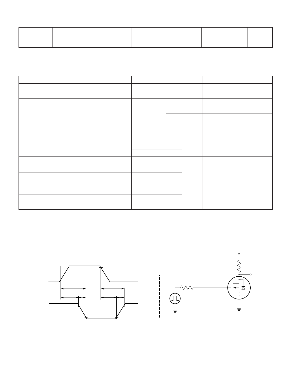
Switching Waveforms and Test Circuit
INPUT
OUTPUT
10V
0V
V
0V
10%
t
(ON)
t
d(ON)
DD
10%
90%
t
r
90%
t
d(OFF)
t
(OFF)
t
F
90%
10%
7-14
PULSE
GENERATOR
R
gen
INPUT
V
DD
R
L
OUTPUT
D.U.T.
 Loading...