

Page 1
New Product
N-Channel 90-V (D-S) MOSFET
2N6661-2
Vishay Siliconix
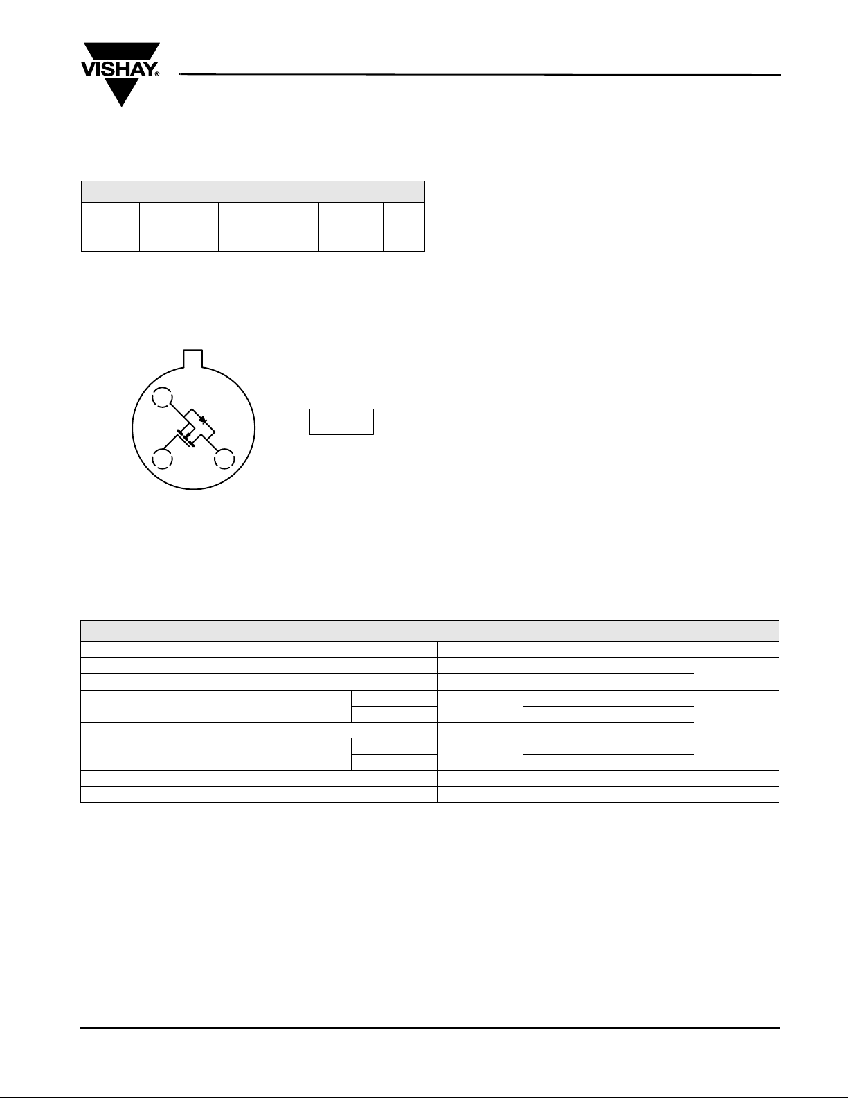
PRODUCT SUMMARY
Part
Number
2N6661-2 90
V
DS
TO-205AD
S
1
2 3
min. (V) R
(TO-39)
To p View
2N6661-2
DS(on)
4 at V
max. (Ω)V
= 10 V
GS
“S” = Siliconix Logo
f = Factory Code
DG
xxyy = Date Code
(V) ID (A)
GS(th)
0.8 to 2 0.86
Device Marking
Side View
2N6661-2
“S” fxxyy
FEATURES
• Low On-Resistance: 3.6 Ω
• Low Threshold: 1.6 V
• Low Input Capacitance: 35 pF
• Fast Switching Speed: 6 ns
• Low Input and Output Leakage
BENEFITS
• Low Offset Voltage
• Low-Voltage Operation
• Easily Driven Without Buffer
• High-Speed Circuits
• Low Error Voltage
APPLICATIONS
• Direct Logic-Level Interface: TTL/CMOS
• Drivers: Relays, Solenoids, Lamps, Hammers, Displays,
Memories, Transistors, etc.
• Battery Operated Systems
• Solid-State Relays
ABSOLUTE MAXIMUM RATINGS TA = 25 °C, unless otherwise noted
Parameter Symbol 2N6661-2 Unit
Drain-Source Voltage
Gate-Source Voltage
Continuous Drain Current (T
Pulsed Drain Current
Power Dissipation
Thermal Resistance, Junction-to-Ambient
Operating Junction and Storage Temperature Range
Notes:
a. Pulse width limited by maximum junction temperature.
b. This parameter not registered with JEDEC.
= 150 °C)
J
a
b
= 25 °C
T
C
= 100 °C
T
C
= 25 °C
T
C
T
= 25 °C
A
V
DS
V
GS
I
D
I
DM
P
D
R
thJA
T
, T
J
stg
90
± 20
0.86
0.54
± 3
6.25
0.725
170
- 65 to 150
V
A
W
°C/W
°C
Document Number: 68632
S-81302-Rev. A, 09-Jun-08
www.vishay.com
1
Page 2
New Product
2N6661-2
Vishay Siliconix
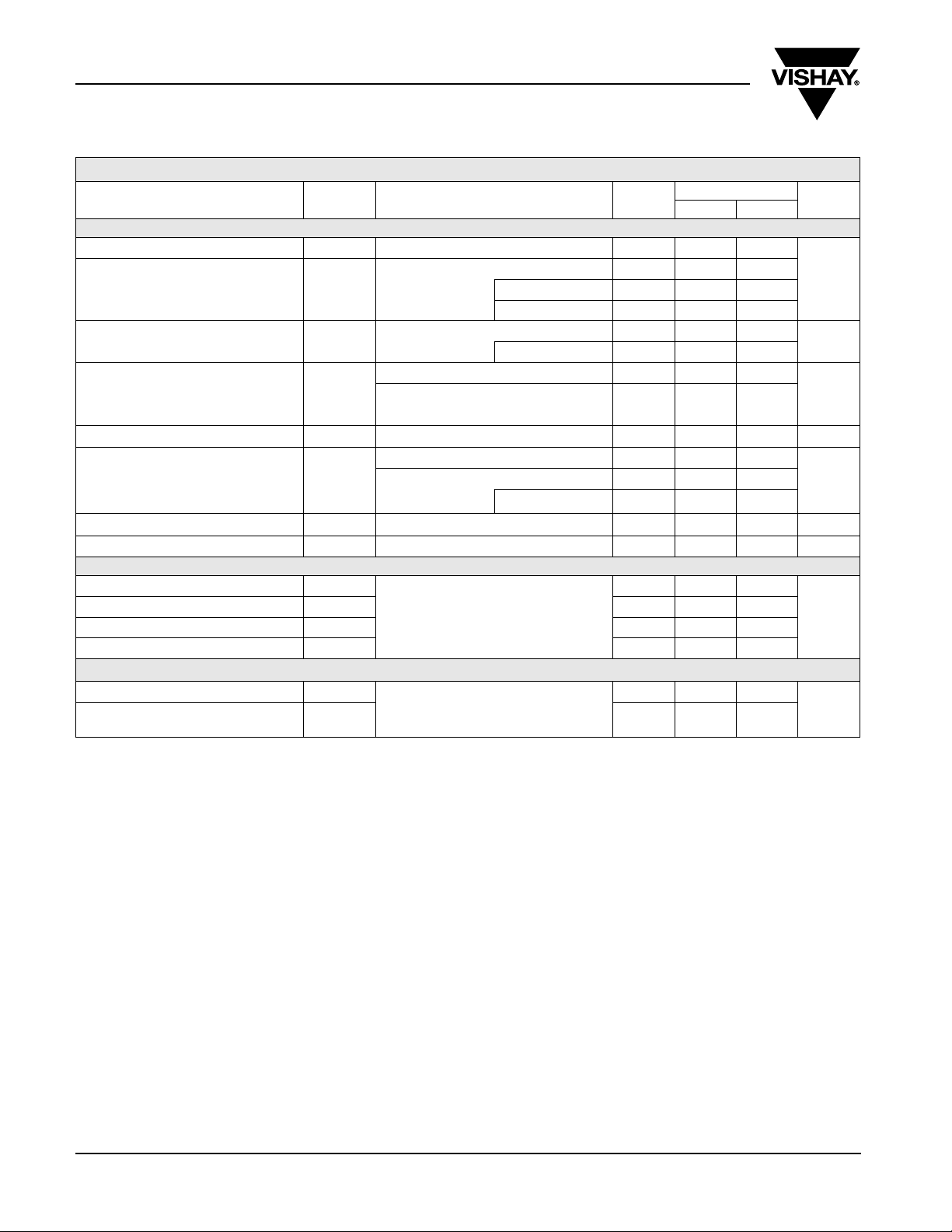
SPECIFICATIONS TJ = 25 °C, unless otherwise noted
Parameter Symbol Test Conditions Typ.
Static
Drain-Source Breakdown Voltage
Gate-Threshold Voltage
Gate-Body Leakage
Zero Gate Voltage Drain Current
On-State Drain Current
Drain-Source On-Resistance
Forward Transconductance
b
b
b
Diode Forward Voltage
V
V
GS(th)
I
GSS
I
I
D(on)
R
DS(on)
V
DS
DSS
g
fs
SD
Dynamic
Input Capacitance
Output Capacitance
Reverse Transfer Capacitance
Drain-Source Capacitance
Switching
c
Tur n - On T i m e
Turn-Off Time
C
C
C
C
t
t
iss
oss
rss
ds
ON
OFF
Notes:
a. For DESIGN AID ONLY, not subject to production testing.
b. Pulse test; pulse width ≤ 300 µs, duty cycle ≤ 2 %.
c. Switching time is essentially independent of operating temperature.
d. This parameter not registered with JEDEC.
VGS = 0 V, ID = 10 µA
V
= VGS, ID = 1 mA
DS
T
= - 55 °C
A
T
= 125 °C
A
VDS = 0 V, VGS = ± 20 V
T
= 125 °C
A
VDS = 72 V, VGS = 0 V
= 72 V, VGS = 0 V
V
DS
T
= 125 °C
A
VDS = 10 V, VGS = 10 V
VGS = 5 V, ID = 0.3 A
V
= 10 V, ID = 1 A
GS
T
= 125 °Cd
A
VDS = 7.5 V, ID = 0.475 A
IS = 0.86 A, V
VDS = 25 V, V
GS
GS
= 0 V
= 0 V,
f = 1 MHz
VDD = 25 V, RL = 23 Ω
≅ 1 A, V
I
D
R
= 23 Ω
GS
GEN
= 10 V
a
Unit Min. Max.
125 90
Limits
1.6 0.8 2
1.8 2.5
V
1.3 0.3
± 100
± 500
nA
1
100
µA
1.8 A
3.8 5.3
3.6 4
Ω
6.7 7.5
340 170 mS
0.9 0.7 1.4 V
35 50
15 40
210
pF
30
610
810
ns
Stresses beyond those listed under “Absolute Maximum Ratings” may cause permanent damage to the device. These are stress ratings only, and functional operation
of the device at these or any other conditions beyond those indicated in the operational sections of the specifications is not implied. Exposure to absolute maximum
rating conditions for extended periods may affect device reliability.
www.vishay.com
2
Document Number: 68632
S-81302-Rev. A, 09-Jun-08
Page 3
New Product
2N6661-2
Vishay Siliconix
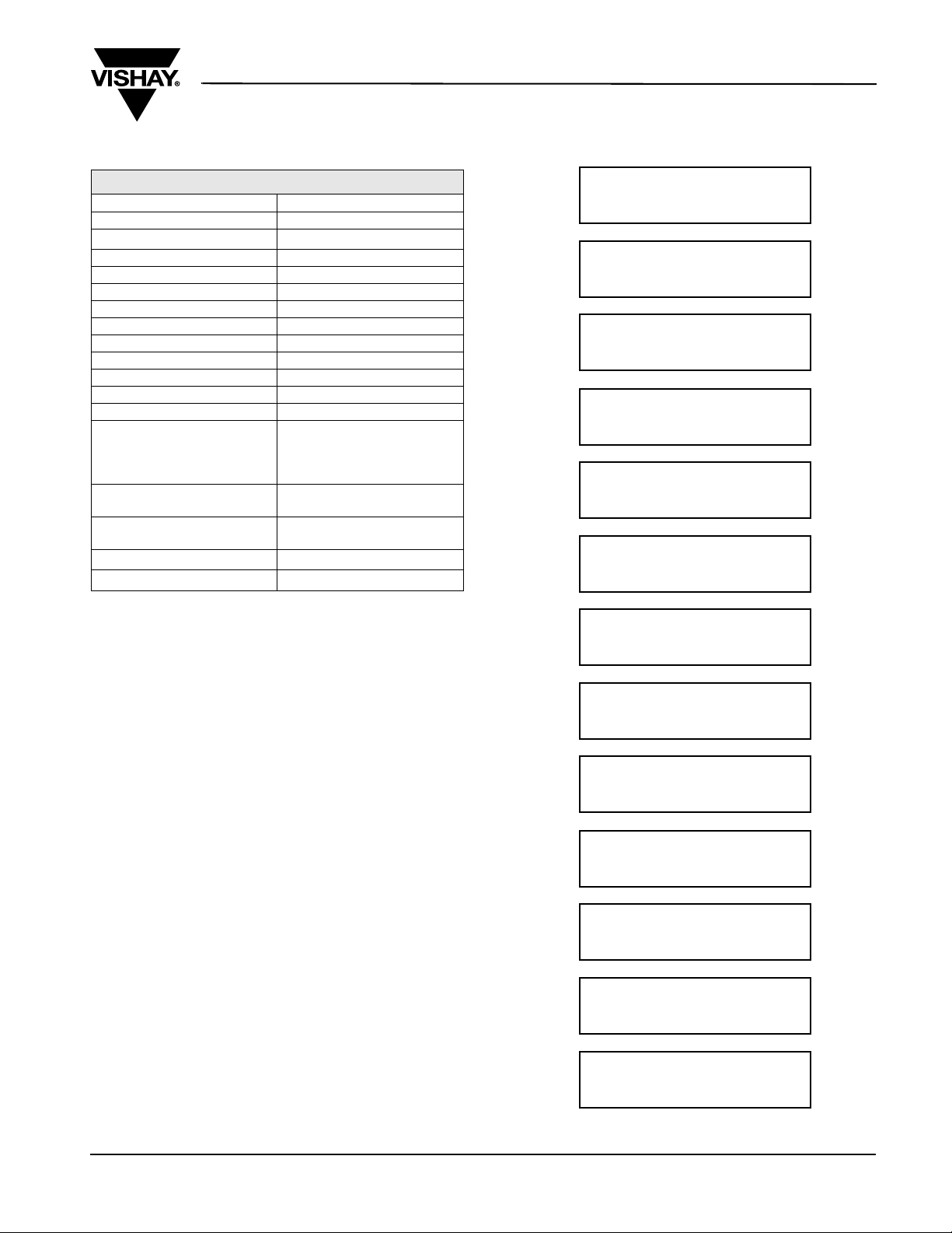
PROCESS FLOW
Description
Internal Visual M-2072 Condition B
Die Shear
Stabilization Bake M-1032
Temperature Cycling M-1051 Condition G
Constant Acceleration M-2006
Interim Electrical Go-no-Go
Burn-In (HTGB) M1042_Condition B (48 h)
Burn-In (HTRB) M1042_Condition A (160 h)
Final Electrical Go-no-Go
Fine Leak M-1071 Condition G1
Gross Leak M-1071 Condition C1
External Visual M-2071 S/S = 45/0
Group A
Per MIL-PRF-19500
Sampling plan for Group A
Inspection
Group B
Per MIL-PRF-19500
Group C
Per MIL-PRF-19500
Deltas Option
Solder Dip Option
Notes:
a. Test performed on line during assembly procedure (monitor).
b. Per spec is a reference to Vishay Siliconix data sheet or customer
SCD whichever applies.
MIL-STD 750 Methods
a
M-2017
per spec.
per spec.
per spec.
per spec.
per spec.
b
b
MANUFACTURING FLOW
Internal Visual
M-2072 Condition B
↓
M2017 (assembly monitor)
Die Shear
↓
High Temp Life (Stab Bake)
M-1032
↓
Temperature Cycling
M-1051 Condition G
↓
Constant Acceleration
(SI imposed) M-2006
↓
Interim Electrical
Go-no-Go
↓
Burn-in HTGB / HTRB
M-1042 48 h/160 h
↓
Final Electrical
Go-no-Go
↓
Fine and Gross Leak
M-1071 Condition G1
and Condition C1
↓
External Visual
M-2071 S/S = 45/0
↓
Per MIL-PRF-19500 Sampling plan
for Group A Inspection Go-no-Go
Group A
↓
Per MIL-PRF-19500 Table E-VIB
Group B
Go-no-Go
↓
Per MIL-PRF-19500 Table E-VII
Group C
Go-no-Go
Document Number: 68632
S-81302-Rev. A, 09-Jun-08
www.vishay.com
3
Page 4
New Product
2N6661-2
Vishay Siliconix
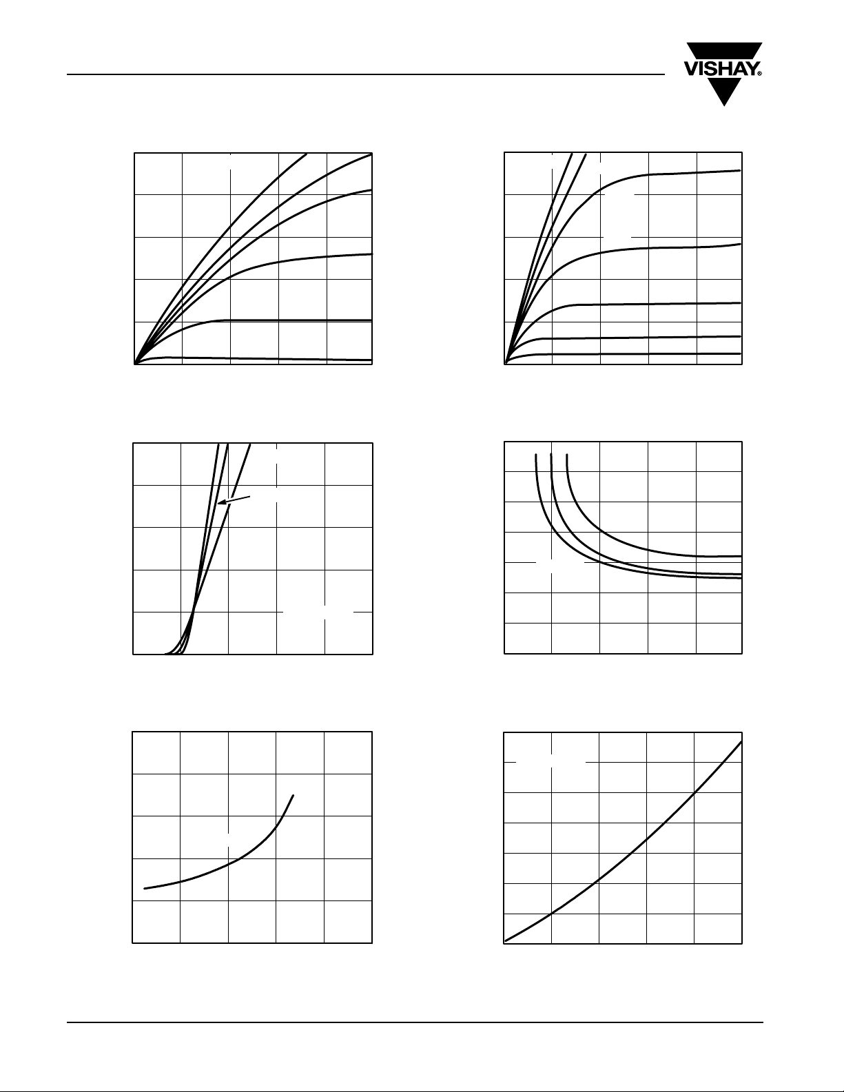
TYPICAL CHARACTERISTICS 25 °C, unless otherwise noted
1.0
0.8
0.6
0.4
- Drain Current (A)
D
I
0.2
0.5
0.4
0.3
0.2
- Drain Current (A)
D
I
0.1
VGS = 10 V
6 V
5 V
4 V
3 V
0
0 1.0 2.0 3.0 4.0 5.0
VDS - Drain-to-Source Voltage (V)
2 V
Ohmic Region Characteristics
125 °C
25 °C
VDS= 15 V
100
80
60
40
- Drain Current (mA)
D
I
20
- On-Resistance (Ω)
DS(on)
R
VGS = 3 V
0
0 0.4 0.8 1.2 1.6 2.0
2.8 V
2.6 V
2.4 V
2.2 V
2.0 V
1.8 V
VDS - Drain-to-Source Voltage (V)
Output Characteristics for Low Gate Drive
7
6
5
4
3
2
1
ID= 0.1 A
0.5 A
1.0 A
0
10
8
6
4
- Drain-Source On-Resistance (Ω)
2
DS(on)
R
0
www.vishay.com
4
468
VGS - Gate-Source Voltage (V)
Transfer Characteristics
VGS= 10 V
1.0 1.5 2.0
ID - Drain Current (A)
On-Resistance vs. Drain Current
0
0120
048 12 16 20
VGS - Gate-Source Voltage (V)
On-Resistance vs. Gate-to-Source Voltage
2.25
2.00
1.75
1.50
1.25
(Normalized)
- Drain-Source On-Resistance
1.00
DS(on)
0.75
R
5 .25.00
0.50
VGS= 10 V
- 50 - 10 30 70 110 150
TJ - Junction Temperature (°C)
Normalized On-Resistance vs. Junction Temperature
Document Number: 68632
S-81302-Rev. A, 09-Jun-08
Page 5
New Product
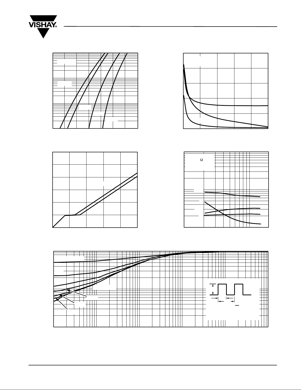
TYPICAL CHARACTERISTICS 25 °C, unless otherwise noted
10
VGS= 5 V
125
100
2N6661-2
Vishay Siliconix
VGS= 0 V
f = 1 MHz
- Drain Current (mA)
0.1
D
I
0.01
15.0
12.5
10.0
7.5
5.0
- Gate-to-Source Voltage (V)
GS
2.5
V
1
0.5
ID= 1.0 A
TJ = 150
125 °C
25 °C
1.0 1.5
VGS - Gate-to-Source Voltage (V)
Threshold Region
VDS= 45 V
- 55 °C
72 V
2.0
75
50
C - Capacitance (pF)
25
C
0
100
VDD = 25 V
R
= 23
L
VGS = 0 to 10 V
= 1.0 A
I
D
10
t - Switching Time (ns)
t
d(off)
t
d(on)
C
iss
C
oss
rss
20 30 40
VDS - Drain-to-Source Voltage (V)
Capacitance
t
r
t
f
05010
0
200 300 400
0050010
Qg - Total Gate Charge (pC)
Gate Charge
1
211.0
ID - Drain Current (A)
Load Condition Effects on Switching
1.0
Duty Cycle = 0.5
0.2
0.1
0.1
Thermal Impedance
Normalized Effective Transient
Single Pulse
0.05
0.02
0.01
Notes:
P
DM
t
1
t
2
t
1. Duty Cycle, D =
2. Per Unit Base = R °
3. T
- TC = PDMZ
JM
t
thJC
thJC
1
2
= 20 C/W
(t)
0.01
0.1 10 K
0010.1 K 101
t1- Square Wave Pulse Duration (s)
Normalized Effective Transient Thermal Impedance, Junction-to-Case (2N6661-2)
Vishay Siliconix maintains worldwide manufacturing capability. Products may be manufactured at one of several qualified locations. Reliability data for Silicon
Technology and Package Reliability represent a composite of all qualified locations. For related documents such as package/tape drawings, part marking, and
reliability data, see http://www.vishay.com/ppg?68632.
Document Number: 68632
www.vishay.com
S-81302-Rev. A, 09-Jun-08
5
Page 6
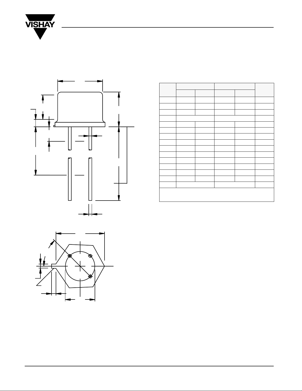
TO-205AD (TO-39 TALL LID)
CD
Q
P
L1
L2
LU
Seating
Plane
LL
CH
Package Information
Vishay Siliconix
INCHES MILLIMETERS
Dim Min Max Min Max
CD
CH
HD
LC
LD
LL
LU
L1
L2
P
Q
TL
TW
m
Dimensions (see notes 1, 2, 9, 11, 12)
ECN: S-40373—Rev. C, 15-Mar-04
DWG: 5511
0.305 0.335 7.75 8.51
0.240 0.260 6.10 6.60
0.335 0.370 8.51 9.40
0.200 TP 5.08 TP 6
0.016 0.021 0.41 0.53 7, 8
0.500 0.750 12.70 19.05 7, 8
0.016 0.019 0.41 0.48 7, 8
— 0.050 — 1.27 7, 8
0.250 — 6.35 — 7, 8
0.100 — 2.54 — 5
— 0.050 — 1.27 4
r
— 0.010 — 0.25 9
0.029 0.045 0.74 1.14 3
0.028 0.034 0.71 0.86 2
45_ TP 45_ TP 6
Notes
TW
LD
NOTES:
1. Dimensions are in inches. Metric equivalents are given for general
HD
∝
C
L
r
TL
12
3
LC
information only.
2. Beyond radius (r) maximum, TW shall be held for a minimum length of 0.011
(0.028 mm).
3. Dimension TL measured from maximum HD.
4. Outline in this zone is not controlled.
5. Dimension CD shall not vary more than 0.010 (0.25 mm) in zone P. This
zone is controlled for automatic handling.
6. Leads at guage plane 0.054+0.001, −0.000 (1.37+0.03, −0.00 mm) below
seating plane shall be within 0.007 (0.18 mm) radius of true position (TP) at
maximum material condition (MMC) relative to tab at MMC.
7. LU applies between L1 and L2, LD applies between L2 and L maximum.
Diameter is uncontrolled in L1 and beyond LL minimum.
8. All three leads.
9. Radius (r) applies to both inside corners of tab.
10. Drain is electrically connected to the case.
Document Number: 71367
09-Mar-04
www.vishay.com
1
Page 7

Legal Disclaimer Notice
Vishay
Disclaimer
ALL PRODUCT, PRODUCT SPECIFICATIONS AND DATA ARE SUBJECT TO CHANGE WITHOUT NOTICE TO IMPROVE
RELIABILITY, FUNCTION OR DESIGN OR OTHERWISE.
Vishay Intertechnology, Inc., its affiliates, agents, and employees, and all persons acting on its or their behalf (collectively,
“Vishay”), disclaim any and all liability for any errors, inaccuracies or incompleteness contained in any datasheet or in any other
disclosure relating to any product.
Vishay makes no warranty, representation or guarantee regarding the suitability of the products for any particular purpose or
the continuing production of any product. To the maximum extent permitted by applicable law, Vishay disclaims (i) any and all
liability arising out of the application or use of any product, (ii) any and all liability, including without limitation special,
consequential or incidental damages, and (iii) any and all implied warranties, including warranties of fitness for particular
purpose, non-infringement and merchantability.
Statements regarding the suitability of products for certain types of applications are based on Vishay’s knowledge of typical
requirements that are often placed on Vishay products in generic applications. Such statements are not binding statements
about the suitability of products for a particular application. It is the customer’s responsibility to validate that a particular
product with the properties described in the product specification is suitable for use in a particular application. Parameters
provided in datasheets and/or specifications may vary in different applications and performance may vary over time. All
operating parameters, including typical parameters, must be validated for each customer application by the customer’s
technical experts. Product specifications do not expand or otherwise modify Vishay’s terms and conditions of purchase,
including but not limited to the warranty expressed therein.
Except as expressly indicated in writing, Vishay products are not designed for use in medical, life-saving, or life-sustaining
applications or for any other application in which the failure of the Vishay product could result in personal injury or death.
Customers using or selling Vishay products not expressly indicated for use in such applications do so at their own risk and agree
to fully indemnify and hold Vishay and its distributors harmless from and against any and all claims, liabilities, expenses and
damages arising or resulting in connection with such use or sale, including attorneys fees, even if such claim alleges that Vishay
or its distributor was negligent regarding the design or manufacture of the part. Please contact authorized Vishay personnel to
obtain written terms and conditions regarding products designed for such applications.
No license, express or implied, by estoppel or otherwise, to any intellectual property rights is granted by this document or by
any conduct of Vishay. Product names and markings noted herein may be trademarks of their respective owners.
Document Number: 91000 www.vishay.com
Revision: 11-Mar-11 1
 Loading...