

Page 1
SILICO N NPN POW ER DAR L IN GTO N TRA NS IS T OR
■ SGS-THOMSON PREFERRED SALESTYPE
■ HIGH GAIN
■ NPN DARLINGTON
■ HIGH CURRENT
■ HIGH DISSIPATION
■ INTEGRATED ANTIPARALLEL
COLLECTOR-EMITTER DIODE
2N6059
APPLICATIONS
■ LINEAR AND SWITCHING INDUSTRIAL
EQUIPMENT
DESCRIPTION
The 2N6059 is a silicon epitaxial-base NPN
transistor in monolithic Darlington configuration
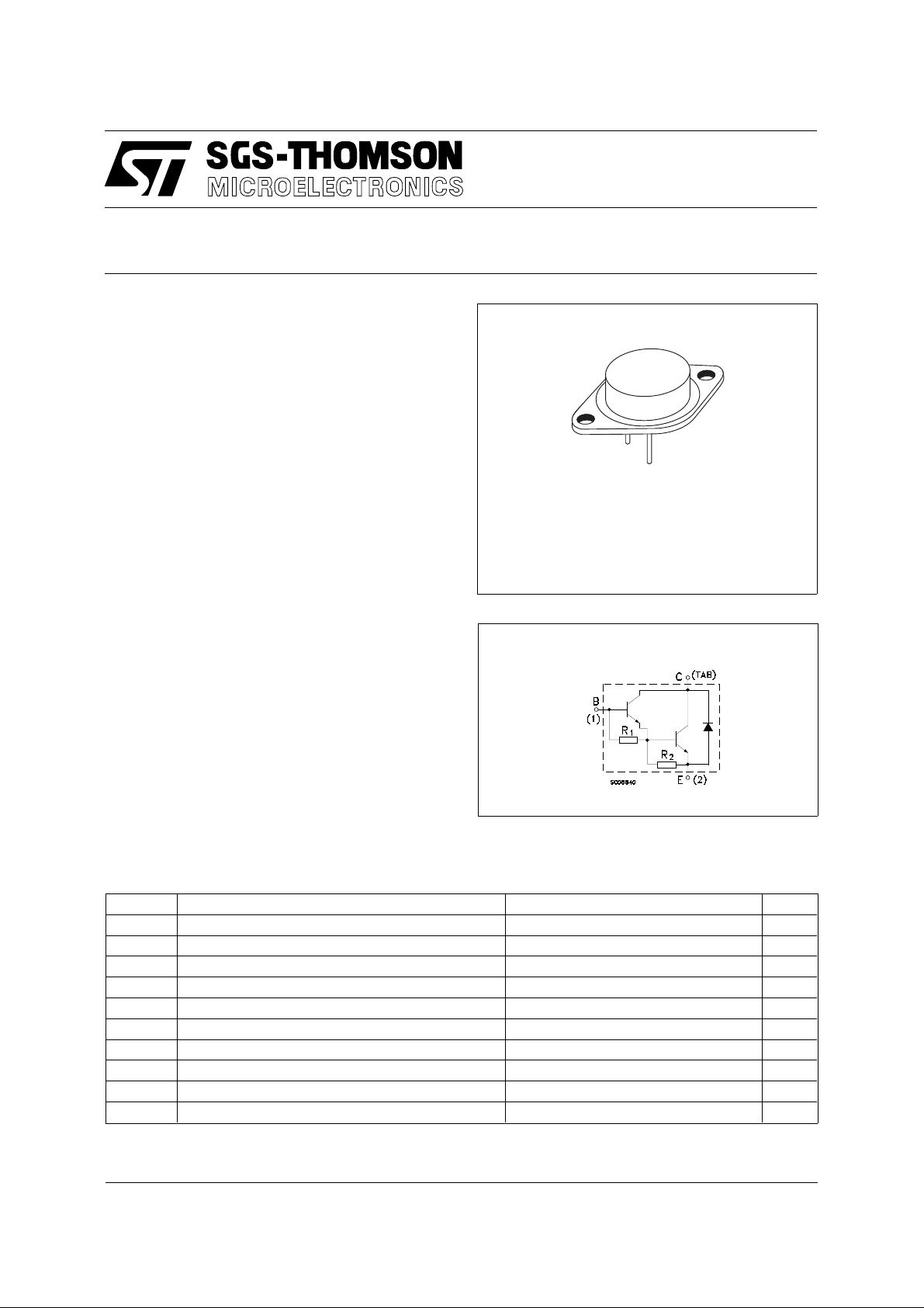
mounted in Jedec TO -3 metal case.
It is inteded for use in power linear and low
frequency switching applications.
ABSOL UT E MAXIMU M RATINGS
1
2
TO-3
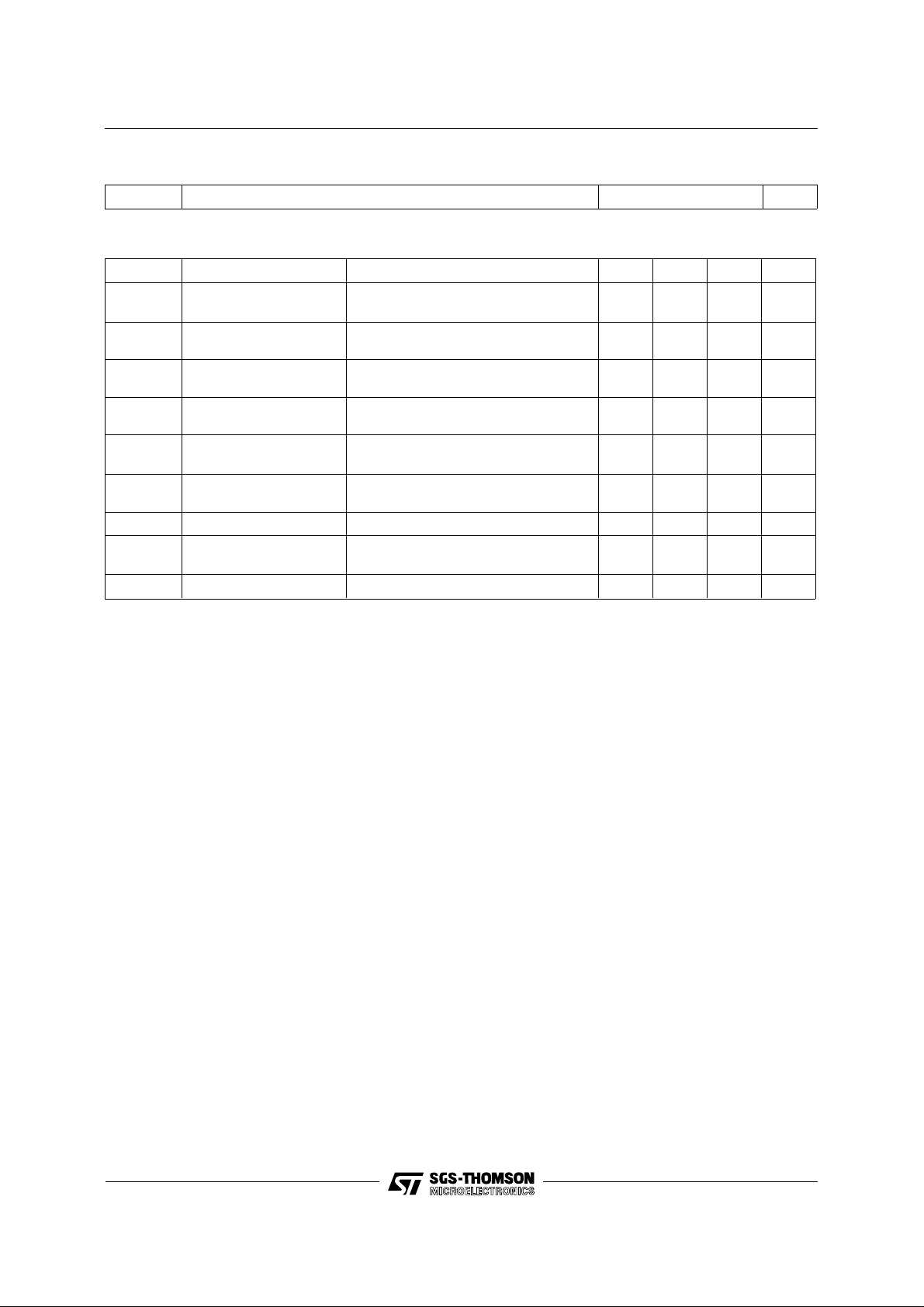
INTERNAL SCHEMATIC DIAGRAM
R1 Typ. = 6 KΩ R2 Typ. = 55 Ω
Symbol Parameter Value Unit
V
V
V
V
I
P
T
For PNP types voltage and current values are negative.
Collector-Base Voltage (IE = 0) 100 V
CBO
Collector-Emitter Voltage (VBE = -1.5V) 100 V
CEX
Collector-Emitter Voltage (IB = 0) 100 V
CEO
Emitter-Base Voltage (IC = 0) 5 V
EBO
Collector Current 12 A
I
C
Collector Peak Current 20 A
CM
Base Current 0.2 A
I
B
Total Dissipation at Tc ≤ 25 oC 150 W
tot
Storage Temperature -65 to 200
stg
Max. Operating Junction Temperature 200
T
j
June 1997
o
C
o
C
1/4
Page 2
2N6059
THERMAL DATA
R
thj-case
Thermal Resistance Junction-case Max 1.17
o
C/W
ELECTRICAL CHARACTERISTICS (T
= 25 oC unless otherwise specified)
case
Symbol Parameter Test Conditions Min. Typ. Max. Unit
I
CEX
I
CEO
I
EBO
V
CEO(sus)
Collector Cut-off
Current (V
= -1.5V)
BE
Collector Cut-off
Current (I
= 0)
B
Emitter Cut-off Current
(I
= 0)
C
∗ Collector-Emitter
= rated V
V
CE
VCE = rated V
= 50 V 1 mA
V
CE
= 5 V 2 mA
V
EB
CEX
Tc = 150 oC
CEX
0.5
5
IC = 100 mA 100 V
Sustaining Voltage
V
CE(sat)
V
BE(sat)
∗ Collector-Emitter
Saturation Voltage
∗ Base-Emitter
IC = 6 A IB = 24 mA
I
= 12 A IB = 120 mA
C
2
3
IC = 12 A IB = 120 mA 4 V
Saturation Voltage
∗ Base-Emitter Voltage IC = 6 A VCE = 3 V 2.8 V
V
BE
hFE∗ DC Current Gain IC = 6 A VCE = 3 V
I
= 12 A VCE = 3 V
C
f
∗ Pulsed: Pulse duration = 300 µs, duty cycle 1.5 %
Transition frequency IC = 5 A VCE = 3 V f =1 MHz 4 MHz
T
750
100
mA
mA
V
V
2/4
Page 3

P003F
TO-3 MECHANICAL DATA
2N6059
DIM.
MIN. TYP. MAX. MIN. TYP. MAX.
A 11.00 13.10 0.433 0.516
B 0.97 1.15 0.038 0.045
C 1.50 1.65 0.059 0.065
D 8.32 8.92 0.327 0.351
E 19.00 20.00 0.748 0.787
G 10.70 11.10 0.421 0.437
N 16.50 17.20 0.649 0.677
P 25.00 26.00 0.984 1.023
R 4.00 4.09 0.157 0.161
U 38.50 39.30 1.515 1.547
V 30.00 30.30 1.187 1.193
mm inch
P
A
G
U
V
N
O
B
D
C
E
R
3/4
Page 4

2N6059
Information furnished is believed to be accurate and reliable. However, SGS-THOMSON Microelectronics assumes no responsability for the
consequences of use of such information nor for any infringement of patents or other rights of third parties which may results from its use. No
license is granted by implication or ot h erwise under any patent or patent rights of SGS-THOMSON Microelectronics. Specifi cations mentioned
in this publication are subject to change without notice. This publication sup ersedes and replaces all information previously supplied.
SGS-THOMSON Microelectronics products are not authorized for use as critical components in life support devices or systems wi thout express
written approval of SGS-THOMSON Microelectonics.
© 1997 SGS-THOMSON Microelectronics - Printed in Italy - All Rights Reserved
Australia - Brazil - Canada - China - France - Germany - Hong Kong - Italy - Japan - Korea - Malaysia - Malta - Morocco - The Netherlands -
Singapore - Spain - Sweden - Switzerland - Taiwan - Thailand - United Kingdom - U.S.A
SGS-THOMSON Microelectronics GROUP OF COMPANIES
. . .
4/4
 Loading...