

Page 1
Î
Î
Î
Î
Î
Î
Î
Î
Î
Î
Î
Î
Î
Î
Î
Î
Î
SEMICONDUCTOR TECHNICAL DATA
"
Order this document
by 2N6052/D
!
. . . designed for general–purpose amplifier and low frequency switching applications.
• High DC Current Gain —
hFE = 3500 (Typ) @ IC = 5.0 Adc
• Collector–Emitter Sustaining Voltage — @ 100 mA
V
CEO(sus)
V
CEO(sus)
• Monolithic Construction with Built–In Base–Emitter Shunt Resistors
MAXIMUM RATINGS (1)
ОООООООООО
Collector–Emitter Voltage
Collector–Base Voltage
Emitter–Base voltage
Collector Current — Continuous
ОООООООООО
Base Current
Total Device Dissipation
@TC = 25_C
ОООООООООО
Derate above 25_C
Operating and Storage Junction
ОООООООООО
T emperature Range
THERMAL CHARACTERISTICS
Thermal Resistance, Junction to Case
(1) Indicates JEDEC Registered Data.
= 80 Vdc (Min) — 2N6058
= 100 Vdc (Min) — 2N6052, 2N6059
Rating
Peak
Characteristic
ÎÎ
Symbol
V
CEO
V
CB
V
EB
I
C
ÎÎ
I
B
P
ÎÎ
TJ, T
ÎÎ
Symbol
5.0
12
20
0.2
150
0.857
Rating
2N6052
ÎÎ
2N6059
100
100
1.17
Î
Unit
Vdc
Vdc
Vdc
Adc
Î
Adc
Watts
Î
W/_C
_
C
Î
Unit
_
C/W
ÎÎ
2N6058
80
80
ООООО
D
ООООО
–65 to +200_C
ООООО
R
stg
θJC
*Motorola Preferred Device
DARLINGTON
12 AMPERE
COMPLEMENTARY
SILICON
POWER TRANSISTORS
80–100 VOL TS
150 WATTS
CASE 1–07
TO–204AA
(TO–3)
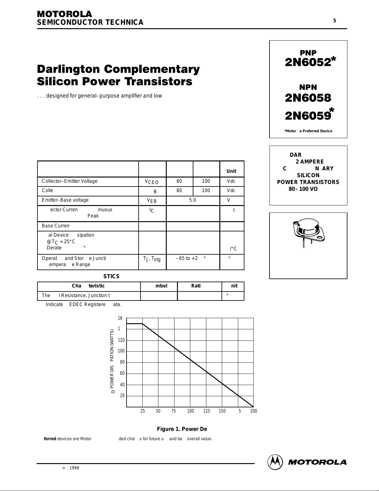
160
140
120
100
80
60
40
, POWER DISSIPATION (W ATTS)
D
P
20
0
0 25 50 75 100 125 150 200
TC, CASE TEMPERATURE (°C)
Figure 1. Power Derating
Preferred devices are Motorola recommended choices for future use and best overall value.
Motorola, Inc. 1998
Motorola Bipolar Power Transistor Device Data
175
1
Page 2
2N6052
ÎÎÎÎ
Î
Î
ÎÎÎÎ
Î
Î
Î
Î
Î
Î
Î
Î
Î
ÎÎÎÎ
Î
Î
Î
Î
Î
Î
ÎÎÎÎ
Î
Î
Î
Î
Î
Î
Î
Î
Î
ÎÎÎÎ
Î
Î
Î
Î
Î
Î
ÎÎÎÎ
Î
Î
Î
Î
Î
Î
Î
Î
Î
Î
ÎÎÎÎ
Î
Î
Î
Î
Î
Î
Î
Î
Î
ÎÎÎÎ
Î
Î
Î
Î
ÎÎÎÎ
Î
Î
ÎÎÎÎ
Î
Î
Î
Î
Î
Î
Î
Î
ÎÎÎÎ
Î
ÎÎÎÎ
Î
Î
Î
Î
*ELECTRICAL CHARACTERISTICS (T
= 25_C unless otherwise noted)
C
Characteristic
OFF CHARACTERISTICS
Collector–Emitter Sustaining Voltage (1)
(IC = 100 mAdc, IB = 0) 2N6058
ООООООООООООООООООООО
ООООООООООООООООООООО
2N6052, 2N6059
Collector Cutoff Current
(VCE = 40 Vdc, IB = 0) 2N6058
ООООООООООООООООООООО
(VCE = 50 Vdc, IB = 0) 2N6052, 2N6059
Collector Cutoff Current
(VCE = Rated V
ООООООООООООООООООООО
(VCE = Rated V
ООООООООООООООООООООО
Emitter Cutoff Current
ООООООООООООООООООООО
(VBE = 5.0 Vdc, IC = 0)
CEO
CEO
, V
, V
= 1.5 Vdc)
BE(off)
= 1.5 Vdc, TC = 150_C)
BE(off)
ON CHARACTERISTICS (1)
DC Current Gain
(IC = 6.0 Adc, VCE = 3.0 Vdc)
ООООООООООООООООООООО
(IC = 12 Adc, VCE = 3.0 Vdc)
ООООООООООООООООООООО
Collector–Emitter Saturation Voltage
ООООООООООООООООООООО
(IC = 6.0 Adc, IB = 24 mAdc)
ООООООООООООООООООООО
(IC = 12 Adc, IB = 120 mAdc)
Base–Emitter Saturation Voltage
(IC = 12 Adc, IB = 120 mAdc)
ООООООООООООООООООООО
Base–Emitter On Voltage
(IC = 6.0 Adc, VCE = 3.0 Vdc)
DYNAMIC CHARACTERISTICS
Magnitude of Common Emitter Small–Signal Short Circuit Forward
ООООООООООООООООООООО
Current Transfer Ratio
(IC = 5.0 Adc, VCE = 3.0 Vdc, f = 1.0 MHz)
ООООООООООООООООООООО
Output Capacitance 2N6052
(VCB = 10 Vdc, IE = 0, f = 0.1 MHz) 2N6058/2N6059
Small–Signal Current Gain
ООООООООООООООООООООО
(IC = 5.0 Adc, VCE = 3.0 Vdc, f = 1.0 kHz)
*Indicates JEDEC Registered Data.
(1) Pulse test: Pulse Width = 300 µs, Duty Cycle = 2.0%.
Symbol
V
CEO(sus)
ÎÎÎ
ÎÎÎ
I
CEO
ÎÎÎ
I
CEX
ÎÎÎ
ÎÎÎ
I
EBO
ÎÎÎ
h
FE
ÎÎÎ
ÎÎÎ
V
CE(sat)
ÎÎÎ
ÎÎÎ
V
BE(sat)
ÎÎÎ
V
BE(on)
|hfe|
ÎÎÎ
ÎÎÎ
C
ob
h
fe
ÎÎÎ
Min
ÎÎ
80
100
ÎÎ
—
ÎÎ
—
—
ÎÎ
ÎÎ
—
ÎÎ
ÎÎ
750
100
ÎÎ
ÎÎ
—
ÎÎ
—
—
ÎÎ
—
4.0
ÎÎ
ÎÎ
—
—
300
ÎÎ
Max
ÎÎ
—
—
ÎÎ
1.0
ÎÎ
1.0
0.5
ÎÎ
5.0
ÎÎ
2.0
ÎÎ
ÎÎ
18,000
—
ÎÎ
ÎÎ
2.0
ÎÎ
3.0
4.0
ÎÎ
2.8
—
ÎÎ
ÎÎ
500
300
—
ÎÎ
Unit
Vdc
ÎÎ
ÎÎ
mAdc
ÎÎ
mAdc
ÎÎ
ÎÎ
mAdc
ÎÎ
—
ÎÎ
ÎÎ
Vdc
ÎÎ
ÎÎ
Vdc
ÎÎ
Vdc
MHz
ÎÎ
ÎÎ
pF
—
ÎÎ
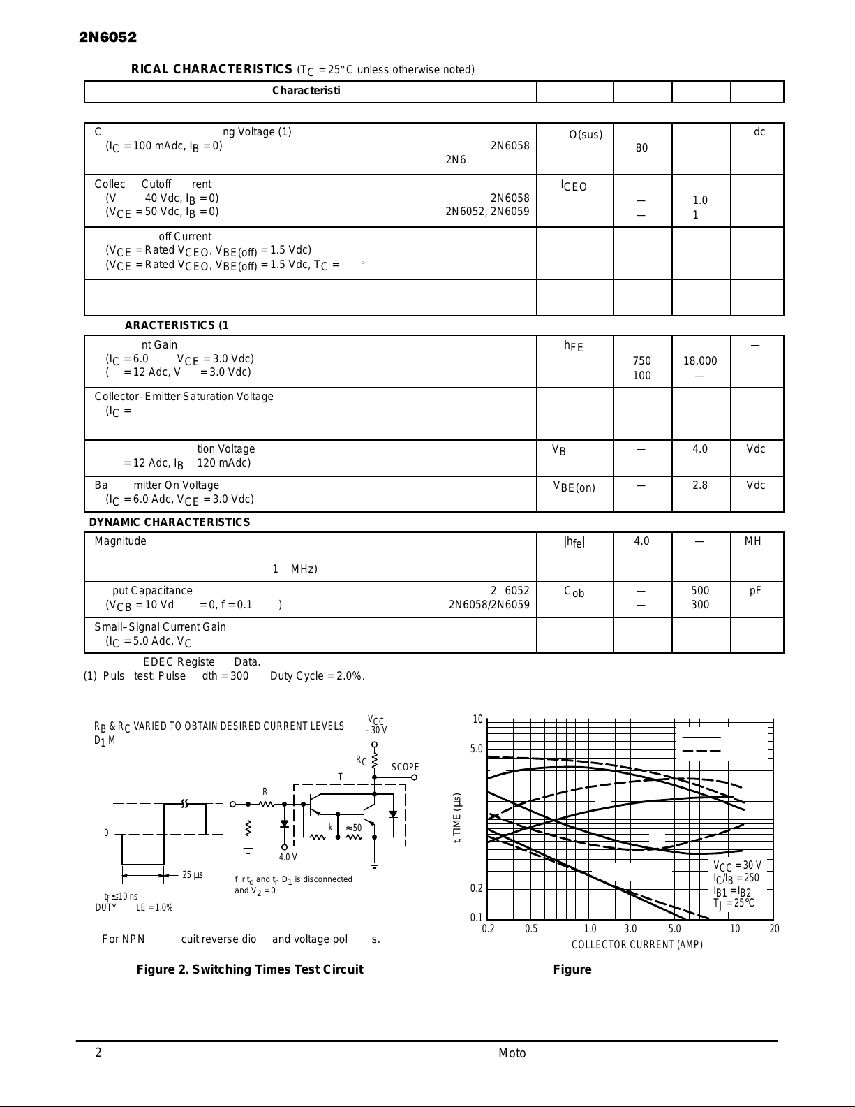
RB & RC VARIED TO OBTAIN DESIRED CURRENT LEVELS
D1 MUST BE FAST RECOVER Y TYPE, eg:
1N5825 USED ABOVE IB
MSD6100 USED BELOW IB
V
2
approx
+8.0 V
0
V
1
approx
–8.0 V
tr, tf
≤
10 ns
DUTY CYCLE = 1.0%
25
≈
100 mA
≈
100 mA
51
µ
s
for td and tr, D1 is disconnected
and V2 = 0
R
B
D
1
+4.0 V
≈
5.0 k
TUT
≈
For NPN test circuit reverse diode and voltage polarities.
Figure 2. Switching Times Test Circuit
2
50
R
V
–30 V
C
CC
SCOPE
µ
t, TIME ( s)
10
5.0
t
s
2.0
t
f
1.0
t
BE(off)
r
= 0
0.5
td @ V
0.2
0.1
0.2
0.5 1.0 3.0 20
5.0 10
IC, COLLECTOR CURRENT (AMP)
Figure 3. Switching Times
Motorola Bipolar Power Transistor Device Data
2N6052
2N6059
VCC = 30 V
IC/IB = 250
IB1 = I
B2
°
C
TJ = 25
Page 3

1.0
0.7
0.5
2N6052
D = 0.5
0.3
0.2
0.1
0.07
0.05
0.03
RESISTANCE (NORMALIZED)
0.02
r(t), EFFECTIVE TRANSIENT THERMAL
0.01
50
20
10
5.0
2.0
1.0
0.5
, COLLECTOR CURRENT (AMP)
0.2
C
I
0.1
0.05
10
0.2
0.1
0.05
0.02
SINGLE PULSE
0.01
0.02 0.03 0.3 3.0 30 300
TJ = 200°C
VCE, COLLECTOR–EMITTER VOL TAGE (VOLTS)
0.01
0.05 0.1 0.2 0.5 1.0 2.0 5.0 10 20 50 100 200 1000500
0.5 ms
1.0 ms
5.0 ms
SECOND BREAKDOWN LIMITED
BONDING WIRE LIMITED
THERMAL LIMITATION
@TC = 25
°
C (SINGLE PULSE)
20 30
R
(t) = r(t) R
θ
JC
R
θ
JC
D CURVES APPLY FOR POWER
PULSE TRAIN SHOWN
READ TIME AT t
T
J(pk)
t, TIME (ms)
θ
= 1.17°C/W MAX
– TC = P
JC
1
(pk)
θJC(t)
Figure 4. Thermal Response
ACTIVE–REGION SAFE OPERATING AREA
0.1 ms
dc
50 10070
50
20
10
5.0
2.0
1.0
0.5
, COLLECTOR CURRENT (AMP)
0.2
C
I
0.1
0.05
10
0.5 ms
TJ = 200°C
VCE, COLLECTOR–EMITTER VOL TAGE (VOLTS)
P
(pk)
t
1
t
2
DUTY CYCLE, D = t1/t
1.0 ms
5.0 ms
SECOND BREAKDOWN LIMITED
BONDING WIRE LIMITED
THERMAL LIMITATION
@TC = 25
°
C (SINGLE PULSE)
20 30
50 10070
2
0.1 ms
dc
Figure 5. 2N6058
Figure 6. 2N6052, 2N6059
There are two limitations on the power handling ability of a transistor: average junction temperature and second breakdown.
Safe operating area curves indicate IC – VCE limits of the transistor that must be observed for reliable operation; i.e., the transistor must not be subjected to greater dissipation than the curves indicate.
The data of Figures 5, 6 and 7 is based on T
limits are valid for duty cycles to 10% provided T
= 200_C; TC is variable depending on conditions. Second breakdown pulse
J(pk)
v 200_C; T
J(pk)
may be calculated from the data in Figure 4. At high case
J(pk)
temperatures, thermal limitations will reduce the power that can be handled to values less than the limitations imposed by
second breakdown.
C, CAPACITANCE (pF)
500
300
200
100
70
50
0.1
C
ib
2N6052
2N6058/2N6059
1.0 2.0 1005.00.2 0.5
VR, REVERSE VOLTAGE (VOLTS)
Figure 8. Capacitance
TJ = 25°C
C
ob
10 20 50
3000
2000
1000
500
200
100
, SMALL–SIGNAL CURRENT GAIN
fe
h
50
30
1.0
TC = 25°C
VCE = 3.0 V
IC = 5.0 A
2N6052
2N6058/2N6059
2.0 5.0 20 50 100010010
f, FREQUENCY (kHz)
200 500
Figure 7. Small–Signal Current Gain
Motorola Bipolar Power Transistor Device Data
3
Page 4

2N6052
20,000
10,000
5000
3000
2000
1000
, DC CURRENT GAIN
FE
h
500
300
200
3.0
2.6
2.2
PNP
2N6052
VCE = 3.0 V
TJ = 150°C
25°C
–55°C
0.2
0.3 0.5 1.0 2.0 20
IC, COLLECTOR CURRENT (AMP)
3.0 5.0
10
Figure 9. DC Current Gain
TJ = 25°C
IC = 3.0 A
6.0 A
9.0 A
12 A
40,000
20,000
10,000
6,000
4,000
2,000
, DC CURRENT GAIN
FE
h
1,000
600
400
NPN
2N6058, 2N6059
TJ = 150°C
25°C
–55°C
0.2
0.3 0.5 1.0 2.0 2010
IC, COLLECTOR CURRENT (AMP)
3.0
TJ = 25°C
2.6
IC = 3.0 A 6.0 A 9.0 A 12 A
2.2
3.0 5.0
VCE = 3.0 V
, COLLECTOR–EMITTER VOL TAGE (VOLTS)
CE
V
V, VOLTAGE (VOLTS)
1.8
1.4
1.0
0.5
1.0 2.0 10 50
3.0
5.0
IB, BASE CURRENT (mA)
Figure 10. Collector Saturation Region
3.0
TJ = 25°C
2.5
2.0
V
@ IC/IB = 250
BE(sat)
1.5
VBE @ VCE = 3.0 V
1.0
V
@ IC/IB = 250
0.5
0.2
0.3 0.5 1.0 3.0 20
CE(sat)
2.0
IC, COLLECTOR CURRENT (AMP)
1.8
1.4
, COLLECTOR–EMITTER VOL TAGE (VOLTS)
CE
V
20
30
105.0
1.0
0.5 1.0 2.0 10 505.0 203.0 30
3.0
2.5
2.0
1.5
V, VOLTAGE (VOLTS)
1.0
0.5
0.2 0.3 0.5 1.0 3.0 20
Figure 11. “On” Voltages
TJ = 25°C
V
BE(sat)
IB, BASE CURRENT (mA)
@ IC/IB = 250
VBE @ VCE = 3.0 V
V
CE(sat)
2.0 105.0
IC, COLLECTOR CURRENT (AMP)
@ IC/IB = 250
4
Motorola Bipolar Power Transistor Device Data
Page 5

2N6052
P ACKAGE DIMENSIONS
A
N
C
E
2 PLD
0.13 (0.005) Y
U
V
H
L
2
1
G
K
M
–Y–
–T–
B
T
SEATING
PLANE
M
Q
M
–Q–
0.13 (0.005) T
M
M
Y
NOTES:
1. DIMENSIONING AND TOLERANCING PER ANSI
Y14.5M, 1982.
2. CONTROLLING DIMENSION: INCH.
3. ALL RULES AND NOTES ASSOCIATED WITH
REFERENCED TO–204AA OUTLINE SHALL APPLY.
DIM MIN MAX MIN MAX
A 1.550 REF 39.37 REF
B ––– 1.050 ––– 26.67
C 0.250 0.335 6.35 8.51
D 0.038 0.043 0.97 1.09
E 0.055 0.070 1.40 1.77
G 0.430 BSC 10.92 BSC
H 0.215 BSC 5.46 BSC
K 0.440 0.480 11.18 12.19
L 0.665 BSC 16.89 BSC
N ––– 0.830 ––– 21.08
Q 0.151 0.165 3.84 4.19
U 1.187 BSC 30.15 BSC
V 0.131 0.188 3.33 4.77
STYLE 1:
PIN 1. BASE
2. EMITTER
CASE: COLLECTOR
MILLIMETERSINCHES
CASE 1–07
TO–204AA (TO–3)
ISSUE Z
Motorola Bipolar Power Transistor Device Data
5
Page 6

2N6052
Motorola reserves the right to make changes without further notice to any products herein. Motorola makes no warranty , representation or guarantee regarding
the suitability of its products for any particular purpose, nor does Motorola assume any liability arising out of the application or use of any product or circuit, and
specifically disclaims any and all liability, including without limitation consequential or incidental damages. “T ypical” parameters which may be provided in Motorola
data sheets and/or specifications can and do vary in different applications and actual performance may vary over time. All operating parameters, including “Typicals”
must be validated for each customer application by customer’s technical experts. Motorola does not convey any license under its patent rights nor the rights of
others. Motorola products are not designed, intended, or authorized for use as components in systems intended for surgical implant into the body, or other
applications intended to support or sustain life, or for any other application in which the failure of the Motorola product could create a situation where personal injury
or death may occur. Should Buyer purchase or use Motorola products for any such unintended or unauthorized application, Buyer shall indemnify and hold Motorola
and its officers, employees, subsidiaries, affiliates, and distributors harmless against all claims, costs, damages, and expenses, and reasonable attorney fees
arising out of, directly or indirectly, any claim of personal injury or death associated with such unintended or unauthorized use, even if such claim alleges that
Motorola was negligent regarding the design or manufacture of the part. Motorola and are registered trademarks of Motorola, Inc. Motorola, Inc. is an Equal
Opportunity/Affirmative Action Employer.
How to reach us:
USA/EUROPE/Locations Not Listed: Motorola Literature Distribution; JAPAN: Nippon Motorola Ltd.; SPD, Strategic Planning Office, 141,
P.O. Box 5405, Denver, Colorado 80217. 1–303–675–2140 or 1–800–441–2447 4–32–1 Nishi–Gotanda, Shinagawa–ku, Tokyo, Japan. 81–3–5487–8488
Customer Focus Center: 1–800–521–6274
Mfax: RMFAX0@email.sps.mot.com – TOUCHTONE 1–602–244–6609 ASIA/PACIFIC: Motorola Semiconductors H.K. Ltd.; 8B Tai Ping Industrial Park,
Moto rola Fa x Back Syst em – US & Canada ONLY 1–800–774–1848 51 Ting Kok Road, Tai Po, N.T., Hong Kong. 852–26629298
HOME PAGE: http://motorola.com/sps/
6
– http://sps.motorola.com/mfax/
◊
Motorola Bipolar Power Transistor Device Data
Mfax is a trademark of Motorola, Inc.
2N6052/D
 Loading...