

Page 1
2N5911/5912
Vishay Siliconix
Matched N-Channel JFET Pairs
PRODUCT SUMMARY
Part Number V
2N5911 –1 to –5 –25 5 –1 10
2N5912 –1 to –5 –25 5 –1 15
FEATURES BENEFITS APPLICATIONS
D Two-Chip Design
D High Slew Rate
D Low Offset/Drift Voltage
D Low Gate Leakage: 1 pA
D Low Noise
D High CMRR: 85 dB
GS(off)
(V) V
(BR)GSS
Min (V) gfs Min (mS) IG Typ (pA) jV
D Minimum Parasitics Ensuring Maximum
High-Frequency Performance
D Improved Op Amp Speed, Settling Time Accuracy
D Minimum Input Error/Trimming Requirement
D Insignificant Signal Loss/Error Voltage
D High System Sensitivity
D Minimum Error with Large Input Signal
GS1
– V
j Max (mV)
GS2
D Wideband Differential Amps
D High-Speed, Temp-Compensated,
Single-Ended Input Amps
D High Speed Comparators
D Impedance Converters
DESCRIPTION
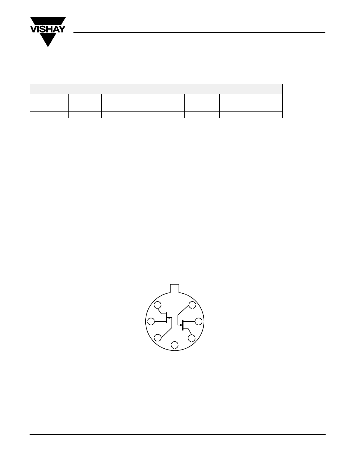
The 2N5911/5912 are matched pairs of JFETs mounted in a
TO-78 package. This two-chip design reduces parasitics and
gives better performance at high frequencies while ensuring
extremely tight matching.
The hermetically-sealed TO-78 package is available with full
military screening per MIL-S-19500 (see Military Information).
S
1
1
D
1
2
3
G
1
ABSOLUTE MAXIMUM RATINGS
TO-78
4
Case
Top View
For similar products see the SO-8 packaged
SST440/SST441, the TO-71 packaged U440/U441, the
low-noise SST/U401 series, and the low-leakage U421/423
data sheets.
G
2
7
D
2
6
5
S
2
Gate-Drain, Gate-Source Voltage –25 V. . . . . . . . . . . . . . . . . . . . . . . . . . . . . . .
Gate-Gate Voltage "80 V. . . . . . . . . . . . . . . . . . . . . . . . . . . . . . . . . . . . . . . . . . . .
Gate Current 50 mA. . . . . . . . . . . . . . . . . . . . . . . . . . . . . . . . . . . . . . . . . . . . . . . . .
Lead Temperature (
Storage Temperature –65 to 200_C. . . . . . . . . . . . . . . . . . . . . . . . . . . . . . . . . . .
Operating Junction Temperature –55 to 150_C. . . . . . . . . . . . . . . . . . . . . . . . . .
For applications information see AN102.
Document Number: 70255
S-04031—Rev. D, 04-Jun-01
1
/16” from case for 10 sec.) 300_C. . . . . . . . . . . . . . . . . . .
Power Dissipation : Per Side
Notes
a. Derate 3 mW/_C above 25_C
b. Derate 4 mW/_C above 25_C
Total
b
a
367 mW. . . . . . . . . . . . . . . . . . . . . . . .
500 mW. . . . . . . . . . . . . . . . . . . . . . . . . . .
www.vishay.com
8-1
Page 2
2N5911/5912
Vishay Siliconix
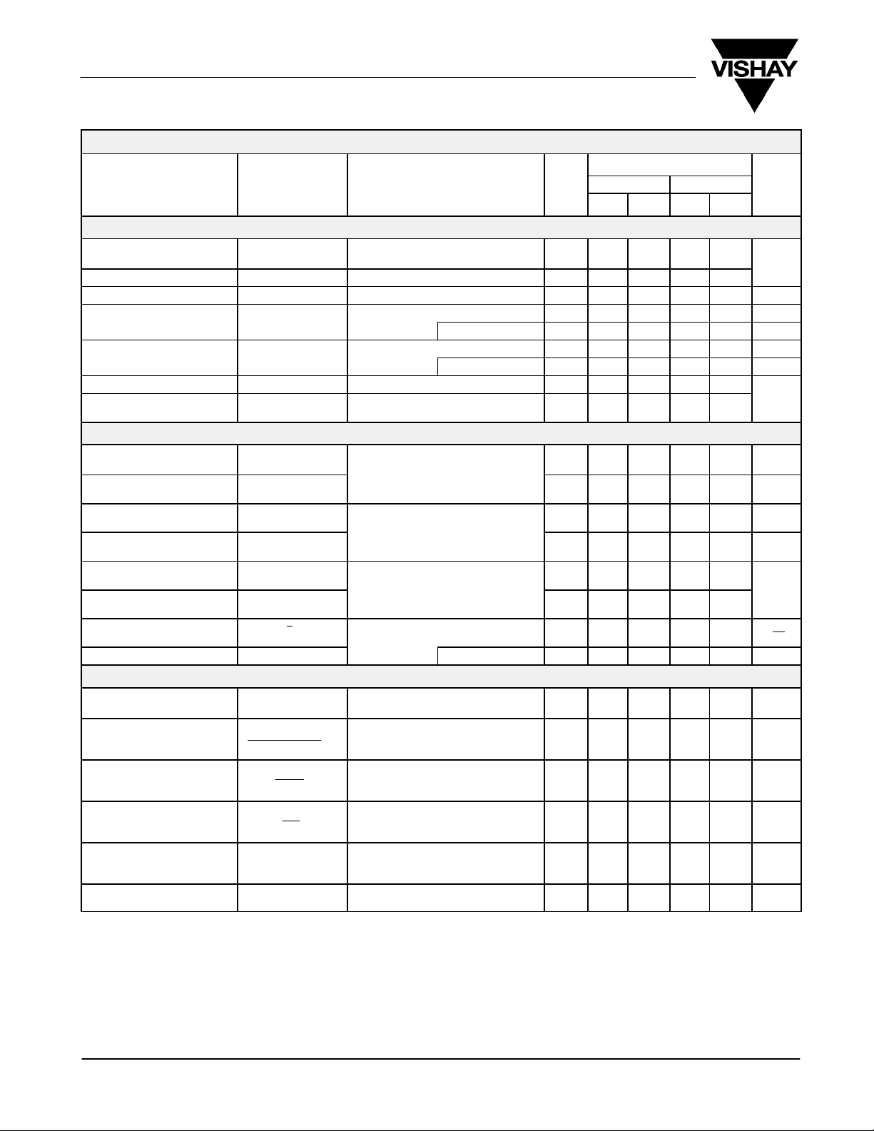
SPECIFICATIONS (TA = 25_C UNLESS OTHERWISE NOTED)
Parameter Symbol Test Conditions TypaMin Max Min Max Unit
Static
Gate-Source
Breakdown Voltage
Gate-Source Cutoff Voltage V
Saturation Drain Current
b
Gate Reverse Current I
Gate Operating Current I
Gate-Source Voltage V
Gate-Source
Forward Voltage
c
Dynamic
Common-Source
Forward Transconductance
Common-Source
Output Conductance
Common-Source
Forward Transconductance
Common-Source
Output Conductance
Common-Source
Input Capacitance
Common-Source Reverse
Transfer Capacitance
Equivalent Input
Noise Voltage
Noise Figure NF
Matching
Differential
Gate-Source Voltage
Gate-Source Voltage
Differential Change
with Temperature
Saturation Drain
Current Ratio
Transconductance Ratio
V
(BR)GSS
GS(off)
I
DSS
IG = –1 mA, VDS = 0 V
VDS = 10 V, ID = 1 nA –3.5 –1 –5 –1 –5
VDS = 10 V, VGS = 0 V 15 7 40 7 40 mA
VGS = –15 V, VDS = 0 V –1 –100 –100 pA
GSS
TA = 150_C
VDG = 10 V, ID = 5 mA –1 –100 –100 pA
V
C
G
GS
GS(F)
g
fs
g
os
g
fs
g
os
C
iss
rss
e
n
VDG = 10 V, IG = 5 mA –1.5 –0.3 –4 –0.3 –4
IG = 1 mA, VDS = 0 V 0.7
VDG = 10 V, ID = 5 mA
VDG = 10 V, ID = 5 mA
VDG = 10 V, ID = 5 mA
VDG = 10 V, ID = 5 mA
f = 100 MHz
VDG = 10 V, ID = 5 mA
VDG = 10 V, ID = 5 mA
VDG = 10 V, ID = 5 mA
TA = 125_C
f = 1 kHz
f = 1 MHz
f = 10 kHz
RG = 100 kW
|
V
GS1
|
D
V
GS1
– V
DT
I
DSS1
I
DSS2
g
g
– V
fs1
fs2
GS2
GS2
|
|
VDG = 10 V, ID = 5 mA 4 10 15 mV
VDG = 10 V, ID = 5 mA
T
= –55 to 125_C
A
VDS = 10 V, VGS = 0 V 0.98 0.95 1 0.95 1
VDS = 10 V, ID = 5 mA
f = 1 kHz
Limits
2N5911 2N5912
–35 –25 –25
–2 –250 –250 nA
–0.3 –100 –100 nA
6 5 10 5 10 mS
70 100 100
5.8 5 10 5 10 mS
90 150 150
3 5 5
1 1.2 1.2
4 20 20
0.1 1 1 dB
15 20 40
0.98 0.95 1 0.95 1
mS
mS
pF
nV⁄
√Hz
mV/_C
V
V
V
|
|
Differential Gate Current
Common Mode
Rejection Ratio
Notes
a. Typical values are for DESIGN AID ONLY, not guaranteed nor subject to production testing. NZF
b. Pulse test: PW v300 ms duty cycle v3%.
c. This parameter not registered with JEDEC.
c
www.vishay.com
8-2
I
G1–IG2
VDG = 10 V, ID = 5 mA, TA = 125_C
0.005 20 20 nA
CMRR VDG = 5 to 10 V, ID = 5 mA 85 dB
Document Number: 70255
S-04031—Rev. D, 04-Jun-01
Page 3
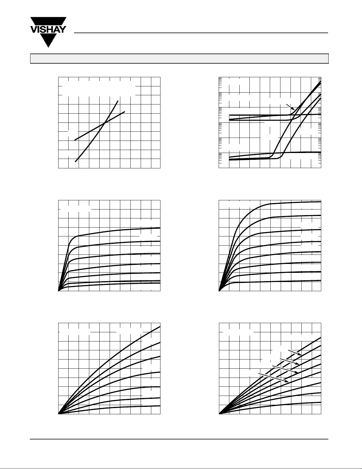
TYPICAL CHARACTERISTICS (TA = 25_C UNLESS OTHERWISE NOTED)
Drain Current and Transconductance
50
40
30
20
– Saturation Drain Current (mA)
10
DSS
I
vs. Gate-Source Cutoff Voltage
I
@ VDS = 10 V, VGS = 0 V
DSS
@ VDS = 10 V, VGS = 0 V
g
fs
f = 1 kHz
g
fs
I
DSS
20
g
fs
– Forward Transconductance (mS)
16
12
8
4
100 nA
10 nA
1 nA
100 pA
– Gate Leakage
G
10 pA
I
1 pA
I
Gate Leakage Current
@ I
G(on)
D
TA = 125_C
I
@ 125_C
GSS
TA = 25_C
2N5911/5912
Vishay Siliconix
ID = 10 mA
1 mA
I
GSS
1 mA
@ 25_C
10 mA
0
0 –10–8–2
–4 –6
V
– Gate-Source Cutoff Voltage (V)
GS(off)
0
0.1 pA
Output Characteristics
10
V
= –2 V
GS(off)
8
6
4
– Drain Current (mA)
D
I
2
0
068210
4
VDS – Drain-Source Voltage (V)
VGS= 0 V
–0.2 V
–0.4 V
–0.6 V
–0.8 V
–1.0 V
–1.2 V
– Drain Current (mA)
D
I
Output Characteristics
5
V
GS(off)
4
3
2
– Drain Current (mA)
D
I
1
= –2 V
VGS= 0 V
–0.2 V
–0.4 V
–0.6 V
–0.8 V
–1.0 V
–1.2 V
– Drain Current (mA)
D
I
0 4 16 20812
VDG – Drain-Gate Voltage (V)
30
V
GS(off)
24
18
12
6
0
08210
15
V
12
9
6
3
Output Characteristics
= –5 V
46
VDS – Drain-Source Voltage (V)
Output Characteristics
= –5 V
GS(off)
–1.0 V
–1.5 V
–2.0 V
VGS= 0 V
–0.5 V
–1.0 V
–1.5 V
–2.0 V
–2.5 V
–3.0 V
–3.5 V
VGS= 0 V
–0.5 V
–2.5 V
–3.0 V
–3.5 V
0
0 0.2 0.8 1
Document Number: 70255
S-04031—Rev. D, 04-Jun-01
0.4 0.6
VDS – Drain-Source Voltage (V)
0
0 0.2 0.8 1
0.4 0.6
VDS – Drain-Source Voltage (V)
www.vishay.com
8-3
Page 4
2N5911/5912
Vishay Siliconix
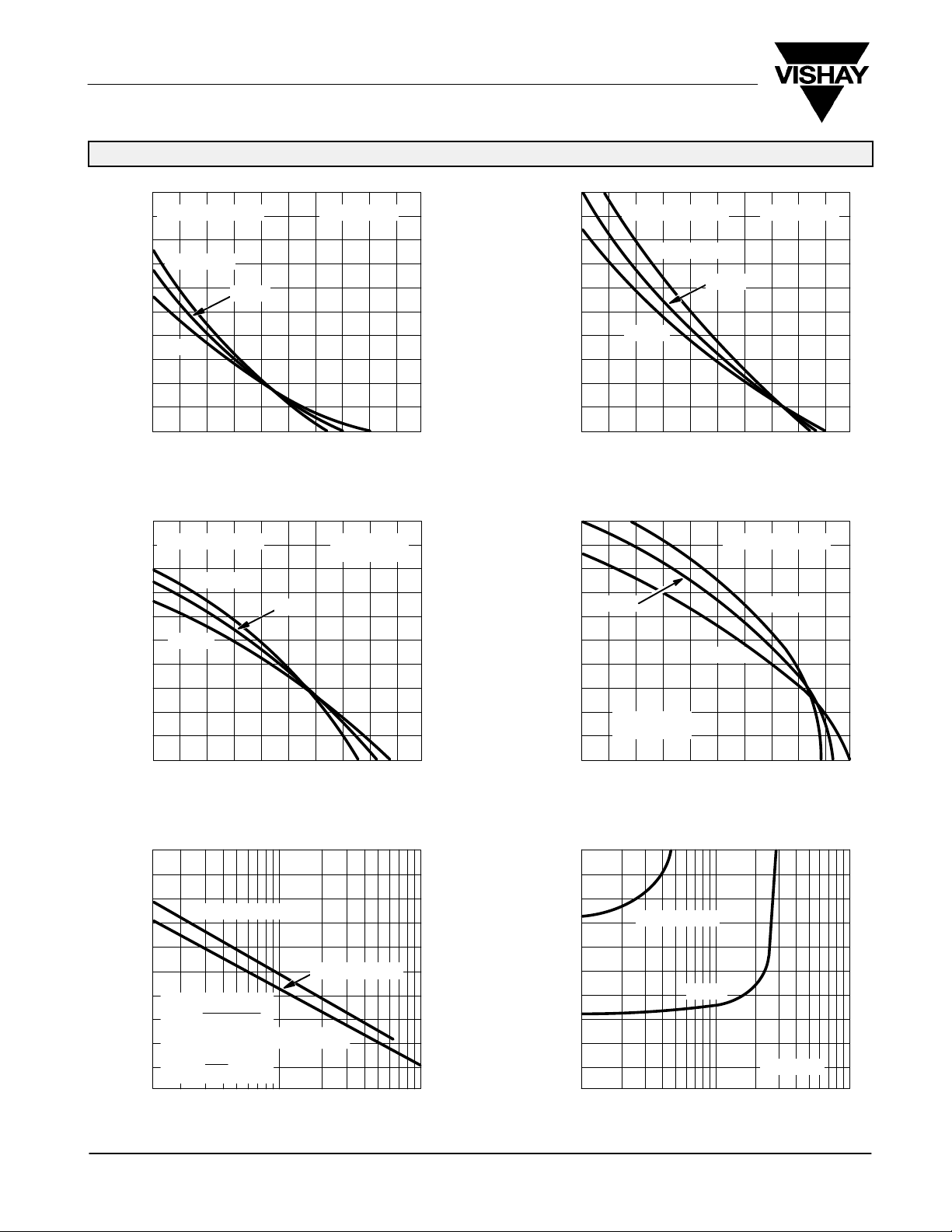
TYPICAL CHARACTERISTICS (TA = 25_C UNLESS OTHERWISE NOTED)
10
V
GS(off)
Transfer Characteristics
30
= –2 V VDS = 10 V V
Transfer Characteristics
GS(off)
= –5 V VDS = 10 V
8
TA = –55_C
6
4
– Drain Current (mA)
D
I
125_C
2
0
0 –0.4 –1.6 –2
Transconductance vs. Gate-Source Voltage
10
V
GS(off)
8
6
4
TA = –55_C
125_C
25_C
–0.8 –1.2
VGS – Gate-Source Voltage (V)
= –2 V V
25_C
f = 1 kHz
24
18
12
– Drain Current (mA)
D
I
6
0
0 –4 –5–1
Transconductance vs. Gate-Source Voltage
10
8
25_C
6
4
TA = –55_C
25_C
125_C
–2 –3
VGS – Gate-Source Voltage (V)
GS(off)
125_C
= –5 VVDS = 10 V
TA = –55_C
2
– Forward Transconductance (mS)
fs
g
0
0 –1.2 –1.6–0.4 –2
Circuit Voltage Gain vs. Drain Current
50
40
30
– Voltage Gain
20
V
A
A
+
V
1 ) RLg
Assume VDD = 15 V, VDS = 5 V
10
0
10 V
R
+
L
–0.8
VGS – Gate-Source Voltage (V)
V
= –2 V
GS(off)
V
GS(off)
g
fsRL
os
I
D
1100.1
I
– Drain Current (mA)
D
= –5 V
2
– Forward Transconductance (mS)
fs
g
0
200
160
120
80
– Drain-Source On-Resistance ( Ω )
40
DS(on)
r
0
VDS = 10 V
f = 1 kHz
–2 –3
VGS – Gate-Source Voltage (V)
On-Resistance vs. Drain Current
V
= –2 V
GS(off)
–5 V
1 10 100
ID – Drain Current (mA)
–5–4–10
TA = 25_C
www.vishay.com
8-4
Document Number: 70255
S-04031—Rev. D, 04-Jun-01
Page 5
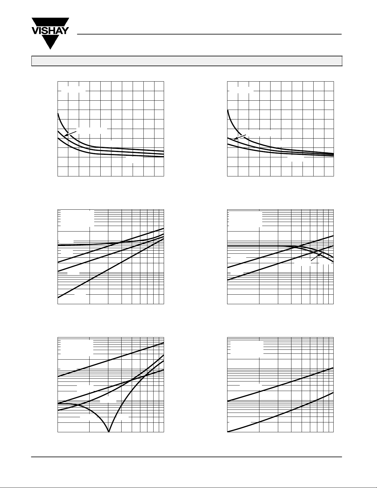
TYPICAL CHARACTERISTICS (TA = 25_C UNLESS OTHERWISE NOTED)
Common-Source Input Capacitance
10
f = 1 MHz
vs. Gate-Source Voltage
Common-Source Reverse Feedback
Capacitance vs. Gate-Source Voltage
5
f = 1 MHz
2N5911/5912
Vishay Siliconix
– Input Capacitance (pF)C
iss
(mS)
8
6
4
2
0
100
10
1
0 –16 –20–4
TA = 25_C
= 10 V
V
DS
= 10 mA
I
D
g
ig
b
is
b
ig
4
3
VDS = 5 V
0 V
10 V
2
1
– Reverse Feedback Capacitance (pF)C
rss
0
–8 –12 –8
V
– Gate-Source Voltage (V)
GS
0 –12 –20–16–4
Input Admittance
100
10
(mS)
1
TA = 25_C
= 10 V
V
DS
= 10 mA
I
D
–b
fs
b
fg
VDS = 5 V
0 V
V
– Gate-Source Voltage (V)
GS
Forward Admittance
10 V
g
–g
fg
fs
g
is
0.1
100 1000
10
TA = 25_C
= 10 V
V
DS
= 10 mA
I
D
–b
rs
1
(mS)
–b
0.1
0.01
100 1000
Document Number: 70255
S-04031—Rev. D, 04-Jun-01
0.1
200 500 200 500
f – Frequency (MHz)
Reverse Admittance
100 1000
f – Frequency (MHz)
100
TA = 25_C
= 10 V
V
DS
= 10 mA
I
D
Output Admittance
10
b
b
og,
rg
–g
rs
–g
rg
g
rg
(mS)
1
g
os
g
og,
os
0.1
200 500 200 500
f – Frequency (MHz)
100 1000
f – Frequency (MHz)
www.vishay.com
8-5
Page 6
2N5911/5912
Vishay Siliconix
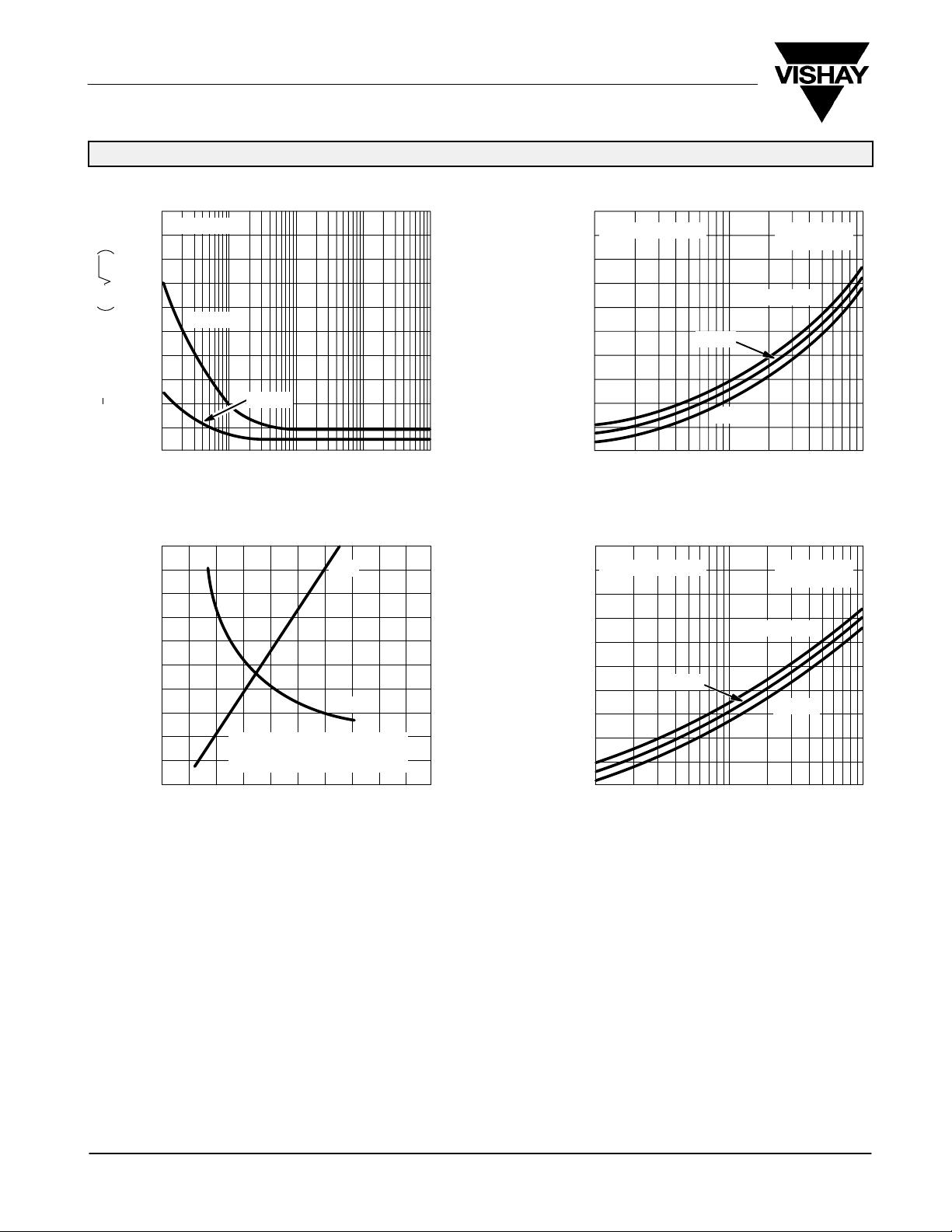
TYPICAL CHARACTERISTICS (TA = 25_C UNLESS OTHERWISE NOTED)
en – Noise Voltage nV/ Hz
Equivalent Input Noise Voltage vs. Frequency
50
VDS = 10 V
40
30
20
10
ID = 1 mA
10 mA
0
10 100 1 k 100 k10 k
f – Frequency (Hz)
On-Resistance and Output Conductance
vs. Gate-Source Cutoff Voltage
200
g
os
160
120
200
160
120
150
120
– Output Conductance (µS)
os
g
Output Conductance vs. Drain Current
V
= –5 V
GS(off)
90
25_C
60
30
0
0.1 1 10
ID – Drain Current (mA)
125_C
VDS = 10 V
f = 1 kHz
TA = –55_C
Common-Source Forward Transconductance
10
V
g
os
– Output Conductance (µS)
GS(off)
8
6
vs. Drain Current
= –5 V
VDS = 10 V
f = 1 kHz
TA = –55_C
80 80
– Drain-Source On-Resistance ( Ω )
40
DS(on)
r
0
0 –10–8–2
rDS @ ID = 1 mA, VGS = 0 V
@ VDS = 10 V, VGS = 0 V
g
os
f = 1 kHz
–4 –6
V
– Gate-Source Cutoff Voltage (V)
GS(off)
r
DS
4
40
0
– Forward Transconductance (mS)
2
fs
g
0
0.1
25_C
125_C
110
ID – Drain Current (mA)
www.vishay.com
8-6
Document Number: 70255
S-04031—Rev. D, 04-Jun-01
Page 7

Legal Disclaimer Notice
Vishay
Disclaimer
All product specifications and data are subject to change without notice.
Vishay Intertechnology, Inc., its affiliates, agents, and employees, and all persons acting on its or their behalf
(collectively, “Vishay”), disclaim any and all liability for any errors, inaccuracies or incompleteness contained herein
or in any other disclosure relating to any product.
Vishay disclaims any and all liability arising out of the use or application of any product described herein or of any
information provided herein to the maximum extent permitted by law. The product specifications do not expand or
otherwise modify Vishay’s terms and conditions of purchase, including but not limited to the warranty expressed
therein, which apply to these products.
No license, express or implied, by estoppel or otherwise, to any intellectual property rights is granted by this
document or by any conduct of Vishay.
The products shown herein are not designed for use in medical, life-saving, or life-sustaining applications unless
otherwise expressly indicated. Customers using or selling Vishay products not expressly indicated for use in such
applications do so entirely at their own risk and agree to fully indemnify Vishay for any damages arising or resulting
from such use or sale. Please contact authorized Vishay personnel to obtain written terms and conditions regarding
products designed for such applications.
Product names and markings noted herein may be trademarks of their respective owners.
Document Number: 91000 www.vishay.com
Revision: 18-Jul-08 1
 Loading...