

Page 1
2N4401
SMALL SIGNAL TRANSISTORS (NPN)
FEATURES
¨ NPN Silicon Epitaxial Planar Transistor
for switching and amplifier applications.
¨ As complementary type, the PNP
transistor 2N4403 is recommended.
¨ On special request, this transistor is
also manufactured in the pin
configuration TO-18.
¨ This transistor is also available in the
SOT-23 case with the type designation
MMBT4401
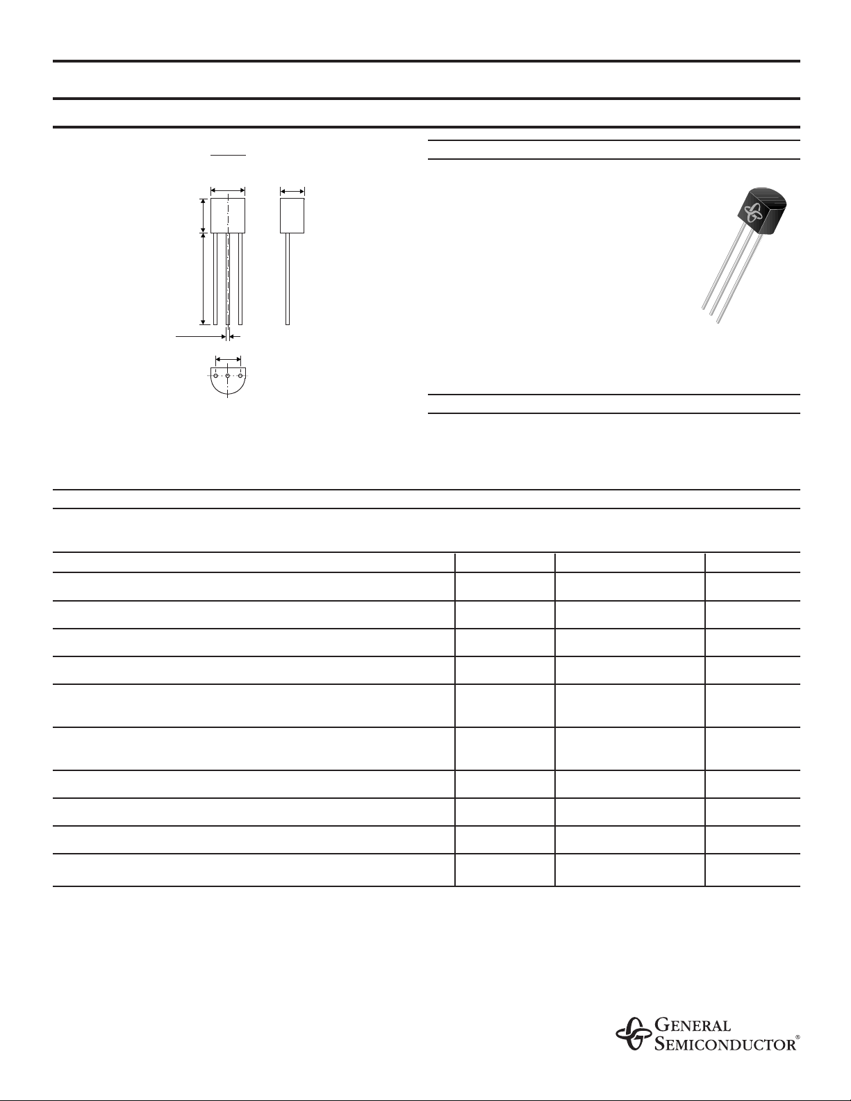
MECHANICAL DATA
Case: TO-92 Plastic Package
Weight: approx. 0.18g
MAXIMUM RATINGS AND THERMAL CHARACTERISTICS
Ratings at 25¡C ambient temperature unless otherwise specified
SYMBOL VALUE UNIT
Collector-Base Voltage V
CBO
60 Volts
Collector-Emitter Voltage V
CEO
40 Volts
Emitter-Base Voltage V
EBO
6.0 Volts
Collector Current-Continuous I
C
600 mA
Power Dissipation at T
A
=25°C
P
tot
625 mW
Derate above 25°C 5.0 mW/°C
Power Dissipation at T
C
=25°C
P
tot
1.5 W
Derate above 25°C 12 mW/°C
Thermal Resistance, Junction to Ambient Air R
QJA
200 °C/W
Thermal Resistance Junction to Case R
QJC
83.3 ¡C/W
Junction Temperature T
j
150 ¡C
Storage Temperature Range T
S
Ð55 to +150 ¡C
0.181 (4.6)
min. 0.492 (12.5)
0.181 (4.6)
0.142 (3.6)
0.098 (2.5)
max.
Æ
0.022 (0.55)
E
C
B
TO-92
2/17/99
Dimensions in inches and (millimeters)
ADVANCED INFORMATION ADVANCED INFORMATION
Page 2
2N4401
ELECTRICAL CHARACTERISTICS
Ratings at 25¡C ambient temperature unless otherwise specified
SYMBOL MIN. MAX. UNIT
Collector-Base Breakdown Voltage
at IC= 0.1 mA, IE = 0
V
(BR)CBO
60 Ð Volts
Collector-Emitter Breakdown Voltage
(1)
at IC = 1 mA, IB = 0
V
(BR)CEO
40 Ð Volts
Emitter-Base Breakdown Voltage
at IE = 0.1 mA, IC = 0
V
(BR)EBO
6.0 Ð Volts
Collector-Emitter Saturation Voltage
(1)
at IC = 150 mA, IB = 15 mA
V
CEsat
Ð 0.40 Volts
at IC = 500 mA, IB = 50 mA
V
CEsat
Ð 0.75 Volts
Base-Emitter Saturation Voltage
(1)
at IC = 150 mA, IB= 15 mA
V
BEsat
0.75 0.95 Volts
at IC = 500 mA, IB= 50 mA
V
BEsat
Ð 1.20 Volts
Collector Cutoff Current
I
CEX
Ð 100 nA
at V
EB
= 0.4 V, V
CE
= 35 V
Base Cutoff Current
at V
EB
= 0.4 V, V
CE
= 35 V
I
BEV
Ð 100 nA
DC Current Gain
at V
CE
= 1 V, IC = 0.1 mA h
FE
20 Ð Ð
at V
CE
= 1 V, IC = 1 mA h
FE
40 Ð Ð
at V
CE
= 1 V, IC = 10 mA h
FE
80 Ð Ð
at V
CE
= 1 V, IC = 150 mA
(1)
h
FE
100 300 Ð
at V
CE
= 2 V, IC = 500 mA
(1)
h
FE
40 Ð Ð
Input Impedance
at V
CE
= 10 V, IC = 1 mA, f = 1 kHz
h
ie
1.0 15 kW
Voltage Feedback Ratio
at V
CE
= 10 V, IC = 1 mA, f = 1 kHz
h
re
0.1 ¥ 10
-4
8 ¥ 10
-4
Ð
Current Gain-Bandwidth Product
at V
CE
= 10 V, IC = 20 mA, f = 100 MHz
f
T
250 Ð MHz
Collector-Base Capacitance
at V
CB
= 5 V, IE=0, f=1.0 MH
Z
C
CBO
Ð 6.5 pF
Emitter-Base Capacitance
at V
EB
= 0.5 V, IC=0, f=1.0 MH
Z
C
EBO
Ð30pF
NOTES
(1) Pulse test: Pulse width ² 300ms - Duty cycle ² 2%
Page 3

2N4401
ELECTRICAL CHARACTERISTICS
Ratings at 25¡C ambient temperature unless otherwise specified
SYMBOL MIN. MAX. UNIT
Small Signal Current Gain
at VCE= 10 V, IC= 1 mA, f = 1 kHz
h
fe
40 500 Ð
Output Admittance
at VCE= 10 V, IC= 1 mA, f = 1 kHz
h
oe
1.0 30 mS
Delay Time (see fig. 1)
at IC= 150 mA, IB1= 15 mA, VCC=30V, VBE=2.0V
t
d
Ð15ns
Rise Time (see fig. 1)
at IC= 150 mA, IB1= 15 mA, VCC=30V, VBE=2.0V
t
r
Ð20ns
Storage Time (see fig. 2)
at IB1= IB2= 15 mA, VCC=30V, IC=150mA
t
s
Ð 225 ns
Fall Time (see fig. 2)
at IB1= IB2= 15 mA, VCC=30V, IC=150mA
t
f
Ð30ns
200W
+30V
-4 V
< 2 ns
0
C * < 10 pF
S
C < 10 pF
S*
200W
1.0 to 100 ms, DUTY CYCLE Å 2% 1.0 to 100 ms, DUTY CYCLE Å 2%
+30V
+16 V
-2 V
1kW 1kW
Scope rise time < 4ns
*Total shunt capacitance of test jig,
connectors and oscilloscope
< 20 ns
0
+16 V
-14 V
SWITCHING TIME EQUIVALENT TEST CIRCUIT
FIGURE 1 - TURN-ON TIME FIGURE 2 - TURN-OFF TIME
 Loading...