

Page 1
GENERAL PURPOSE HIGH-VOLTAGETYPE
DESCRIPTIO N
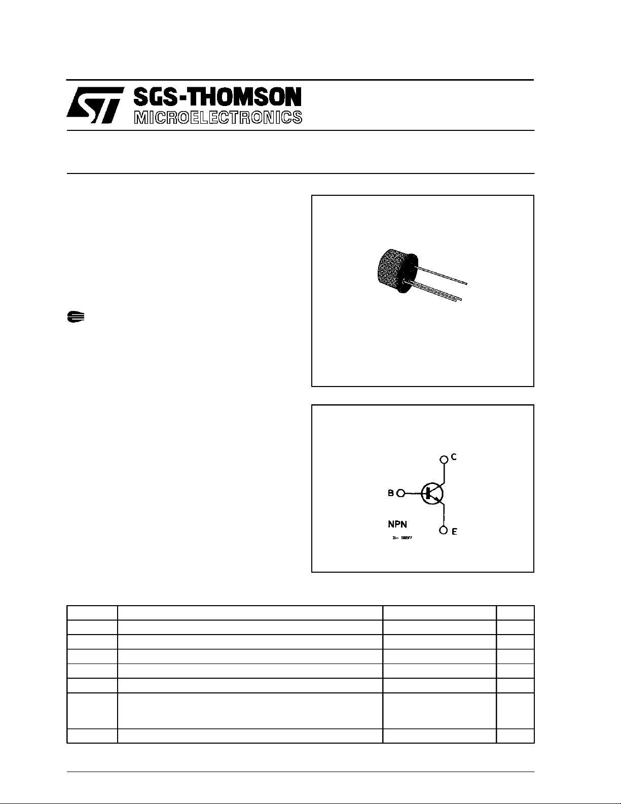
The 2N1893 is a silicon planar epitaxial NPN transistorinJedec TO-39metal case,designed for use
inhigh-performance amplifier,oscillator andswitching circuits.
It provides greater voltage swings in oscillator and
amplifier circuits and more protection in inductive
switchingcircuits due toits 120 V collector-to-base
voltage rating.
Productsapproved to CECC50002-104 available onrequest.
2N1893
TO-39
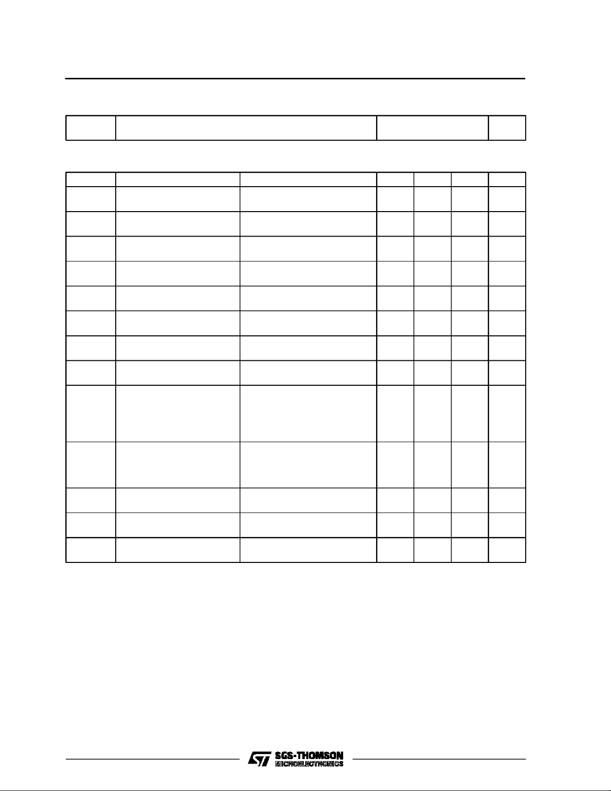
INTERNAL SCHEMATIC DIAGRAM
ABSOLUTE MAXI MUM RATIN G S
Symbol Parameter Value Unit
V
CBO
V
CER
V
CEO
V
EBO
I
C
P
tot
T
stg,Tj
Collector-base Voltage (IE=0) 120 V
Collector-emitter Voltage (RBE≤ 10 Ω)100V
Collector-emitter Voltage (IB=0) 80 V
Emitter-base Voltage (IC=0) 7 V
Collector Current 0.5 A
Total Power Dissipation at T
at T
at T
Storage and Junction Temperature – 65 to 200 °C
amb
case
case
≤ 25 °C
≤ 25 °C
≤ 100 °C
0.8
3
1.7
W
W
W
October 1988
1/5
Page 2
2N1893
THERMAL DATA
R
th j-case
R
th j-amb
ELECTRICAL CHARACTERISTICS (T
Thermal Resistance Junction-case
Thermal Resistance Junction-ambient
amb
Max
Max
=25°C unless otherwise specified)
58
219
Symbol Parameter Test Conditions Min. Typ. Max. Unit
I
CBO
I
EBO
V
(BR) CBO
V
(BR)CER
V
(BR)CEO
V
(BR) EBO
V
CE (s at )
V
BE (sat)
h
FE
h
fe
f
T
C
EBO
C
CBO
* Pulsed : pulse duration = 300 µs, duty cycle = 1 %.
Collector Cutoff Current
(IE=0)
Emitter Cutoff Current
(IC=0)
Collector-base Breakdown
Voltage (IE=0)
* Collector-emitter Breakdown
Voltage (R
BE
≤ 10 Ω)
Collector-emitter Breakdown
Voltage (I
B
=0)
Emitter-base Breakdown
Voltage (IC=0)
* Collector-emitter Saturation
Voltage
* Base-emitter Saturation
Voltage
VCB=90V
VCB=90V T
V
=5V 10 nA
EB
I
=100µA 120 V
C
= 10 mA 100 V
I
C
=10mA 80 V
I
C
=100µA7 V
I
E
IC=50mA
IC=150mA
IC=50mA
IC=150mA
* DC Current Gain IC= 0.1 mA
IC=10mA
I
=150mA
C
IC=10mA
T
=–55°C
amb
Small Signal Current Gain IC=1mA
f = 1 kHz
I
=5mA
C
f = 1 kHz
Transition Frequency IC=50mA
f=20MHz
Emitter-base Capacitance IC=0
f = 1 MHz
Collector-base Capacitance IE=0
f = 1 MHz
10
=150°C
amb
IB=5mA
IB=15mA
IB=5mA
IB=15mA
V
=10V
CE
VCE=10V
V
=10V
CE
20
35
40
0.82
0.96
50
80
80
15
1.2
5
0.9
1.3
120
VCE=10V
20
V
=5V
CE
30
V
=10V
CE
45
V
= 10 V 50 70 MHz
CE
= 0.5 V 55 85 pF
V
EB
V
=10V 13 15 pF
CB
40
70
85
150
°C/W
°C/W
nA
µA
V
V
V
V
2/5
Page 3

DC Current Gain. High-frequency Current Gain.
2N1893
3/5
Page 4

2N1893
TO39 MECHANICAL DATA
DIM.
mm inch
MIN. TYP. MAX. MIN. TYP. MAX.
A 12.7 0.500
B 0.49 0.019
D 6.6 0.260
E 8.5 0.334
F 9.4 0.370
G 5.08 0.200
H 1.2 0.047
I 0.9 0.035
o
L45
(typ.)
4/5
I
H
G
F
L
DA
E
B
P008B
Page 5

2N1893
Information furnished is believed to be accurate and reliable. However, SGS-THOMSON Microelectronics assumes no responsability for the
consequences of use of such information nor forany infringementofpatents or other rights of third parties which may results from its use. No
license isgrantedby implication orotherwiseunder anypatent or patent rights ofSGS-THOMSON Microelectronics.Specificationsmentioned
in this publication are subject to change without notice. This publication supersedes and replaces all information previously supplied.
SGS-THOMSON Microelectronicsproductsare not authorizedforuse as criticalcomponentsinlife supportdevices or systemswithout express
written approval of SGS-THOMSON Microelectonics.
1994 SGS-THOMSON Microelectronics - All Rights Reserved
Australia - Brazil - France - Germany - Hong Kong - Italy - Japan - Korea - Malaysia - Malta - Morocco - The Netherlands -
Singapore - Spain - Sweden - Switzerland - Taiwan - Thailand - UnitedKingdom - U.S.A
SGS-THOMSON MicroelectronicsGROUPOF COMPANIES
5/5
 Loading...