

Page 1

SC28L202
Dual universal asynchronous
receiver/transmitter (DUART)
Objective specification
IC19 Data Handbook
1998 Oct 05
INTEGRATED CIRCUITS
Page 2

Philips Semiconductors Objective specification
SC28L202
Dual universal asynchronous receiver/transmitter
(DUART)
Designed for “Glueless operation in 68XXX and X86 environments”
2
1998 Oct 05
DESCRIPTION
The 28L202 is a high performance functional upgrade for the Philips
dual channel UARTS. The SCC2692 and SC26C92 operating at 3.3
or 5 volts supply with added features and deeper partitioned FIFOs.
Its configuration on power up is similar that of the SC26C92. Its
differences from the SC26C92 are: 256 character receiver, 256
character transmit FIFOs, CRC error detection, 3 and 5 volt
compatibility, 8 I/O ports for each UART. IRDA compatibility,
arbitrating interrupt system and overall faster buss and data speeds.
It is fabricated in an advanced CMOS process that allows stand by
current of less that one microampere.
Pin programming will allow the device to operate with either the
Motorola or Intel bus interface by changing the function of some
pins. (Reset is inverted, DACKN enabled for example).
The Philips Semiconductors 28L202 Dual Universal Asynchronous
Receiver/Transmitter (DUART) is a single-chip CMOS–LSI
communications device that provides two full-duplex asynchronous
receiver/transmitter channels in a single package. It interfaces
directly with microprocessors and may be used in a polled or
interrupt driven system.
The operating mode and data format of each channel can be
programmed independently. Additionally, each receiver and
transmitter can select its operating speed as one of twenty-three
fixed baud rates; a 16X clock derived from a programmable
counter/timer, or an external 1X or 16X clock. The baud rate
generator and counter/timer can operate directly from a crystal or
from external clock inputs. The ability to independently program the
operating speed of the receiver and transmitter make the DUART
particularly attractive for dual-speed channel applications such as
clustered terminal systems.
Each receiver and transmitter is buffered by eight character FIFOs
to minimize the potential of receiver overrun, transmitter underrun
and to reduce interrupt overhead in interrupt driven systems. In
addition, a flow control capability is provided to disable a remote
transmitter when the receiver buffer is full.
Also provided on the 28L202 are a multipurpose 7-bit input port and
a multipurpose 8-bit output port. These can be used as
general-purpose I/O ports or can be assigned specific functions
(such as clock inputs or status/interrupt outputs) under program
control.
The 28L202 are available in two package versions: a 44-pin PLCC
and 44-pin plastic quad flat pack (PQFP).
FEA TURES
•3.3 or 5.0 volt operation
•Dual full-duplex independent asynchronous receiver/transmitters
•256 or larger character FIFOs for each receiver and transmitter
•Power up as 8 bit data no parity one stop bit 9600 baud
•Pin programming (PQFP package) to 68K or 80xxx bus interface
•Programmable data format
– 5 to 8 data bits plus parity
– Odd, even, no parity or force parity
– 1, 1.5 or 2 stop bits programmable in 1/16-bit increments
•16-bit programmable Counter/Timer
•Programmable baud rate for each receiver and transmitter
selectable from:
– 23 fixed rates: 50 to 230.4k baud
– Other baud rates to MHz at 16X
– Programmable user-defined rates derived from a
programmable Counter/timer
– External 1X or 16X clock
•Parity, framing, and overrun error detection
•False start bit detection
•Line break detection and generation
•Programmable channel mode
– Normal (full-duplex)
– Automatic echo
– Local loop back
– Remote loop back
– Multi-drop mode (also called ‘wake-up’ or ‘9-bit’)
•Multi-function 7-bit input port
– Can serve as clock or control inputs
– Change of state detection on eight inputs
– Inputs have typically >100k pull-up resistors
•Multi-function 8-bit output port
– Individual bit set/reset capability
– Outputs can be programmed to be status/interrupt signals
•Versatile interrupt system
– Single interrupt output with eight maskable interrupting
conditions
– Output port can be configured to provide a total of up to six
separate interrupt outputs that may be wire ORed.
– Each FIFO can be programmed for four different interrupt
levels.
– Watch dog timer for each receiver
•Maximum data transfer rates:
– 1X – 1Mb/sec, 16X – 1Mb/sec
•Automatic wake-up mode for multi-drop applications
•Start-end break interrupt/status
•Detects break which originates in the middle of a character
•On-chip crystal oscillator
•Power down mode
•Receiver time-out mode
•Single +3.3V or +5V power supply
•Powers up to emulate SCC2692 and SC26C92
Page 3

Philips Semiconductors Objective specification
SC28L202
Dual universal asynchronous receiver/transmitter
(DUART)
1998 Oct 05
3
ORDERING INFORMATION
ББББББББББББ
Á
ББББББББББББ
Á
DESCRIPTION
БББББББББ
Á
БББББББББ
Á
INDUSTRIAL
V
CC
= +3.3 +5V ±10%,
T
A
= –40 TO +85C
БББББББББ
Á
БББББББББ
Á
DRAWING NUMBER
44-Pin Plastic Leaded Chip Carrier (PLCC)
28L202A1A
SOT187–2
44-Pin Plastic Quad Flat Pack (PQFP)
28L202A1B
SOT307–2
Page 4

Philips Semiconductors Objective specification
SC28L202
Dual universal asynchronous receiver/transmitter
(DUART)
1998 Oct 05
4
PIN CONFIGURATION DIAGRAM
PIN FUNCTION PIN FUNCTION
1NC 27D2
2A0 28D0
3 I/OB3 29 I/OA6
4 A1 30 I/OA4
5 I/OB1 31 I/OA2
6 A2 32 I/OA0
7 A3 33 TxDA
8 I/OB0 34 NC
9 WRN 35 RxDA
10 RDN 36 X1/CLK
11 RxDB 37 X2
12 I/M 38 RESET
13 TxDB 39 CEN
14 I/OA1 40 I/OB2
15 I/OA3 41 I/OB6
16 I/OA5 42 I/OB5
17 I/OA7 43 I/OB4
18 D1 44 V
CC
19 D3 45 A4
20 D5 46 A5
21 D7 47 I/OB7
22 V
SS
48 PRE
23 NC 49 V
CC
24 INTRN 50 V
SS
25 D6 51 NC
26 D4 52 NC
1
46
20
33
47
34
21
8
PLCC
7
TOP VIEW
INDEX
CORNER
SD00680
Page 5

Philips Semiconductors Objective specification
SC28L202
Dual universal asynchronous receiver/transmitter
(DUART)
1998 Oct 05
5
PIN CONFIGURATION DIAGRAM
PIN FUNCTION PIN FUNCTION
1NC 27D2
2A0 28D0
3 I/OB3 29 I/OA6
4 A1 30 I/OA4
5 I/OB1 31 I/OA2
6 A2 32 I/OA0
7 A3 33 TxDA
8 I/OB0 34 NC
9 R/WN 35 RxDA
10 DACKN 36 X1/CLK
11 RxDB 37 X2
12 I/M 38 RESETN
13 TxDB 39 CEN
14 I/OA1 40 I/OB2
15 I/OA3 41 IACKN
16 I/OA5 42 I/OB5
17 I/OA7 43 I/OB4
18 D1 44 V
CC
19 D3 45 A4
20 D5 46 A5
21 D7 47 I/OB7
22 V
SS
48 PRE
23 NC 49 V
CC
24 INTRN 50 V
SS
25 D6 51 NC
26 D4 52 NC
1
46
20
33
47
34
21
8
PLCC
7
TOP VIEW
INDEX
CORNER
SD00681
Page 6
Philips Semiconductors Objective specification
SC28L202
Dual universal asynchronous receiver/transmitter
(DUART)
1998 Oct 05
6
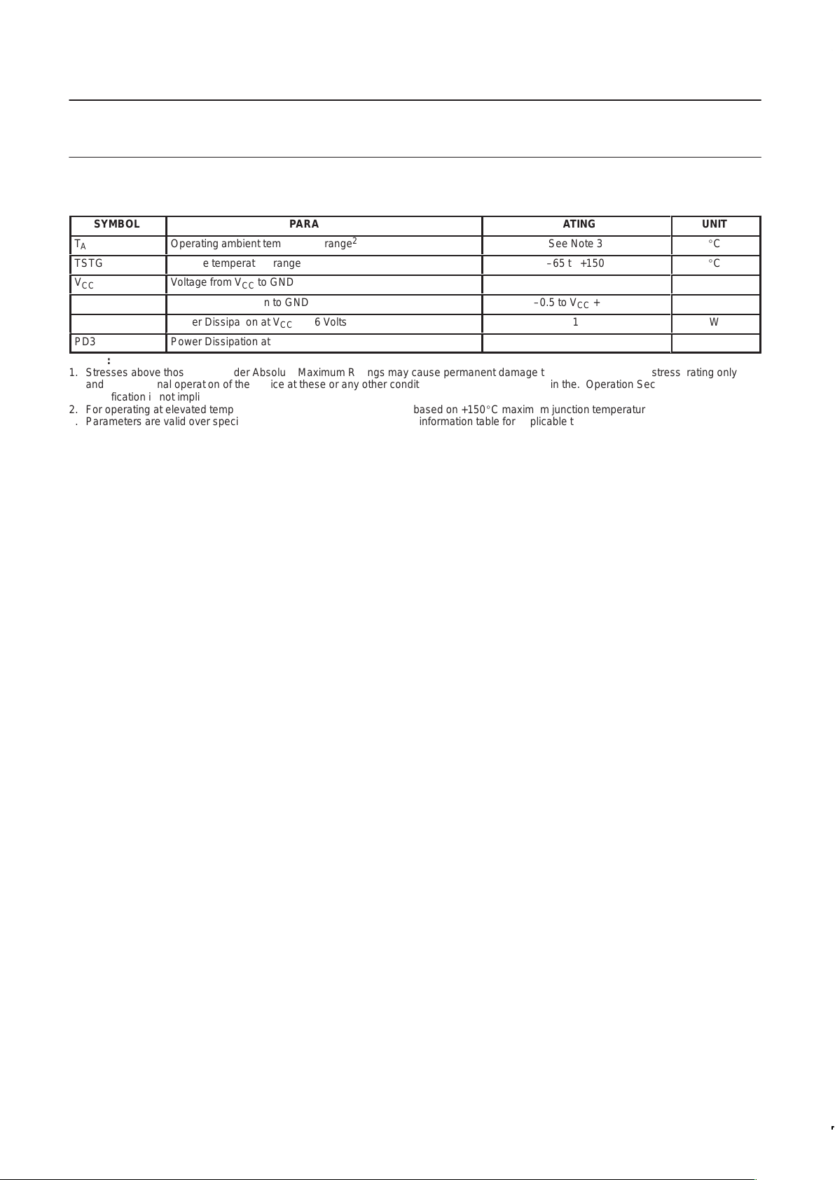
ABSOLUTE MAXIMUM RATINGS
1
SYMBOL
PARAMETER
RATING
БББББ
UNIT
T
A
Operating ambient temperature range
2
See Note 3
БББББ
C
TSTG
Storage temperature range
–65 to +150
БББББ
C
V
CC
Voltage from VCC to GND
4
–0.5 to +7.0
БББББ
V
V
SS
Voltage from any pin to GND
–0.5 to VCC + 0.5
БББББ
V
PD5
Power Dissipation at VCC = 5.6 Volts
1
БББББ
W
PD3
Power Dissipation at VCC = 3.3 Volts
0.5
БББББ
W
NOTES:
1. Stresses above those listed under Absolute Maximum Ratings may cause permanent damage to the device. This is a stress rating only
and the functional operation of the device at these or any other conditions above those indicated in the. Operation Section of this
specification is not implied.
2. For operating at elevated temperatures, the device must be derated based on +150C maximum junction temperature.
3. Parameters are valid over specified temperature range. See ordering information table for applicable temperature range and operating
supply range.
4. This product includes circuitry specifically designed for the protection of its internal devices from damaging effects of excessive static
charge. Nonetheless, it is suggested that conventional precautions be taken to avoid applying any voltages larger than the rated maxim.
Page 7
Philips Semiconductors Objective specification
SC28L202
Dual universal asynchronous receiver/transmitter
(DUART)
1998 Oct 05
7
8
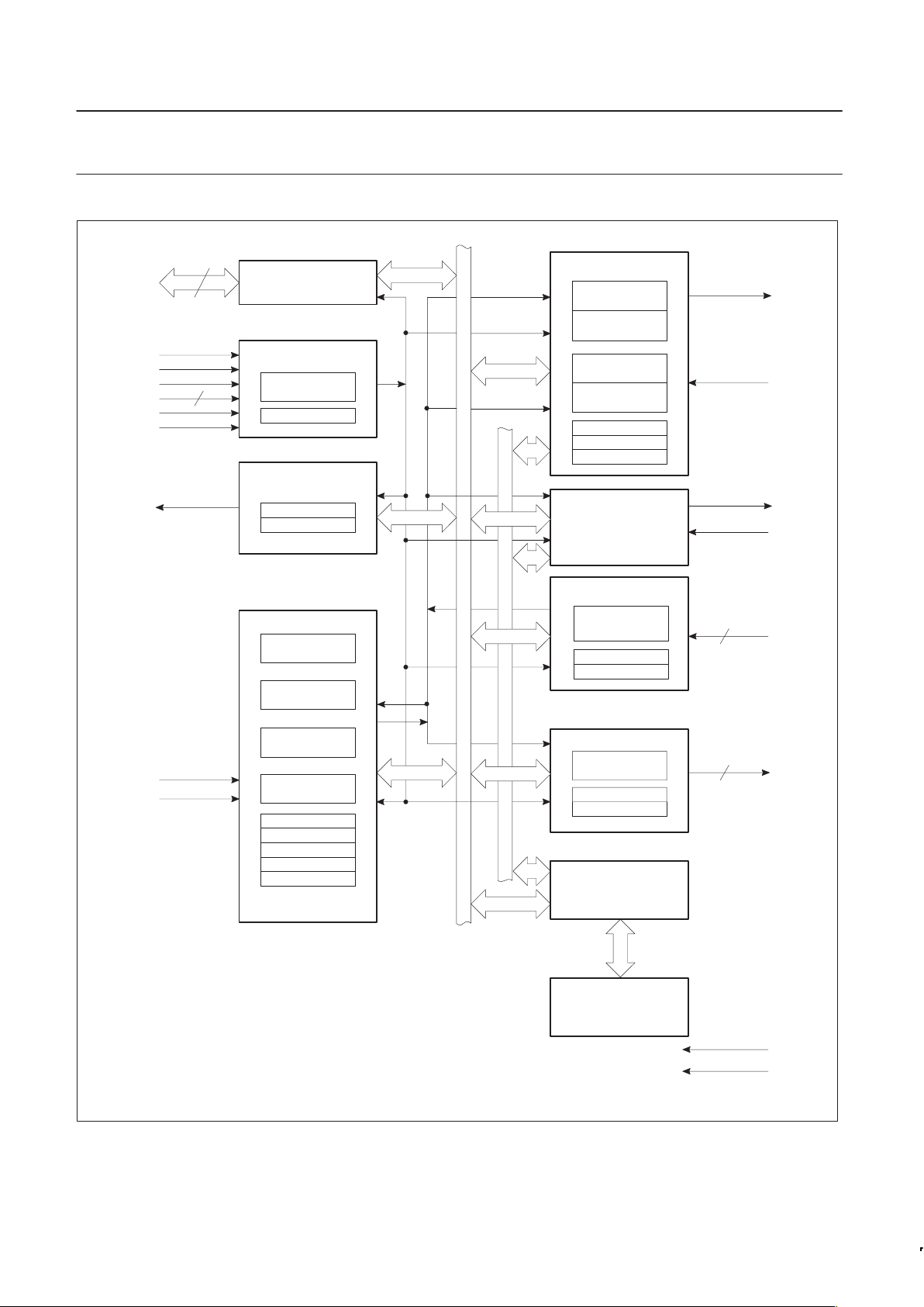
D0–D7
RDN
WRN
CEN
A0–A5
RESET
INTRN
X1/CLK
X2
4
BUS BUFFER
OPERATION CONTROL
ADDRESS
DECODE
R/W CONTROL
INTERRUPT CONTROL
IMR
ISR
TIMING
BAUD RATE
GENERATOR
CLOCK
SELECTORS
COUNTER/
TIMER
XTAL OSC
CSRA
CSRB
ACR
CTLR
CHANNEL A
TRANSMIT
HOLDING REG
TRANSMIT
SHIFT REGISTER
RECEIVE
HOLDING REG (3)
RECEIVE
SHIFT REGISTER
MRA1, 2
CRA
SRA
I/O PORT A
CHANGE OF
STATE
DETECTORS (4)
I/O PORT B
FUNCTION
SELECT LOGIC
OPCR
TxDA
RxDA
I/O7:0A
I/O7:0B
V
CC
GND
CONTROL
TIMING
INTERNAL DATABUS
CHANNEL B
(AS ABOVE)
IPCR
ACR
OPR
CTLR
U
RxDB
TxDB
8
8
SD00679
FIFO
RAM
FIFO DATABUS
FIFO
CONTROL
I/M
Figure 1. Block Diagram
Page 8
Philips Semiconductors Objective specification
SC28L202
Dual universal asynchronous receiver/transmitter
(DUART)
1998 Oct 05
8
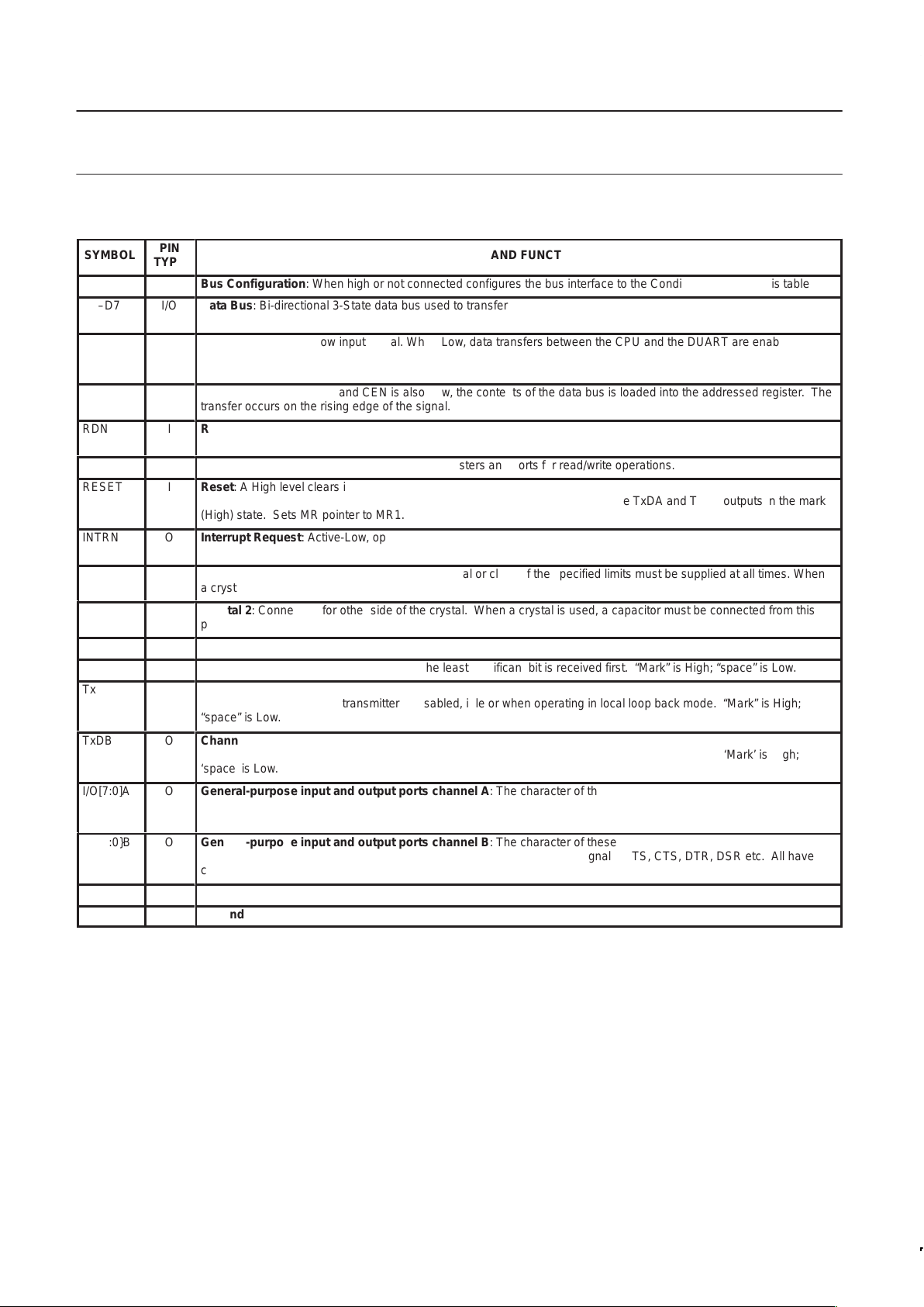
PIN CONFIGURATION FOR 80XXX BUS INTERFACE (INTEL)
ÁÁ
Á
SYMBOL
Á
Á
PIN
TYPE
БББББББББББББББББББББББББББ
Á
NAME AND FUNCTION
I/M
I
Bus Configuration: When high or not connected configures the bus interface to the Conditions shown in this table.
D0–D7
I/O
Data Bus: Bi-directional 3-State data bus used to transfer commands, data and status between the DUART and the
CPU. D0 is the least significant bit.
ÁÁ
Á
ÁÁ
Á
CEN
Á
Á
Á
Á
I
БББББББББББББББББББББББББББ
Á
БББББББББББББББББББББББББББ
Á
Chip Enable: Active-Low input signal. When Low, data transfers between the CPU and the DUART are enabled on
D0–D7 as controlled by the WRN, RDN and A0–A3 inputs. When High, places the D0–D7 lines in the 3-State condition.
WRN
I
Write Strobe: When Low and CEN is also Low, the contents of the data bus is loaded into the addressed register. The
transfer occurs on the rising edge of the signal.
ÁÁ
Á
RDN
Á
Á
I
БББББББББББББББББББББББББББ
Á
Read Strobe: When Low and CEN is also Low, causes the contents of the addressed register to be presented on the
data bus. The read cycle begins on the falling edge of RDN.
A0–A3
I
Address Inputs: Select the DUART internal registers and ports for read/write operations.
ÁÁ
Á
RESET
Á
Á
I
БББББББББББББББББББББББББББ
Á
Reset: A High level clears internal registers (SRA, SRB, IMR, ISR, OPR, OPCR), puts OP0 – OP7 in the High state,
stops the counter/timer, and puts Channels A and B in the inactive state, with the TxDA and TxDB outputs in the mark
(High) state. Sets MR pointer to MR1.
INTRN
O
Interrupt Request: Active-Low, open-drain, output which signals the CPU that one or more of the eight maskable interrupting conditions are true.
ÁÁ
Á
X1/CLK
Á
Á
I
БББББББББББББББББББББББББББ
Á
Crystal 1: Crystal or external clock input. A crystal or clock of the specified limits must be supplied at all times. When
a crystal is used, a capacitor must be connected from this pin to ground (see Figure 7).
ÁÁ
Á
X2
Á
Á
O
БББББББББББББББББББББББББББ
Á
Crystal 2: Connection for other side of the crystal. When a crystal is used, a capacitor must be connected from this
pin to ground (see Figure 7). If X1/CLK is driven from an external source, this pin must be left open.
RxDA
I
Channel A Receiver Serial Data Input: The least significant bit is received first. “Mark” is High; “space” is Low.
RxDB
I
Channel B Receiver Serial Data Input: The least significant bit is received first. “Mark” is High; “space” is Low.
ÁÁ
Á
ÁÁ
Á
TxDA
Á
Á
Á
Á
O
БББББББББББББББББББББББББББ
Á
БББББББББББББББББББББББББББ
Á
Channel A Transmitter Serial Data Output: The least significant bit is transmitted first. This output is held in the
“mark” condition when the transmitter is disabled, idle or when operating in local loop back mode. “Mark” is High;
“space” is Low.
ÁÁ
Á
TxDB
Á
Á
O
БББББББББББББББББББББББББББ
Á
Channel B Transmitter Serial Data Output: The least significant bit is transmitted first. This output is held in the
‘mark’ condition when the transmitter is disabled, idle, or when operating in local loop back mode. ‘Mark’ is High;
‘space’ is Low.
ÁÁ
Á
I/O[7:0]A
Á
Á
O
БББББББББББББББББББББББББББ
Á
General-purpose input and output ports channel A: The character of these pins is controlled by I/OPCR. They may
be inputs or outputs and will present many internal clocks and interrupt signals: RTS, CTS, DTR, DSR etc. All have
change of state detectors and the input is always active.
ÁÁ
Á
I/O[7:0}B
Á
Á
O
БББББББББББББББББББББББББББ
Á
General-purpose input and output ports channel B: The character of these pins is controlled by I/OPCR. They may
be inputs or outputs and will present many internal clocks and interrupt signals: RTS, CTS, DTR, DSR etc. All have
change of state detectors and the input is always active.
V
CC
Pwr
Power Supply: +3.3 or +5V supply input 10%
GND
Pwr
Ground
Page 9
Philips Semiconductors Objective specification
SC28L202
Dual universal asynchronous receiver/transmitter
(DUART)
1998 Oct 05
9
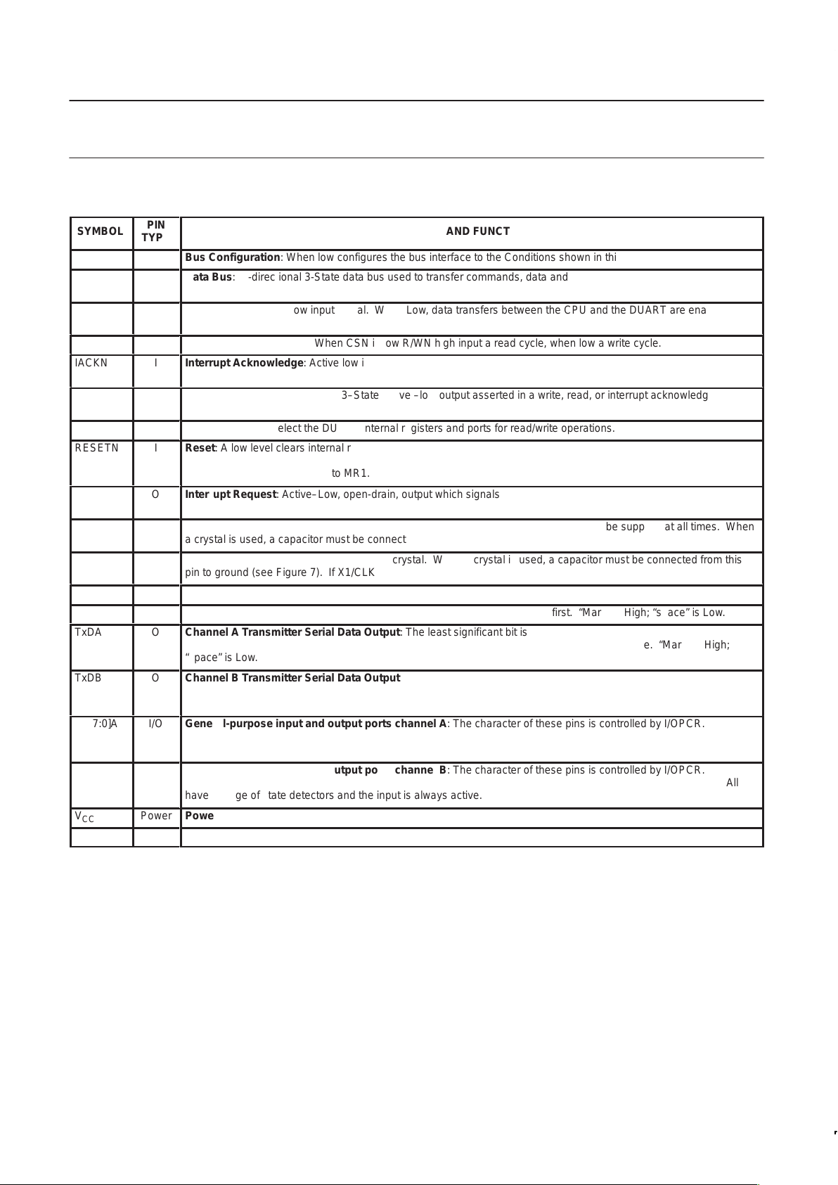
PIN CONFIGURATION FOR 68XXX BUS INTERFACE (INTEL)
ÁÁ
Á
SYMBOL
Á
Á
PIN
TYPE
БББББББББББББББББББББББББББ
Á
NAME AND FUNCTION
I/M
I
Bus Configuration: When low configures the bus interface to the Conditions shown in this table.
D0–D7
I/O
Data Bus: Bi-directional 3-State data bus used to transfer commands, data and status between the DUART and the
CPU. D0 is the least significant bit.
ÁÁ
Á
CSN
Á
Á
I
БББББББББББББББББББББББББББ
Á
Chip Enable: Active-Low input signal. When Low, data transfers between the CPU and the DUART are enabled on
D0–D7 as controlled by the R/WN and A0–A3 inputs. When High, places the D0–D7 lines in the 3-State condition.
R/WN
I
Read/Write: Input Signal. When CSN is low R/WN high input a read cycle, when low a write cycle.
ÁÁ
Á
IACKN
Á
Á
I
БББББББББББББББББББББББББББ
Á
Interrupt Acknowledge: Active low input indicates an interrupt acknowledge cycle. Usually asserted by the CPU in
response to an interrupt request. When asserted places the interrupt vector on the bus and asserts DACKN.
DACKN
O
Data Transfer Acknowledge: A3–State active –low output asserted in a write, read, or interrupt acknowledge cycle to
indicate proper transfer of data between the CPU and the DUART.
A0–A3
I
Address Inputs: Select the DUART internal registers and ports for read/write operations.
ÁÁ
Á
RESETN
Á
Á
I
БББББББББББББББББББББББББББ
Á
Reset: A low level clears internal registers (SRA, SRB, IMR, ISR, OPR, OPCR), puts OP0–OP7 in the High state,
stops the counter/timer, and puts Channels A and B in the inactive state, with the TxDA and TxDB outputs in the mark
(High) state. Sets MR pointer to MR1.
ÁÁ
Á
INTRN
Á
Á
O
БББББББББББББББББББББББББББ
Á
Interrupt Request: Active–Low, open-drain, output which signals the CPU that one or more of the eight maskable
interrupting conditions are true.
X1/CLK
I
Crystal 1: Crystal or external clock input. A crystal or clock of the specified limits must be supplied at all times. When
a crystal is used, a capacitor must be connected from this pin to ground (see Figure 7).
ÁÁ
Á
X2
Á
Á
O
БББББББББББББББББББББББББББ
Á
Crystal 2: Connection for other side of the crystal. When a crystal is used, a capacitor must be connected from this
pin to ground (see Figure 7). If X1/CLK is driven from an external source, this pin must be left open.
RxDA
I
Channel A Receiver Serial Data Input: The least significant bit is received first. “Mark” is High; “space” is Low.
RxDB
I
Channel B Receiver Serial Data Input: The least significant bit is received first. “Mark” is High; “space” is Low.
ÁÁ
Á
TxDA
Á
Á
O
БББББББББББББББББББББББББББ
Á
Channel A Transmitter Serial Data Output: The least significant bit is transmitted first. This output is held in the
“mark” condition when the transmitter is disabled, idle or when operating in local loop back mode. “Mark” is High;
“space” is Low.
ÁÁ
Á
TxDB
Á
Á
O
БББББББББББББББББББББББББББ
Á
Channel B Transmitter Serial Data Output: The least significant bit is transmitted first. This output is held in the
‘mark’ condition when the transmitter is disabled, idle, or when operating in local loop back mode. ‘Mark’ is High;
‘space’ is Low.
ÁÁ
Á
I/O[7:0]A
Á
Á
I/O
БББББББББББББББББББББББББББ
Á
General-purpose input and output ports channel A: The character of these pins is controlled by I/OPCR. They
may be inputs or outputs and will present many internal clocks and interrupt signals: RTS, CTS, DTR, DSR etc. All
have change of state detectors and the input is always active.
ÁÁ
Á
ÁÁ
Á
I/O[7:0]B
Á
Á
Á
Á
I/O
БББББББББББББББББББББББББББ
Á
БББББББББББББББББББББББББББ
Á
General-purpose input and output ports channel B: The character of these pins is controlled by I/OPCR. They
may be inputs or outputs and will present many internal clocks and interrupt signals: RTS, CTS, DTR, DSR etc. All
have change of state detectors and the input is always active.
V
CC
Power
Power Supply: +3.3 or +5V supply input 10%
V
SS
Power
Ground
Page 10
Philips Semiconductors Objective specification
SC28L202
Dual universal asynchronous receiver/transmitter
(DUART)
1998 Oct 05
10
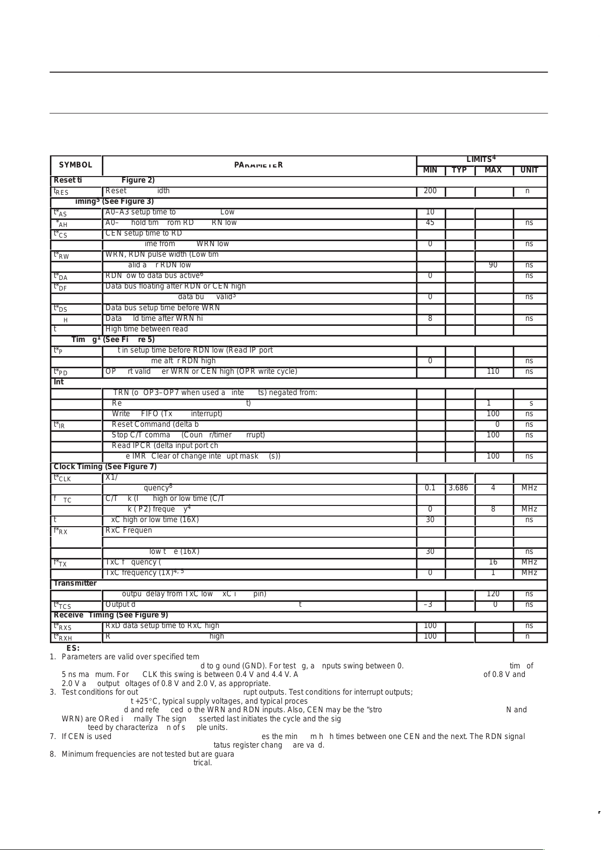
AC CHARACTERISTICS
1, 2, 3
LIMITS
4
SYMBOL
PARAMETER
MIN
TYP
MAX
ÁÁÁ
UNIT
Reset timing (See Figure 2)
t
RES
Reset Pulse Width
200
ÁÁÁ
ns
Bus Timing5 (See Figure 3)
t*
AS
A0–A3 setup time to RDN, WRN Low
10
ÁÁÁ
ns
t*
AH
A0–A3 hold time from RDN, WRN low
45
ns
t*
CS
CEN setup time to RDN, WRN low
0
ÁÁÁ
ns
t*
CH
CEN Hold time from RDN WRN low
0
ÁÁÁ
ns
t*
RW
WRN, RDN pulse width (Low time)
110
ns
t*
DD
Data valid after RDN low
90
ÁÁÁ
ns
t*
DA
RDN low to data bus active
6
0
ÁÁÁ
ns
t*
DF
Data bus floating after RDN or CEN high
30
ÁÁÁ
ns
t*
DI
RDN or CEN high to data bus invalid
3
0
ns
t*
DS
Data bus setup time before WRN or CEN high (write cycle)
75
ÁÁÁ
ns
t*
DH
Data hold time after WRN high
8
ÁÁÁ
ns
t*
RWD
High time between read and/or write cycles
1, 7
55
ns
Port Timing1 (See Figure 5)
t*
PS
Port in setup time before RDN low (Read IP ports cycle)
0
ÁÁÁ
ns
t*
PH
Port in hold time after RDN high
0
ns
t*
PD
OP port valid after WRN or CEN high (OPR write cycle)
110
ÁÁÁ
ns
Interrupt Timing (See Figure 6)
INTRN (or OP3–OP7 when used as interrupts) negated from:
ÁÁÁ
Read RxFIFO (RxRDY/FFULL interrupt)
100
ns
Write TxFIFO (TxRDY interrupt)
100
ÁÁÁ
ns
t*
IR
Reset Command (delta break change interrupt)
100
ÁÁÁ
ns
Stop C/T command (Counter/timer interrupt)
100
ns
Read IPCR (delta input port change interrupt)
100
ÁÁÁ
ns
Write IMR (Clear of change interrupt mask bit(s))
100
ÁÁÁ
ns
Clock Timing (See Figure 7)
t*
CLK
X1/CLK high or low time
80
ÁÁÁ
ns
f*
CLK
X1/CLK frequency
8
0.1
3.686
4
ÁÁÁ
MHz
f*
CTC
C/T Clk (IP2) high or low time (C/T external clock input)
55
ÁÁÁ
ns
f*
CTC
C/T Clk (IP2) frequency
4
0
8
MHz
t*
RX
RxC high or low time (16X)
30
ÁÁÁ
ns
f*
RX
RxC Frequency (16X)
0
16
ÁÁÁ
MHz
RxC Frequency (1x)
4, 9
0
1
MHz
t*
TX
TxC High or low time (16X)
30
ÁÁÁ
ns
f*
TX
TxC frequency (16X)
16
ÁÁÁ
MHz
TxC frequency (1X)
4, 5
0
1
ÁÁÁ
MHz
Transmitter Timing (See Figure 8)
t*
TXD
TxD output delay from TxC low (TxC input pin)
120
ÁÁÁ
ns
t*
TCS
Output delay from TxC output pin low to TxD data output
–30
30
ÁÁÁ
ns
Receiver Timing (See Figure 9)
t*
RXS
RxD data setup time to RxC high
100
ÁÁÁ
ns
t*
RXH
RxD data hold time from RxC high
100
ÁÁÁ
ns
NOTES:
1. Parameters are valid over specified temperature range.
2. All voltage measurements are referenced to ground (GND). For testing, all inputs swing between 0.4 V and 3.0 V with a transition time of
5 ns maximum. For X1/CLK this swing is between 0.4 V and 4.4 V . All time measurements are referenced at input voltage of 0.8 V and
2.0 V and output voltages of 0.8 V and 2.0 V , as appropriate.
3. Test conditions for outputs; C
L
= 150 pF, except interrupt outputs. Test conditions for interrupt outputs; CL = 50 pF, RL = 2.7 Kohm to VCC.
4. Typical values are at +25C, typical supply voltages, and typical processing parameters.
5. Timing is illustrated and referenced to the WRN and RDN inputs. Also, CEN may be the “strobing” input. CEN and RDN (also CEN and
WRN) are ORed internally. The signal asserted last initiates the cycle and the signal negated first terminates the cycle.
6. Guaranteed by characterization of sample units.
7. If CEN is used as the “strobing” input, the parameter defines the minimum high times between one CEN and the next. The RDN signal must
be negated for t
RWD
to guarantee that any status register changes are valid.
8. Minimum frequencies are not tested but are guaranteed by design.
9. Clocks for 1X mode should be symmetrical.
Page 11

Philips Semiconductors Objective specification
SC28L202
Dual universal asynchronous receiver/transmitter
(DUART)
1998 Oct 05
11
OVER ALL DESCRIPTION
The SC28L202 is composed of several functional blocks. They are
listed in the approximate order of hierarchy as seen from the pins of
the device.
•Timing Circuits
•Bus interface. 68K or x86 format
•I/O Ports
•UARTS
•Arbitrating Interrupt Structure
•Character & Address Recognition
•Variable FIFO Partition Structure
•Test Modes and Boundary Scan
BRIEF DESCRIPTION OF FUNCTIONAL BLOCKS
Timing Circuits
Crystal Oscillator
The crystal oscillator is the main timing element for the 28L202. It is
nominally set at 14.7456 MHz and may be used to 29.4912 MHz.
The use of an external clock allows all frequencies to 40 MHz.
BRG
The BRG is the baud rate generator, is driven by the crystal input
and generated all of the 24 “fixed” internal baud rates.
Counter-Timer .
The counter-timer provides miscellaneous baud rated, timing
periods and acts as an extra watchdog timer for the for the
receivers. It has 8 clock sources.
Bus Interface
The bus interface operates in “68K” or “x86” format as selected by
the I/M pin. The signals used by this section are the Address, Data
bus, Chip select, read/write, Data acknowledge and Interrupt
acknowledge and Interrupt request. Assertion of DACKN requires
two edges of the X1clk after the assertion of CEN.
I/O ports
Each UART is provided with 8 I/O ports. Each port is equipped with
a change of state detector. The input circuit of these pins is always
active. Under program control the ports my display internal signals
or static logic levels. The functions represented by the I/O ports
include hardware flow control. Modem signals, signals for interrupt
conditions or various internal clocks and timing intervals. Noisy
inputs to the I/O ports are filtered (de-bounced) by a 38.4 KHz clock.
UARTS
The uarts are fully independent, full duplex and provide all normal
asynchronous functions: 5 to 8 data bits, parity odd or even,
programmable stop bit length, false start bit detection. Also
provided are 256 byte FIFOs Xon/Xoff software flow control and
IRDA pulse modulation. The BRG, Counter-timer, or external clocks
provide the baud rates. The receivers and transmitters may operate
in either the “1x” or “16x” modes.
Interrupt Arbitration
The interrupt system uses a highly programmable arbitrating
technique to establish when an interrupt should be presented to the
processor. The advantageous feature of this system is the
presentation of the context of the interrupt. It is presented in both a
current interrupt register and in the interrupt vector. The context of
the interrupt shows the interrupting channel, identifies which of the 8
possible sources in requesting interrupt service and in the case of a
receiver or transmitter gives the current fill level of the FIFO.
The content of the current interrupt register also drives the Global
Registers of the interrupt system. These registers are indirect
addresses (pointers) to the fields describing the internal source
requesting interrupt service.
Programming of Bid Control Registers allows the interrupt level of
any source to be varied at any time over a range of 256 levels.
Character and Address Recognition
The character recognition system is designed as a general system.
There is one for each UART. Each recognition block stores up to
three characters. The recognition is done on a byte boundary and
sets status and interrupt when an recognition event occurs. Each
has four modes of operation.
A subset of the recognition system is Xon/Xoff character recognition
and multi-drop address recognition. If Xon/Xoff or multi-dorp
function is enabled the recognition system passes the information
about the recognition event to the appropriate receiver or transmitter
state machine for execution. In any case the information about a
recognition event is available to the interrupt system and to the
control processor.
FIFO Partitioning and Control
The FIFO memory is implemented in ram. Nominally 1000 bytes of
ram are divided between the four FIFOs of the DUART. The default
partition is 256 (0xFF) bytes for each fifo. Under program control
size of the partition for any a particular FIFO may be varied from 1 to
1024.
The interrupt level for each FIFO is also under program control and
is continuously variable through out the range of the partition. A
small processor controls all of the FIFO reading, writing, interrupting,
flow control signaling, and status reporting.
Test Modes
Three test modes are provided to verify UART function and
processor interface integrity . These are Auto echo, Local Loop
Back, and Remote Loop Back. Through local loop back the
software developer may verify all of the interrupt, flow control; the
hardware designer verifies all of the timing and pin connections. This
information is obtained without any recourse to external test
equipment or terminals.
Boundary scan provides verification of manufacturing process and
to a lesser extent identifies damage that may occur to pins due to
electrical over stress or electrostatic discharge.
DET AILED DESCRIPTIONS
NOTE: For the convenience of the reader some paragraphs in the
following section will be repeated in descriptions of closely linked
functions.
Timing Circuits
Crystal Oscillator
The crystal oscillator operates directly from a crystal, tuned between
14.7456 MHz and 29 4912 MHz connected across the X1/CCLK and
X2 inputs with a minimum of external components. BRG values
listed for the clock select registers correspond to a 14.7456 MHz
Page 12

Philips Semiconductors Objective specification
SC28L202
Dual universal asynchronous receiver/transmitter
(DUART)
1998 Oct 05
12
crystal frequency. Use of different frequencies will change the
“standard” baud rates by precisely the ratio of 14.7456 to the
different crystal.
An external clock up to 40 MHz frequency range may be connected
to X1/CCLK. If an external clock is used instead of a crystal,
X1/CCLK must be driven and X2 left floating. The X1 clock serves
as the basic timing reference for the baud rate generator (BRG) and
is available to the BRG timers, counter-timers, and control logic.
Baud Rate Generator BRG
The baud rate generator operates from the oscillator or external
X1/CCLK clock input and generates 24 commonly used data
communications baud rates (including MIDDI) ranging from 50 to
230.4K baud. These common rates may be doubled (up to 460.8
and 1500K baud) when faster clocks are used on the X1/X2 clock
inputs. (See Receiver and Transmitter Clock Select Register
descriptions.) All of these are available simultaneously for use by
any receiver or transmitter. The clock outputs from the BRG are at
16X the actual baud rate.
Counter-Timer
The two Counter/Timers are programmable 16 bit dividers that are
used for generating miscellaneous clocks or generating timeout
periods. These clocks may be used by any or all of the receivers
and transmitters in the DUART or may be directed to an I/O pin for
external use.
Counter/Timer programming
The counter timer is a 16-bit programmable divider that operates in
one of five modes: character count, pulse mode, counter, timer, and
time out. Character count counts characters. The pulse mode
generates a periodic pulse of one clock period in width. The timer
mode it generates a square wave. In the counter mode it generates
a time delay. In the time out mode it monitors the time between
received characters. The C/T uses the numbers loaded into the
Counter/Timer Lower Register (CTLR) and the Counter/T imer Upper
Register (CTUR) as its divisor. The counter timer is controlled with
six commands: Start/Stop C/T, Read/Write Counter/Timer lower
register and Read/Write Counter/Timer upper register. These
commands have slight differences depending on the mode of
operation. Please see the detail of the commands under the
CTLR/CTUR Register descriptions.
When ever the these timers are selected via the receiver or
transmitter Clock Select register their output will be configured as a
16x clock for the respective receiver or transmitter. Therefore one
needs to program the timers to generate a clock 16 times faster than
the data rate. The formula for calculating ’n’, the number loaded to
the CTUR and CTLT registers.
For the timer mode the formula is as follows:
n
Brg timer input frequency
2 16 Baud rate desired
–1
For the pulse mode the formula is as follows:
n
Brg timer input frequency
16 Baud rate desired
–1
Note: ‘n’ may assume values of 0 and 1. In previous Philips data
communications controllers these values were not allowed. The
counter/timer control register (CTCR) controls the BRG timer input
frequency.
The frequency generated from the above formula will be at a rate 16
times faster than the desired baud rate. The transmitter and
receiver state machines include divide by 16 circuits, which provide
the final frequency and provide various timing edges used in the
qualifying the serial data bit stream. Often this division will result in
a non-integer value: 26.3 for example. One may only program
integer numbers to a digital divider . There for 26 would be chosen.
If 26.7 were the result of the division then 27 would be chosen. This
gives a baud rate error of 0.3/26.3 or 0.3/26.7 that yields a
percentage error of 1.14% or 1.12% respectively, well within the
ability of the asynchronous mode of operation. Higher input
frequency to the counter reduces the error effect of the fractional
division.
One should be cautious about the assumed benign effects of small
errors since the other receiver or transmitter with which one is
communicating may also have a small error in the precise baud rate.
In a “clean” communications environment using one start bit, eight
data bits and one stop bit the total difference allowed between the
transmitter and receiver frequency is approximately 4.6%. Less
than eight data bits will increase this percentage.
Bus Interface
The bus interface operates in two modes selected by the I/M pin. If
this pin is high or left open the signals DACKN signal is not
generated or used and data flow to and from the chip is controlled
by the state the CEN, RDN, WRN pin combination. If the I/M pin is
tied low the data is written to the device when the DACKN pin is
asserted low by the DUART. Read data is presented by a delay from
CEN active.
The Host interface is comprised of the signal pins CEN, WRN RDN,
(or R/WN) IACKN, DACKN, IRQN, 6 address pins and 8 three-state
data bus pins.
Addressing of the various functions of the DUART is through the
address bus A (5:0). Data is presented on the 8-bit data bus.
DACKN Cycle
When operating in the “68K” mode bus cycle completion is indicated
by the DACKN pin (an open drain signal) going low. This occurs two
X1 clock edges after the cycle begins. Usually in this mode the
address and data are set up with respect to the leading edges of the
bus cycle.
When operating in the “x86” mode DACKN is not generated. Data is
written on the termination of CEN or WRN which ever one occurs
first. Read data is presented from the leading edge of the read
condition; CEN and RDN both low.
IACKN Cycle, Update CIR
When the host CPU responds to the interrupt, it will usually assert
the IACKN signal low. This will cause the DUART to generate an
IACKN cycle in which the condition of the interrupting device is
determined. When IACKN asserts, the last valid interrupt number is
captured in the CIR. The value captured presents all of the
important details of the highest priority interrupt at the moment the
IACKN (or the “Update CIR” command) was asserted. Due to
system interrupt latency, the interrupt condition captured by the CIR
may not be the condition that caused the initial assertion of the
interrupt.
The Dual UART will respond to the IACKN cycle with an interrupt
vector. The interrupt vector may be a fixed value, the content of the
Interrupt Vector Register, or when “Interrupt Vector Modification” is
enabled via ICR, it may contain codes for the interrupt type and/or
Page 13

Philips Semiconductors Objective specification
SC28L202
Dual universal asynchronous receiver/transmitter
(DUART)
1998 Oct 05
13
interrupting channel. This allows the interrupt vector to steer the
interrupt service directly to the proper service routine. The interrupt
value captured in the CIR remains until another IACKN cycle occurs
or until an “Update CIR” command is given to the DUART. The
interrupting channel and interrupt type fields of the CIR set the
current “interrupt context” of the DUART. The channel component of
the interrupt context allows the use of Global Interrupt Information
registers that appear at fixed positions in the register address map.
For example, a read of the Global RxFIFO will read the channel B
RxFIFO if the CIR interrupt context is channel B receiver. At
another time read of the GRxFIFO may read the channel A RxFIFO
(CIR holds a channel A receiver interrupt) and so on. Global
registers exist to facilitate qualifying the interrupt parameters and for
writing to and reading from FIFOs without explicitly addressing them.
The CIR will load with 0x’00 if IACKN or Update CIR is asserted
when the arbitration circuit is NOT asserting an interrupt. In this
condition there is no arbitration value that exceeds the threshold
value. When Interrupt vector modification is active in this situation
the interrupt vector bits associated with the CIR will all be zero.
I/O Ports
Eight I/O ports are provided for each channel. They may be
programmed to be inputs or outputs. The input circuits are always
active whether programmed as and input or an output. A 2 bit code
controls what function these pins will present. Most I/O ports default
to high impedance input state on power up. Those pins used for
modem control (RTS, DTR) will set to output high unless the PRE
pin is tied low.
Input Characteristics
Eight I/O pins are provided for each channel. These pins are
configured individually to be inputs or outputs. As inputs they may
be used to bring external data to the bus, as clocks for internal
functions or external control signals. Each I/O pin has a “Change of
State” detector. The change detectors are used to signal a change
in the signal level at the pin (Either 0 to 1 or 1 to 0 transitions). The
level change on these pins must be stable for 25 to 50 us (two
edges of the 38.4 KHz baud rate clock) before the detectors will
signal a valid change. These are typically used for interface signals
from modems to the DUART and from there to the host.
Output Port
The OPR, OPCR, MR, and CR registers may control the I/O pins
when configured as outputs. Via appropriate programming the pins
of the output port may be configures as another parallel port to
external circuits, or they may represent internal conditions of the
UART. When this 8-bit port is used as a general-purpose output
port, the output port pins drive a state that is the complement of the
Output Port Register (OPR). The OPR register is set and reset by
writing to the SOPR and ROPR addresses. (See the description of
the SOPR and ROPR registers). The output pins will drive the
inverse data polarity of the OPR registers. The OPCR register
conditions these output pins to be controlled by the OPR or by other
signals in the chip. Output ports are driven high on hardware reset.
UART Operation
Receiver and Transmitter
The Dual UART has two full duplex asynchronous
receiver/transmitters. The operating frequency for the receiver and
transmitter can be selected independently from the baud rate
generator, the counter, or from an external input. Registers that are
central to basic full-duplex operation are the mode registers (MR0,
MR1 and MR2), the clock select registers (RxCSR and TxCSR), the
command register (CR), the status register (SR), the transmit
holding register (TxFIFO), the receive holding register (RxFIFO)
interrupt status register (ISR) and interrupt mask register (IMR).
Transmitter Status Bits
The SR (Status Register, one per UART) contains two bits that show
the condition of the transmitter FIFO. These bits are TxRDY and
TxEMT. TxRDY means the TxFIFO has space available for one or
more bytes; TxEMT means The TxFIFO is completely empty and
the last stop bit has been completed. TxEMT can not be active
without TxRDY also being active. These two bits will go active upon
initial enabling of the transmitter. They will extinguish on the disable
or reset of the transmitter.
Transmission resumes and the TxEMT bit is cleared when the CPU
loads at least one new character into the TxFIFO. The TxRDY will
not extinguish until the TxFIFO is completely full. The TxRDY bit will
always be active when the transmitter is enabled and there is at
lease one open position in the TxFIFO.
The transmitter is disabled by a hardware reset, a transmitter reset
in the command register or by the transmitter disable bit also in the
command register (CR). The transmitter must be explicitly enabled
via the CR before transmission can begin. Note that characters
cannot be loaded into the TxFIFO while the transmitter is disabled,
hence it is necessary to enable the transmitter and then load the
TxFIFO. It is not possible to load the TxFIFO and then enable the
transmission.
Note the difference between transmitter disable and transmitter
reset.
Either hardware or software may cause the reset action. When
reset the transmitter stops transmission immediately. The transmit
data output will be driven high, transmitter status bits set to zero and
any data remaining in the TxFIFO will be discarded.
The transmitter disable is controlled by the Tx Enable bit in the
command register. Setting this bit to zero will not stop the
transmitter immediately but will allow it to complete any tasks
presently underway . It is only when the last character in the TxFIFO
and its stop bit(s) have been transmitted that the transmitter will go
to its disabled state. While the transmitter enable/disable bit in the
command register is at zero the TxFIFO will not accept any more
characters.
Transmission of “break”
Transmission of a break character is often needed as a
synchronizing condition in a data stream. The “break” is defined as
a start bit followed by all zero data bits by a zero parity bit (if parity is
enabled) and a zero in the stop bit position. The forgoing is the
minimum time to define a break. The transmitter can be forced to
send a break (continuous low condition) by issuing a start break
command via the CR. This command does not have any timing
associated with it. Once issued the TxD output will be driven low
(the spacing condition) and remain there until the host issues a
command to “stop break” via the CR or the transmitter is issued a
software or hardware reset. In normal operation the break is usually
much longer than one character time.
1x and 16x modes, Transmitter
The transmitter clocking has two modes: 16x and 1x. Data is
always sent at the 1x rate. However the logic of the transmitter may
be operated with a clock that is 16 times faster than the data rate or
at the same rate as the data i.e. 1x. All clocks selected internally for
the transmitter (and the receiver) will be 16x clocks. Only when an
Page 14

Philips Semiconductors Objective specification
SC28L202
Dual universal asynchronous receiver/transmitter
(DUART)
1998 Oct 05
14
external clock is selected may the transmitter logic and state
machine operate in the 1x mode. The 1x or 16x clocking makes
little difference in transmitter operation. (This is not true in the
receiver) In the 16X-clock mode the transmitter will recognize a
byte in the TxFIFO within 1/16 to 2/16-bit time and thus begin
transmission of the start bit. In the 1x mode this delay may be up to
2 bit times.
Transmitter FIFO
The FIFO configuration of the as 28L202 is not fixed in size. The
dimension of each FIFO is under program control and may set from
a value of 1 byte to 1021. It is designed to facilitate large data
blocks and to provide very flexible interrupt for each FIFO. Interrupt
levels may be set to any level within the FIFO size and may be set
differently for each FIFO. Logic associated with the FIFO encodes
the number of filled positions for presentation to the interrupt
arbitration system. The encoding is always 1 less than the number
of filled positions. Thus, a full RxFIFO will bid with the value or 255;
when empty it will not bit at all; one position occupied bids with the
value 0. An empty FIFO will not bid since no character is available.
Normally RxFIFO will present a bid to the arbitration system
whenever it has one or more filled positions. The MR2 [3:2 bits
allow the user to modify this characteristic so that bidding will not
start until one of four levels (one or more filled, 1/2 filled, 3/4 filled,
full) have been reached. As will be shown later this feature may be
used to make slight improvements in the interrupt service efficiency .
A similar system exists in the transmitter.
The FIFO is controlled by three parameters: size, interrupt level and
page size. The hardware reset establishes the FIFO size for each
receiver and transmitter at 256 bytes, the interrupt level at 128
bytes, and the page size 0. The internal FIFO control unit manages
the FIFO loading, addressing, empty-full status and current fill level.
It also notifies the RTS/CTS Xon/Xoff circuits when the FIFO levels
have reached the appropriate fill levels to trigger their corresponding
actions.
Transmitter
The 28L202 is conditioned to transmit data when the transmitter is
enabled through the command register. The transmitter of the
28L202 indicates to the CPU that it is ready to accept a character by
setting the TxRDY bit in the status register. This condition can be
programmed to generate an interrupt request at I/O6 or I/O7 and
INTRN. When the transmitter is initially enabled the TxRDY and
TxEMPT bits will be set in the status register. When a character is
loaded to the transmit FIFO the TxEMPT bit will be reset. The
TxEMPT bit will not set until the transmit FIFO is empty and the
transmit shift register has finished transmitting the stop bit of the last
character written to the transmit FIFO, or the transmitter is disabled
and then re-enabled.
The TxRDY bit is set whenever the transmitter is enabled and the
TxFIFO is not full. Data is transferred from the holding register to
transmit shift register when it is idle or has completed transmission
of the previous character. Characters cannot be loaded into the
TxFIFO while the transmitter is disabled.
The transmitter converts the parallel data from the CPU to a serial
bit stream on the TxD output pin. It automatically sends a start bit
followed by the programmed number of data bits, an optional parity
bit, and the programmed number of stop bits. The least significant
bit is sent first. Following the transmission of the stop bits, if a new
character is not available in the TxFIFO, the TxD output remains
High and the TxEMT bit in the Status Register (SR) will be set to 1.
Transmission resumes and the TxEMT bit is cleared when the CPU
loads a new character into the TxFIFO.
If the transmitter is disabled, it continues operating until the
character currently being transmitted is completely sent out. The
transmitter can be forced to send a continuous Low condition by
issuing a send break command. The transmitter can be reset
through a software command. If it is reset, operation ceases
immediately and the transmitter must be enabled through the
command register before resuming operation.
If CTS option is enabled (MR2 [4] = 1), the CTS input at I/O0 or I/O1
must be Low in order for the character to be transmitted. The
transmitter will check the state of the CTS input at the beginning of
each character transmitted. If it is found to be High, the transmitter
will delay the transmission of any following characters until the CTS
has returned to the low state. CTS going high during the
serialization of a character will not affect that character.
The transmitter can also control the RTSN outputs, I/O0 or I/O1 via
MR2 [5]. When this mode of operation is set the meaning of the I/O0
or I/O1 signals is “all bytes loaded to the transmitter’s FIFO have
been transmitted including the last stop bit(s).
Receiver Operation
Receiver
The receiver accepts serial data on the RxD pin, converts the serial
input to parallel format, checks for start bit, stop bit, parity bit (if any),
framing error or break condition, and presents the assembled
character and its status condition to the CPU via the RxFIFO. Three
status bits are FIFOed with each character received. The RxFIFO is
really 11 bits wide: eight data and 3 status. Unused FIFO bits for
character lengths less than 8 bits are set to zero. It is important to
note that receiver logic considers the entire message to be
contained within the start bit to the stop bit. It is not aware that a
message may contain many characters. The receiver returns to its
idle mode at the end of each stop bit! As described below it
immediately begins to search for another start bit, which is normally,
of course, immediately forth coming.
1x and 16x mode, Receiver
The receiver operates in one of two modes: 1x and 16x. Of the two,
the 16x is more robust and the preferred mode. Although the 1x
mode may allow a faster data rate is does not provide for the
alignment of the receiver 1x data clock to that of the transmitter.
This strongly implies that the 1x clock of the remote transmitter is
available to the receiver; the two devices are physically close to
each other.
The 16x mode operates the receiver logic at a rate 16 times faster
than the 1x data rate. This allows for validation of the start bit,
validation of level changes at the receiver serial data input (RxD),
and a stop bit length as short as 9/16 bit time. Of most importance
in the 16x mode is the ability of the receiver logic to align the phase
of the receiver 1x data clock to that of the transmitter with an
accuracy of less than 1/16 bit time.
Receiver
The receiver of the 28L202 is conditioned to receive data when
enabled through the command register. The receiver looks for a
High-to-Low (mark-to-space) transition of the start bit on the RxD
input pin. If a transition is detected, the state of the RxD pin is
sampled each 16X clock for 7-1/2 clocks (16X clock mode) or at the
next rising edge of the bit time clock (1X clock mode). If RxD is
sampled high, the start bit is invalid and the search for a valid start
bit begins again. If RxD is still low, a valid start bit is assumed. The
receiver then continues to sample the input at one-bit time intervals
at the theoretical center of the bit. When the proper number of data
Page 15

Philips Semiconductors Objective specification
SC28L202
Dual universal asynchronous receiver/transmitter
(DUART)
1998 Oct 05
15
bits and parity bit (if used) have been assembled, and one half-stop
bit has been detected the receiver loads the byte to the FIFO. The
least significant bit is received first. The data is then transferred to
the Receive FIFO and the RxRDY bit in the SR is set to a 1. This
condition can be programmed to generate an interrupt at OP4 or
OP5 and INTRN. If the character length is less than 8 bits, the most
significant unused bits in the RxFIFO are set to zero.
After the stop bit is detected, the receiver will immediately look for
the next start bit. However, if a non-zero character was received
with the stop bit at a zero level (framing error) and RxD remains Low
for at least another one half bit time after the stop bit was sampled,
then the receiver operates as if a new start bit had been detected. It
then continues assembling the next character.
The error conditions of parity error, framing error, and overrun error
(if any) are strobed into the SR at the received character boundary.
This is just before the RxRDY status bit is set. If a break condition is
detected (RxD is Low for the entire character including the stop bit),
a character consisting of all zeros will be loaded into the RxFIFO
and the received break bit in the SR is set to 1. The RxD input must
return to high for two (2) clock edges of the X1 crystal clock for the
receiver to recognize the end of the break condition and begin the
search for a start bit.
This will usually require a high time of one X1 clock period or 3
X1 edges since the clock of the controller is not synchronous
to the X1 clock.
Receiver Status Bits
There are five (5) status bits that are evaluated with each byte (or
character) received: received break, framing error, parity error,
overrun error, and change of break. The first three are appended to
each byte and stored in the RxFIFO. The last two are not
necessarily related to the byte being received or a byte that is in the
RxFIFO. They are however developed by the receiver state
machine.
The “received break” will always be associated with a zero byte in
the RxFIFO. It means that zero character was a break character
and not a zero data byte. The reception of a break condition will
always set the “change of break” (see below) status bit in the
Interrupt Status Register (ISR).
A framing error occurs when a non-zero character was seen and
that character has a zero in the stop bit position.
The parity error indicates that the receiver-generated parity was not
the same as that sent by the transmitter.
The overrun error occurs when the RxFIFO is full, the receiver shift
register is full and another start bit is detected. At this moment the
receiver has 257 valid characters and the start bit of the 258th has
been seen. At this point the host has approximately 7/16 bit time to
read a byte from the RxFIFO or the overrun condition will be set and
the 258th character will overrun the 257th and the 258th the 259th
and so on until an open position in the RxFIFO is seen. The
fundamental meaning of the overrun is that data has been lost.
Data in the RxFIFO remains valid. The receiver will begin placing
characters in the RxFIFO as soon as a position becomes vacant.
Note: Precaution must be taken when reading an overrun FIFO.
There will be 256th valid characters. Data will begin loading as
soon as the first character is read. The 257th character will
have been received as valid but it will not be known how many
characters were lost between the two characters of the 256th
and 257th reads of the RxFIFO
The “Change of break” means that either a break has been detected
or that the break condition has been cleared. This bit is available in
the ISR. The break change bit being set in the ISR and the received
break bit being set in the SR will signal the beginning of a break. At
the termination of the break condition only the change of break in
the ISR will be set. After the break condition is detected the
termination of the break will only be recognized when the RxD input
has returned to the high state for two successive edges of the 1x
clock; 1/2 to 1 bit time.
The receiver is disabled by reset or via CR commands. A disabled
receiver will not interrupt the host CPU under any circumstance in
the normal mode of operation. If the receiver is in the multi-drop or
special mode, it will be partially enabled and thus may cause an
interrupt. Refer to section on Wake-Up and the register description
for MR1 for more information.
Receiver FIFO
The receiver buffer memory is a 256 byte FIFO with three status bits
appended to each data byte. (The FIFO is then 256 11-bit “words”).
The receiver state machine gathers the bits from the receiver shift
register and the status bits from the receiver logic and writes the
assembled byte and status bits to the RxFIFO. Logic associated
with the FIFO encodes the number of filled positions for presentation
to the interrupt arbitration system. The encoding is always 1 less
than the number of filled positions. Thus, a full RxFIFO will bid with
the value or 255; when empty it will not bit at all; one position
occupied bids with the value 0. An empty FIFO will not bid since no
character is available. Normally RxFIFO will present a bid to the
arbitration system whenever it has one or more filled positions. The
MR2 [3:2 bits allow the user to modify this characteristic so that
bidding will not start until one of four levels (one or more filled, 1/2
filled, 3/4 filled, full) have been reached. As will be shown later this
feature may be used to make slight improvements in the interrupt
service efficiency. A similar system exists in the transmitter.
RxFIFO Status Bits. Status reporting modes
The description below applies to the upper three bits in the “Status
Register” These three bits are not “in the status register”; they are
part of the RxFIFO. The three status bits at the top of the RxFIFO
are presented as the upper three bits of the status register included
in each UART.
The error status of a character, as reported by a read of the SR
(status register upper three bits) can be provided in two ways, as
programmed by the error mode control bit in the mode register:
“Character mode ” or the “Block Mode”. The block mode may be
further modified (via a CR command) to set the status bits as the
characters enter the FIFO or as they are read from the FIFO.
In the ’character’ mode, status is provided on a character by
character basis as the characters are read from the RxFIFO: the
“status” applies only to the character at the top of the RxFIFO – The
next character to be read.
In the ’block’ mode, the status provided in the SR for these three bits
is the logical OR of the status for all characters coming to the top of
the RxFIFO, since the last reset error command was issued. In this
mode each of the status bits stored in the RxFIFO are passed
through a latch as they are sequentially written to the receiver FIFO.
If any of the characters has an error bit set that latch will set and
remain set until it is reset with a “receiver reset” is issued from the
command register or a chip reset is issued. The purpose of this
mode is indicating an error in the data block as opposed to an error
in a character.
Page 16

Philips Semiconductors Objective specification
SC28L202
Dual universal asynchronous receiver/transmitter
(DUART)
1998 Oct 05
16
The latch used in the block mode to indicate “problem data” is
usually set as the characters are read out of the RxFIFO. Via a
command in the CR the latch may be configured to set the latch as
the characters are pushed (loaded to) the RxFIFO. This gives the
advantage of indicating “problem data” up to 256 (or the FIFO size)
characters earlier.
In either mode, reading the SR does not affect the RxFIFO. The
RxFIFO is ’popped’ only when the RxFIFO is read. Therefore, the
SR should be read prior to reading the corresponding data
character.
If the RxFIFO is full when a new character is received, the character
is held in the receiver shift register until a position is available in the
RxFIFO. At this time there are 257 valid characters in the RxFIFO.
If an additional character is received while this state exists, the
contents of the RxFIFO are not affected: the character previously in
the shift register is lost and the overrun error status bit, SR [4], will
be set upon receipt of the start bit of the new (overrunning)
character.
Wake Up Mode
The SC28L202 provides two modes of this common asynchronous
“party line” protocol: the new automatic mode with 3 sub modes and
the default Host operated mode. The automatic mode has several
sub modes (see below). In the full automatic the internal state
machine devoted to this function will handle all operations
associated with address recognition, data handling, receiver enables
and disables. In both modes the meaning of the parity bit is
changed. It is often referred to as the A/D bit or the address/data
bit. It is used to indicate whether the byte presently in the receiver
shift register is an “address” byte or a “data” byte. “1” usually means
address; “0” data.
Its purpose is to allow several receivers connected to the same data
source to be individually addressed. Of course addressing could be
by group also. Normally the “Master” would send an address byte to
all receivers “listening”. The receiver will then recognize its address
and then enable itself to receive the following data stream. Upon
receipt of an address not its own it would then disable itself. As
descried below appropriate status bits are available to describe the
operation.
Enabling the Wake Up mode
This mode is selected by programming bits MR1 [4:3] to ’11’. The
sub modes are controlled by bits 6, 1, 0 in the MR0 register. Bit 6
controls the loading of the address byte to the RxFIFO and MR0
[1:0] determines the sub mode as shown in the following list.
•MR0 [1:0] = 00 Normal Wake Up Mode (default). Host controls
operation via interrupts and commands written to the command
register (CR).
•MR0 [1:0] = 01 Auto wake. Enable receiver on address
recognition for this station. Upon recognition of its assigned
address the local receiver will be enabled and normal receiver
communications with the host will be established.
•MR0 [1:0] = 10 Auto Doze. Disable receiver on address
recognition, not for this station. Upon recognition of an address
character that is not its own, in the Auto Doze mode, the receiver
will be disabled and the address just received either discarded or
pushed to the RxFIFO depending on the programming of MR0 [6].
•MR0 [1:0] = 11 Auto wake and doze. Both modes described
above. The programming of MR0 [1:0] to 11 will enable both the
auto wake and auto doze features.
The enabling of the wake-up mode executes a partial enabling
of the receiver state machine. Even though the receiver has
been reset the wake up mode will over ride the disable and
reset condition.
Normal Wake up (The default configuration)
In the default (mode “00” above and the least efficient) configuration
for this mode of operation, a ’master’ station transmits an address
character followed by data characters for the addressed ’slave’
station. The slave stations, whose receivers are normally disabled
(not reset), examine the received data stream. Upon recognition of
its address bit interrupts the CPU (by setting RxRDY). The CPU
(host) compares the received address to its station address and
enables the receiver if it wishes to receive the subsequent data
characters. Upon receipt of another address character, the CPU
may disable the receiver to initiate the process again.
A transmitted character consists of a start bit, the programmed
number of data bits, an address/data (A/D) bit, and the programmed
number of stop bits. The CPU selects the polarity of the transmitted
A/D bit by programming bit MR1 [2]. MR1 [2] = 0 transmits a zero in
the A/D bit position which identifies the corresponding data bits as
data. MR1 [2] = 1 transmits a one in the A/D bit position which
identifies the corresponding data bits as an address. The CPU
should program the mode register prior to loading the corresponding
data bytes into the TxFIFO.
While in this mode, the receiver continuously looks at the received
data stream, whether it is enabled or disabled. If disabled, it sets
the RxRDY status bit and loads the character into the RxFIFO if the
received A/D bit is a one, but discards the received character if the
received A/D bit is a zero. If the receiver is enabled, all received
characters are transferred to the CPU via the RxFIFO. In either
case, the data bits are loaded into the data FIFO while the A/D bit is
loaded into the status FIFO position normally used for parity error
(SR [5]). Framing error, overrun error, and break detect operate
normally whether or not the receiver is enabled.
Receiver Reset and Disable
Receiver disable stops the receiver immediately – data being
assembled in the receiver shift register is lost. Data and status in
the FIFO is preserved and may be read. A re-enable of the receiver
after a disable will cause the receiver to begin assembling
characters at the next start bit detected. A receiver reset will discard
the present shift register date, reset the receiver ready bit (RxRDY),
clear the status of the byte at the top of the FIFO and re-align the
FIFO read/write pointers. This effectively “clears” the receiver FIFO
although the FIFO data is not altered.
A ‘watchdog timer’ is associated with each receiver. Its interrupt is
enabled by MR0 [7]. The purpose of this timer is to alert the control
processor that characters are in the RxFIFO which have not been
read and/or the data stream has stopped. This situation may occur
at the end of a transmission when the last few characters received
are not sufficient to cause an interrupt. This counter times out after
64 bit times. It is reset each time a character is transferred from the
receiver shift register to the RxFIFO or a read of the RxFIFO is
executed.
Receiver Time-out Mode
In addition to the watch dog timer described in the receiver section,
the counter/timer may be used for a similar function. Its
programmability, of course, allows much greater precision of timeout
intervals.
Page 17

Philips Semiconductors Objective specification
SC28L202
Dual universal asynchronous receiver/transmitter
(DUART)
1998 Oct 05
17
The time-out mode uses the received data stream to control the
counter. Each time a received character is transferred from the shift
register to the RxFIFO, the counter is restarted. If a new character
is not received before the counter reaches zero count, the counter
ready bit is set, and an interrupt can be generated. This mode can
be used to indicate when data has been left in the RxFIFO for more
than the programmed time limit. Otherwise, if the receiver has been
programmed to interrupt the CPU when the receive FIFO is full, and
the message ends before the FIFO is full, the CPU may not know
there is data left in the FIFO. The CTU and CTL value would be
programmed for just over one character time, so that the CPU would
be interrupted as soon as it has stopped receiving continuous data.
This mode can also be used to indicate when the serial line has
been marking for longer than the programmed time limit. In this
case, the CPU has read all of the characters from the FIFO, but the
last character received has started the count. If there is no new
data during the programmed time interval, the counter ready bit will
get set, and an interrupt can be generated.
Writing the appropriate command to the command register enables
the time-out mode. Writing an ‘Ax’ to CRA or CRB will invoke the
time-out mode for that channel. Writing a ‘Cx’ to CRA or CRB will
disable the time-out mode. The time-out mode should only be used
by one channel at once, since it uses the C/T. If, however, the
time-out mode is enabled from both receivers, the time-out will occur
only when both receivers have stopped receiving data for the
time-out period. CTU and CTL must be loaded with a value greater
than the normal receive character period. The time-out mode
disables the regular STAR T/STOP Counter commands and puts the
ca/T into counter mode under the control of the received data
stream. Each time a received character is transferred from the shift
register to the RxFIFO, the C/T is stopped after 1 C/T clock,
reloaded with the value in CTU and CTL and then restarted on the
next C/T clock. If the C/T is allowed to end the count before a new
character has been received, the counter ready bit, ISR [3], will be
set. If IMR [3] is set, this will generate an interrupt. Receiving a
character after the C/T has timed out will clear the counter ready bit,
ISR [3], and the interrupt. Invoking the ‘Set Time-out Mode On’
command, CRx = ‘Ax’, will also clear the counter ready bit and stop
the counter until the next character is received.
Time Out Mode Caution
When operating in the special time out mode, it is possible to
generate what appears to be a “false interrupt”, i.e. an interrupt
without a cause. This may result when a time-out interrupt occurs
and then, BEFORE the interrupt is serviced, another character is
received, i.e. the data stream has started again. (The interrupt
latency is longer than the pause in the data stream.) In this case,
when a new character has been receiver, the receiver, thereby
withdrawing its interrupt will restart the counter/timer. If, at this time,
the interrupt service begins for the previously seen interrupt, a read
of the ISR will show the “Counter Ready” bit not set. If nothing else
is interrupting, this read of the ISR will return a x’00 character.
CRC Modes and Control
The CRC (Cyclic Redundancy Check) control.
The CRC generator may be programmed to one of four modes as
listed below.
•CRC16: Divisor – x 16 + x 15 + x 2 + 1, dividend preset to zeros.
– The Tx sends the calculated CRC non-inverted.
– The Rx indicates an error if the computed CRC is not equal to 0.
•CRC16: Divisor = x 16 + x 15 + x 2 + 1, dividend preset to ones.
– The Tx sends the calculated CRC non-inverted. The
– Rx indicates an error if the computed CRC is not equal to 0.
•CRC–CCITT: Divisor = x 16 + x 12 + x 5 + 1, dividend preset to zeros
– The Tx sends the calculated CRC non-inverted.
– The Rx indicates an error if the computed CRC is not equal to 0.
•CRC–CCITT: Divisor = x 16 + x 12 + x 5 + 1, dividend preset to ones
– The Tx sends the calculated CRC inverted. The
Rx indicates an error if the computed CRC is not equal to 0xF0B8’.
Data sent to the CRC generator will exclude the stop, parity and
stop bits. The CRC remainder may be read from the CRC registers
if desired.
Interrupt Arbitration
Interrupt Control
The interrupt system determines when an interrupt should be
asserted thorough an arbitration (or bidding) system. This
arbitration is exercised over the several systems within the DUART
that may generate an interrupt. These will be referred to as
“interrupt sources”. There are 18 in all. In general the arbitration is
based on the fill level of the receiver FIFO or the empty level of the
transmitter FIFO. The FIFO levels are encoded into an 8-bit
number, which is concatenated to the channel number and source
identification code. All of this is compared (via the bidding or
arbitration process) to a user defined “threshold”. Whenever a
source exceeds the numerical value of the threshold the interrupt
will be generated.
At the time of interrupt acknowledge (IACKN) the source which has
the highest bid (not necessarily the source that caused the interrupt
to be generated) will be captured in a “Current Interrupt Register”
(CIR). This register will contain the complete definition of the
interrupting source: channel, type of interrupt (receiver, transmitter,
change of state, etc.), and FIFO fill level. The value of the bits in the
CIR are used to drive the interrupt vector and global registers such
that controlling processor may be steered directly to the proper
service routine. A single read operation to the CIR provides all the
information needed to qualify and quantify the most common
interrupt sources.
The interrupt sources for each channel are listed below.
•Transmit FIFO empty level for each channel
•Receive FIFO Fill level for each channel
•Change in break received status for each channel
•Receiver with error for each channel
•Change of state on channel input pins
•Receiver Watch-dog Time out Event
•Xon/Xoff character recognition
•Address character recognition
•Counter/Timer
Associated with the interrupt system are the interrupt mask register
(IMR) and the interrupt status register (ISR) resident in each UART.
Programming of the IMR selects which of the above sources may
enter the arbitration process. Only the bidders in the ISR whose
associated bit in the IMR is set to one (1) will be permitted to enter
the arbitration process. The ISR can be read by the host CPU to
determine all currently active interrupting conditions. For
Page 18

Philips Semiconductors Objective specification
SC28L202
Dual universal asynchronous receiver/transmitter
(DUART)
1998 Oct 05
18
convenience the bits of the ISR may be masked by the bits of the
IMR. The setting of bit 6 in MR1 controls whether the ISR is read
unmasked or masked.
Enabling and Activating Interrupt sources
An interrupt source becomes enabled when writing a one to the
proper Interrupt Mask Register bit (IMR) activates its interrupt
capability . An interrupt source can never generate an IRQN or have
its “bid” or interrupt number appear in the CIR unless the source has
been enabled by the appropriate bit in an IMR.
An interrupt source is active if it is presenting its bid to the interrupt
arbiter for evaluation. Most sources have simple activation
requirements. The watch-dog timer, break received, Xon/Xoff or
Address Recognition and change of state interrupts become active
when the associated events occur and the arbitration value
generated thereby exceeds the threshold value programmed in the
ICR (Interrupt Control Register).
The transmitter and receiver functions have additional controls to
modify the condition upon which the initiation of interrupt “bidding”
begins: the TxINT and RxINT fields of the MR0 and MR2 registers.
These fields can be used to start bidding or arbitration when the
RxFIFO is not empty, 50% full, 75% full or 100% full. For the
transmitter it is not full, 50% empty, 75% empty and empty.
Example: To increase the probability of transferring the contents of
a nearly full RxFIFO, do not allow it to start bidding until 50% or 75%
full. This will prevent its relatively high priority from winning the
arbitration process at low fill levels. A high threshold level could
accomplish the same thing, but may also mask out low priority
interrupt sources that must be serviced. Note that for fast channels
and/or long interrupt latency times using this feature should be used
with caution since it reduces the time the host CPU has to respond
to the interrupt request before receiver overrun occurs.
Setting interrupt priorities
The bid or interrupt number presented to the interrupt arbiter is
composed of character counts, channel codes, fixed and
programmable bit fields. The interrupt values are generated for
various interrupt sources as shown in the table below: The value
represented by the bits 11 to 4 in the table below are compared
against the value represented by the “Threshold. The “Threshold”,
bits 6 to 0 of the ICR (Interrupt Control Register), is aligned such
that bit 6 of the threshold is compared to bit 9 of the interrupt value
generated by any of the sources. Whenever the value of the
interrupt source is greater than the threshold the interrupt will be
generated.
The channel number arbitrates only against other channels. The
threshold is not used for the channel arbitration. This results in
channel B having the highest arbitration number. The decreasing
order is B to A. If all other parts of an arbitration cycle are equal
then the channel number will determine which channel will dominate
in the arbitration process.
TYPE
B11–B7
B6
B5
B4
B3
БББББББ
BITS 2:0
Receiver w/o error
RxFIFO Byte Count –1
0
0
1
БББББББ
Channel No
Receiver w/ error
RxFIFO Byte Count –1
1
0
1
БББББББ
Channel No
Transmitter
0
TxFIFO Byte Count –1
0
0
БББББББ
Channel No
Change of Break
Programmed Field
0
0
1
0
БББББББ
Channel No
Change of State
Programmed Field
0
1
1
0
БББББББ
Channel No
Xon/Xoff
Programmed Field
0
1
1
1
БББББББ
Channel No
Address Recognition
Programmed Field
0
0
1
1
БББББББ
Channel No
Receiver Watch-dog
RxFIFO Byte Count –1
As RxFIFO Above
БББББББ
Channel No
Threshold
Bits 6:0 of Interrupt Control Register
БББББББ
000
Page 19

Philips Semiconductors Objective specification
SC28L202
Dual universal asynchronous receiver/transmitter
(DUART)
1998 Oct 05
19
Note several characteristics of the above table in bits 6:3. These
bits contain the identification of the bidding source as indicated
below:
0000 No interrupt source active
0x001 Receiver without error
x101 Receiver with error (errors are: parity, framing and
overrun. Break is not considered an error)
xx00 Transmitter
0010 Change of Break
0110 Change of State on I/O Ports
0111 Xon/Xoff Event
00111 Address Recognition
0011 Counter/Timer
The codes form bits 4:0 drive part of the interrupt vector modification
and the Global Interrupt Type Register. The codes are unique to
each source type and identify them completely. The channel
numbering progresses from “A” to “B” as the binary numbers 0 to 1
and identify the interrupting channel uniquely. As the channels
arbitrate “B” will have the highest bidding value and “A” the lowest
Note that the transmitter byte count is offset from that of the receiver
by one bit. This is to give the receiver more authority in the
arbitration since and over-run receiver corrupts the message but an
under-run transmitter is not harmful. This puts some constraints on
how the threshold value is selected. If a threshold is chosen that
has its MSB set to one then a transmitter can never generate an
interrupt! Of course the counter point to this is the desire to set the
interrupt threshold high so interrupts occur only when a maximum or
near maximum number of characters may be transferred.
To give some control over this dilemma control bits have been
provided in the MR0 and MR2 registers of each channel to
individually control when a receiver or transmitter may interrupt. The
use of these bits will prevent a receiver or a transmitter from
entering the arbitration process even though its FIFO fill level is
above that indicated by the threshold value set. The bits in the MR0
and MR2 register are named TxINT (MR0 [5:4]) and RxINT (MR2
[3:2])
Interrupt Arbitration and IRQN generation
Interrupt arbitration is the process used to determine that an
interrupt request should be presented to the host. The arbitration is
carried out between the “Interrupt Threshold” and the “sources”
whose interrupt bidding is enabled by the IMR. The interrupt
threshold is part of the ICR (Interrupt Control Register) and is a
value programmed by the user. The “sources” present a value to
the interrupt arbiter. That value is derived from four fields: the
channel number, type of interrupt source, FIFO fill level, and a
programmable value. Only when one or more of these values
exceeds the threshold value in the interrupt control register will the
interrupt request (IRQN) be asserted.
Following assertion of the IRQN the host will either assert IACKN
(Interrupt Acknowledge) or will use the command to “Update the
CIR”. At the time either action is taken the CIR will capture the
value of the source that is prevailing in the arbitration process. (Call
this value the winning bid).
The X1clk drives the arbitration process. It scans the 12 bits of the
arbitration bus at the X1clk rate developing a value for the CIR every
26 X1 cycles. New arbitration values presented to the arbitration
block during an arbitration cycle will be evaluated in the next
arbitration cycle.
For sources other than receiver and transmitters the user may set
the high order bits of an interrupt source’s bid value, thus tailoring
the relative priority of the interrupt sources. The fill level of their
respective FIFOs controls the priority of the receivers and
transmitters. The more filled spaces in the RxFIFO the higher the
bid value; the more empty spaces in the TxFIFO the higher its
priority. Channels whose programmable high order bits are set will
be given interrupt priority higher than those with zeros in their high
order bits, thus allowing increased flexibility. The transmitter and
receiver bid values contain the character counts of the associated
FIFOs as high order bits in the bid value. Thus, as a receiver’s
RxFIFO fills, it bids with a progressively higher priority for interrupt
service. Similarly, as empty space in a transmitter’s TxFIFO
increases, its interrupt arbitration priority increases.
IACKN Cycle, Update CIR
When the host CPU responds to the interrupt, it will usually assert
the IACKN signal low. This will cause the DUART to generate an
IACKN cycle in which the condition of the interrupting device is
determined. When IACKN asserts, the last valid interrupt number is
captured in the CIR. The value captured presents most of the
important details of the highest priority interrupt at the moment the
IACKN (or the “Update CIR” command) was asserted.
The Dual UART will respond to the IACKN cycle with an interrupt
vector. The interrupt vector may be a fixed value, the content of the
Interrupt Vector Register, or when “Interrupt Vector Modification” is
enabled via ICR, it may contain codes for the interrupt type and/or
interrupting channel. This allows the interrupt vector to steer the
interrupt service directly to the proper service routine. The interrupt
value captured in the CIR remains until another IACKN cycle occurs
or until an “Update CIR” command is given to the DUART. The
interrupting channel and interrupt type fields of the CIR set the
current “interrupt context” of the DUART. The channel component of
the interrupt context allows the use of Global Interrupt Information
registers that appear at fixed positions in the register address map.
For example, a read of the Global RxFIFO will read the channel B
RxFIFO if the CIR interrupt context is channel b receiver. At another
time read of the GRxFIFO may read the channel D RxFIFO (CIR
holds a channel D receiver interrupt) and so on. Global registers
exist to facilitate qualifying the interrupt parameters and for writing to
and reading from FIFOs without explicitly addressing them.
The CIR will load with x’00 if IACKN or Update CIR is asserted when
the arbitration circuit is NOT asserting an interrupt. In this condition
there is no arbitration value that exceeds the threshold value. When
Interrupt vector modification is active in this situation the interrupt
vector bits associated with the CIR will all be zero.
Global Registers
The “Global Registers”, 19 in all, are driven by the interrupt system.
These are not real hardware devices. They are defined by the
content of the CIR (Current Interrupt Register) as a result of an
interrupt arbitration. In other words they are indirect registers
pointed to by the content of the CIR. The list of global register
follows:
•GIBCR The byte count of the interrupting FIFO
•GICR Channel number of the interrupting channel
•GITR Type identification of interrupting channel
Page 20

Philips Semiconductors Objective specification
SC28L202
Dual universal asynchronous receiver/transmitter
(DUART)
1998 Oct 05
20
•GRxFIFO Pointer to the interrupting receiver FIFO
•GTxFIFO Pointer to the interrupting transmitter FIFO
A read of the GRxFIFO will give the content of the RxFIFO that
presently has the highest bid value. The purpose of this system is
to enhance the efficiency of the interrupt system. The global
registers and the CIR update procedure are further described in the
Interrupt Arbitration system
Polling
Many users prefer polled to interrupt driven service where there are
not a large number of fast data channels and/or the host CPU’s
other interrupt overhead is low. The Dual UART is functional in this
environment.
The most efficient method of polling is the use of the “update CIR”
command (with the interrupt threshold set to zero) followed by a
read of the CIR. This dummy write cycle will perform the same CIR
capture function that an IACKN falling edge would accomplish in an
interrupt driven system. A subsequent read of the CIR, at the same
address, will give information about an interrupt, if any. If the CIR
contains 0s, no interrupt is awaiting service. If the value is non-zero,
the fields of the CIR may be decoded for type; channel and
character count information. Optionally, the global interrupt registers
may be read for particular information about the interrupt status or
use of the global RxD and TxD registers for data transfer as
appropriate. The interrupt context will remain in the CIR until
another update CIR command or an IACKN cycle is initiated by the
host CPU occurs. The CIR loads with x’00 if Update CIR is asserted
when the arbitration circuit has NOT detected an arbitration value
that exceeds the threshold value of the ICR. The global registers
and CIR may be used as “vectors” to the service type required.
Traditional methods of polling status registers may also be used.
They of course are less efficient but give the most variable and
quickest method of changing the order in which interrupt sources
are evaluated and interrogated.
Character Recognition
Character Recognition
Character recognition is specific to each of the two UARTs. Three
programmable characters are provided for the character recognition
for each channel. The three are general purpose in nature and may
be set to only cause an interrupt or to initiate some rather complex
operations specific to “Multi-drop” address recognition or in-band
Xon/Xoff flow control.
Character recognition is accomplished via CAM memory. The
Content Addressable Memory continually examines the incoming
data stream. Upon the recognition of a control character appropriate
bits are set in the Xon/Xoff Interrupt Status Register (XISR) and
Interrupt Status Register (ISR). The setting of these bit(s) will
initiate any of the automatic sequences or and/or an interrupt that
may have enabled via the MR0 register.
The characters of the recognition system are fully programmable.
The Xon/Xoff characters may be set to the standard characters if the
hardware preconditioning is set by the PRE pin. They do not have a
pre-defined “reset value” They may, however, be loaded by a “Gang
Write” or “Gang Load” command as described in the “Xon Xoff
Characters” paragraph.
The character recognition circuits are basically designed to provide
general-purpose character recognition. Additional control logic has
been added to allow for Xon/Xoff flow control and for recognition of
the address character in the multi-drop or “wake-up” mode. This
logic also allows for the generation of interrupts in either the
general-purpose recognition mode or the specific conditions
mentioned above.
Xon Xoff Characters
The programming of these characters is usually done individually.
However a method has been provided to write to all of registers in
one operation by way of the “Gang Load” and “Gang Write”
commands provided in the channel A Command Register. When
these commands are executed all registers are programmed with
the same characters. The “write” command loads a used defined
character; the “load” command loads the standard Xon/Xoff
characters. Xon is 0x11, Xof f 0x13. Any enabling of the Xon/Xoff
functions will use the contents of the Xon and Xoff character
registers as the basis on which recognition is predicated.
Multi-drop or Wake up or 9 bit mode
This mode is used to address a particular UART among a group
connected to the same serial data source. Normally it is
accomplished by redefining the meaning of the parity bit such that it
indicates a character as address or data. While this method is fully
supported in the SC28L202 it also supports recognition of the
character itself. Upon recognition of its address the receiver will be
enabled and data pushed onto the RxFIFO.
Further the Address recognition has the ability, if so programmed, to
disable (not reset) the receiver when an address is seen that is not
recognized as its own. The particular features of “Auto Wake and
Auto Doze” are described in the detail descriptions below.
Note: Care should be taken in the programming of the
character recognition registers. Programming x’00, for
example, may result in a break condition being recognized as a
control character. This will be further complicated when binary
data is being processed.
Character Stripping
The MR0 register provides for stripping the characters used for
character recognition. Recall that the character recognition may be
conditioned to control several aspects of the communication.
However this system is first a character recognition system. The
status of the various states of this system is reported in the XISR
and ISR registers. The character stripping of this system allows for
the removal of the specified control characters from the data stream:
two for the Xon /Xoff and one for the wake up. Via control in the
MR0 register these characters may be discarded (stripped) from the
data stream when the recognition system “sees” them or they may
be sent on the RxFIFO. Whether they are stripped or not the
recognition system will process them according to the action
requested; flow control, wake up, interrupt generation, etc. Care
should be exercised in programming the stripping option if noisy
environments are encountered. If a normal character were
corrupted to an Xoff character the transmitter would be stopped. If
that character were now stripped from the FIFO stack, then that
stripping action would make it difficult to determine the cause of
transmitter stopping.
Receiver Mode
Since the receiving FIFO resources in the Dual UART are limited,
some means of controlling a remote transmitter is desirable in order
to lessen the probability of receiver overrun. The Dual UART
provides two methods of controlling the data flow. There is a
hardware-assisted means of accomplishing control, the so-called
out-of-band flow control, and an in-band flow control method.
Page 21

Philips Semiconductors Objective specification
SC28L202
Dual universal asynchronous receiver/transmitter
(DUART)
1998 Oct 05
21
The out-of-band flow control is implemented through the
CTSN–RTSN signaling via the I/O ports. The operation of these
hardware handshake signals is described in the receiver and
transmitter discussions.
In-band flow control is a protocol for controlling a remote transmitter
by embedding special characters within the message stream, itself.
Two characters, Xon and Xoff, which do not represent normal
printable character take on flow control definitions when the
Xon/Xoff capability is enabled. Flow control characters received
may be used to gate the channel transmitter on and off. This activity
is referred to as Auto-transmitter mode. To protect the channel
receiver from overrun, fixed fill levels (hardware set at 12
characters) of the RxFIFO may be employed to automatically insert
Xon/Xoff characters in the transmitter’s data stream. This mode of
operation is referred to as auto-receiver mode. Commands issued
by the host CPU via the CR can simulate all these conditions.
Auto-transmitter mode
When a channel receiver pushes an Xoff character into the RxFIFO,
the channel transmitter will finish transmission of the current
character and then stop transmitting. A transmitter so idled can be
restarted by the receipt of an Xon character by the receiver or by a
hardware or software reset. The last option results in the loss of the
un-transmitted contents of the TxFIFO. When operating in this
mode the Command Register commands for the transmitter are not
effective.
While idle data may be written to the TxFIFO and it continue to
present its fill level to the interrupt arbiter and maintains the integrity
of its status registers.
Use of ’00’ as an Xon/Xoff character is complicated by the Receiver
break operation which pushes a ’00’ character on the RxFIFO. The
Xon/Xoff character detectors do not discriminate this case from an
Xon/Xoff character received through the RxD pin.
Note: To be recognized as an Xon or Xoff character, the receiver
must have room in the RxFIFO to accommodate the character. An
Xon/Xoff character that is received resulting in a receiver overrun
does not effect the transmitter nor is it pushed into the RxFIFO,
regardless of the state of the Xon/Xoff transparency bit, MR0 (7).
Xon /Xoff characters
The Xon/Xoff character with errors will be accepted as valid. The
user has the option sending or not sending these characters to the
FIFO. Error bits associated with Xon/Xoff will be stored normally to
the receiver FIFO.
The channel’s transmitter may be programmed to automatically
transmit an Xoff character without host CPU intervention when the
RxFIFO fill level exceeds a fixed limit (12). In this mode it will
transmit an Xon character when the RxFIFO level drops below a
second fixed limit (8). A character from the TxFIFO that has been
loaded into the TxD shift register will continue to transmit.
Character(s) in the TxFIFO that have not been loaded to the
transmitter shift register are unaffected by the Xon or Xoff
transmission. They will be transmitted after the Xon/Xoff activity
concludes.
If the fill level condition that initiates Xon activity negates before the
flow control character can begin transmission, the transmission of
the flow control character will not occur, i.e. either of the following
sequences may be transmitted depending on the timing of the FIFO
level changes with respect to the normal character times:
Character Xoff Xon Character
Character Character
Hardware keeps track of Xoff characters sent that are not rescinded
by an Xon. This logic is reset by writing MR0 (3) to ’0’. If the user
drops out of Auto-receiver mode while the XISR shows Xoff as the
last character sent the Xon/Xoff logic would not automatically send
the negating Xon.
Host mode
When neither the auto-receiver or auto-transmitter modes are set,
the Xon/Xoff logic is operating in the host mode. In host mode, all
activity of the Xon/Xoff logic is initiated by commands to the CRx.
The Xoff command forces the transmitter to disable exactly as
though an Xoff character had been received by the RxFIFO. The
transmitter will remain disabled until the chip is reset or the CR (7:3)
= 10110 (Xof f resume) command is given. In particular, reception of
an Xon or disabling or re-enabling the transmitter will NOT cause
resumption of transmission. Redundant CRTX—commands, i.e.
CRTXon CRTXon, are harmless, although they waste time. A
CRTXon may be used to cancel a CRTXoff (and vice versa) but both
may be transmitted depending on the command timing with respect
to that of the transmitter state machine.
The kill CRTX command can be used to cleanly terminate any
CRTX commands pending with the minimum impact on the
transmitter.
Note: In no case will an Xon/Xoff character transmission be aborted.
Once the character is loaded into the TX Shift Register, transmission
continues until completion or a chip reset is encountered.
The kill CRTX command has no effect in either of the Auto modes.
Mode control
Xon/Xoff mode control is accomplished via the MR0. Bits 3 and 2
reset to zero resulting in all Xon/Xoff processing being disabled. If
MR0 [2] is set, Xon/Xoff characters received may gate the
transmitter. If MR0 [3] is set, the transmitter will transmit Xon and
Xoff when triggered by attainment of fixed fill levels in the channel
RxFIFO. The MR0 [7] bit also has an Xon/Xoff function control. If
this bit is set, a received Xon or Xoff character is not pushed into the
RxFIFO. If cleared, the power-on and reset default, the received
Xon or Xoff character is pushed onto the RxFIFO for examination by
the host CPU. The MR0 (7) function operates regardless of the
value in MR0 (3:2).
Xon/Xoff Interrupts
The Xon/Xoff logic generates interrupts only in response to
recognizing either of the characters in the XonCR or XoffCR (Xon or
Xoff Character Registers). The transmitter activity initiated by the
Xon/Xoff logic or any CR command does not generate an interrupt.
The character comparators operate regardless of the value in MR0
(3:2). Hence the comparators may be used as general-purpose
character detectors by setting MR0 (3:2)=’00’ and enabling the
Xon/Xoff interrupt in the IMR.
The Dual UART can present the Xon/Xoff recognition event
to the
interrupt arbiter for IRQN generation. The IRQN generation may be
masked by setting bit 4 of the Interrupt Mask Register, IMR. The bid
level of an Xon/Xoff recognition event is controlled by the Bidding
Control Register X, BCRX, of the channel. The interrupt status can
be examined in ISR [4]. If cleared, no Xon/Xoff recognition event is
Page 22

Philips Semiconductors Objective specification
SC28L202
Dual universal asynchronous receiver/transmitter
(DUART)
1998 Oct 05
22
interrupting. If set, an Xon or Xoff recognition event has been
detected. The X Interrupt Status Register, XISR, can be read for
details of the interrupt and to examine other, non-interrupting, status
of the Xon/Xoff logic. Refer to the XISR in the Register
Descriptions.
The character recognition function and the associated interrupt
generation is disabled on hardware or software reset.
FIFO Partitioning and Control
FIFO Control for Variable Partitions of RAM.
The FIFO for this DUART is based on static ram memory. A base
block of 1024 11-bit bytes of memory is used. On reset this memory
is partitioned into 256 bytes for each receiver and transmitter with an
interrupt level set at 128 bytes or half full. However the size of each
partition is under program control and may be varied from 0 to 1021
bytes
Fifo interrupt is also variable and may be set at any level within the
partition. Xon and Xoff levels are set to 8 bytes below the full level
of the partition size used.
Memory control uses 10 bit registers to control the “FIFO” partition
size and interrupt level for each receiver and transmitter. These
control registers use a basic 8 bit register and another 8-bit register
that contains two bits for each partition that is set to a size above
255 bytes.
FIFO control registers.
Each FIFO has three principal registers: size, interrupt level and two
bits in the FIFO page register. The FIFO size and the FIFO’s two
bits in the page register comprise a total of ten (10) bits that will be
used by the FIFO control engine to set up the address. The reset
value of these registers will configure the FIFOs to a size of 256
(0xFF) bytes and an interrupt level of 128 (0x80). The bits of the
page register are set a 0 (0x00).
The meaning of the FIFO interrupt level is defined to mean the
remaining bytes that are available in the FIFO before it is filled. For
example it the interrupt level is set a 50 and the fifo size is set at 220
then the interrupt will occur then the receiver fills to 170 bytes. For
the transmitter the interrupt would extinguish when the transmitter
FIFO was load with 170 bytes. Recall that a full transmitter FIFO
will not generate an interrupt and that an empty receiver FIFO will
not generate an interrupt
The transmitter buffer memory is a one byte register driven by the
transmitter FIFO. The FIFO control writes characters to this buffer.
This buffer accepts data only when the transmitter is enabled. The
transmitter state machine reads them out in the order they were
received and presents them to the transmitter shift register for
serialization. The transmitter adds the required start, parity and stop
bits as required by the MR2 register programming. The start bit
(always one bit time in length) is sent first followed by the least
significant bit (LSB) to the most significant bit (MSB) of the
character, the parity bit (if used) and the required stop bit(s).
Logic associated with the FIFO encodes the number of empty
positions available in an eight-bit value. This value is concatenated
with the channel number and type interrupt type identifier and
presented to the interrupt arbitration system. The encoding of the
“positions empty” value is always 1 less than the number of
available positions. Thus, an empty TxFIFO will bid with the value of
the partition size; when full it will not bid at all. One position empty
bids with the value 0. A full FIFO will not bid since a character
written to it will be lost
Normally a TxFIFO will present a bid to the arbitration system
whenever it has one or more empty positions. The MR0 [5:4] allow
the user to modify this characteristic so that bidding will not start
until one of four levels (empty, 3/4 empty, 1/2 empty, not full) have
been reached. As will be shown later this feature may be used to
make slight improvements in the interrupt service efficiency . A
similar system exists in the receiver.
PROGRAMMING
Writing control words into the appropriate registers programs the
operation of the DUART. Operational feedback is provided via
status registers that can be read by the CPU. The addressing of the
registers is described in Table NO TAG.
The contents of certain control registers are initialized to zero on
RESET. Care should be exercised if the contents of a register are
changed during operation, since certain changes may cause
operational problems.
For example, changing the number of bits per character while the
transmitter is active may cause the transmission of an incorrect
character. In general, the contents of the MR, the CSR, and the
OPCR should only be changed while the receiver(s) and
transmitter(s) are not enabled, and certain changes to the ACR
should only be made while the C/T is stopped.
Each channel has 3 mode registers (MR0, 1, 2) which control the
basic configuration of the channel. Independent MR address
pointers control access to these registers. These pointers are set to
0 or 1 by MR control commands in the command register
“Miscellaneous Commands”. Each time the MR registers are
accessed the MR pointer increments, stopping at MR2. It remains
pointing to MR2 until set to 0 or 1 via the miscellaneous commands
of the command register. The pointer is set to 1 on reset for
compatibility with previous Philips Semiconductors UART software.
Mode, command, clock select, and status registers are duplicated
for each channel to provide total independent operation and control.
Refer to Table 1 for register bit descriptions. The reserved registers
at addresses H‘02’ and 0x0A’ should never be read during normal
operation since they are reserved for internal diagnostics.
Register Maps
The registers of the SC28L202 are loosely partitioned into two
groups: those used in controlling data channels and those used in
handling the actual data flow and status. Tables 1 and 2 show the
general configuration of all the register addresses.
NOTE: Some registers contain control bits that configure the entire
chip. These are denoted by a “D” symbol
Page 23

Philips Semiconductors Objective specification
SC28L202
Dual universal asynchronous receiver/transmitter
(DUART)
1998 Oct 05
23
Table 1. Summary Register Map, Control
ББББББ
Á
ADDRESS (HEX)
C = CHANNEL
ББББББББББББББ
Á
REGISTER NAME
ÁÁÁÁ
Á
ACRONYM
БББББ
Á
READ/WRITE
0c 0000 (0x00)
Mode Register 0 MR0A
MR0
R/W
0c 0001 (0x01)
Mode Register 1 MR1A
MR1
R/W
0c 0010 (0x02)
0c 0011 (0x03)
Bid Control, Break Change
BCRBRK
R/W
0c 0100 (0x04)
Bid Control, Change of State
BCRCOS
R/W
0c 0101 (0x05)
Reset Output Port Register
ROPR
W
0c 0110 (0x06)
Bid Control, Xon/Xoff
BCRX
R/W
0c 0111 (0x07)
Bid Control, Address recognition
BCRA
R/W
0c 1000 (0x08)
Xon Character Register
XonCR
R/W
0c 1001 (0x09)
Xoff Character Register
XoffCR
R/W
0c 1010 (0x0A)
Address Recognition Character
ARCR
R/W
0c 1100 (0x0C)
Receiver Clock Select Register
RxCSR
R/W
00 1101 (0x0D)
DTest Register
Reserved, set to 0
0c 1110 (0x0E)
Transmitter Clock Select Register
TxCSR
R/W
10 1110 (0x2C)
Set Output Port Register
SOPR
W
01 111 1 (0x1F)
DFIFO Partition Page Count
FPPC
R/W
01 1011 (0x1B)
DInterrupt Control Register
ICR
R/W
01 1101 (0x1D)
DWatch-dog Timer Run Control
WDTRCR
R/W
01 111 1 (0x1F)
DInterrupt Vector Register
IVR
R/W
Page 24

Philips Semiconductors Objective specification
SC28L202
Dual universal asynchronous receiver/transmitter
(DUART)
1998 Oct 05
24
T able 2. Summary Register Map, Data
ÁÁÁ
Á
ADDRESS (HEX)
C = CHANNEL
ББББББББББ
Á
REGISTER NAME READ CYCLE
ÁÁÁ
Á
ACRONYM
БББББББББ
Á
REGISTER NAME WRITE CYCLE
ÁÁÁ
Á
ACRONYM
1c 0000 (0xc0)
Mode Register 2
MR2
Mode Register 2
MR2
1c 0001 (0xc1)
Status Register
SR
Command Register
CR
1c 0010 (0xc2)
Interrupt Status Register
ISR
Interrupt Mask Register
IMR
1c 0011 (0xc3)
Receiver FIFO
RxFIFO
Transmitter FIFO
TxFIFO
1c 0100 (0xc4)
Input Port Register
IPR
1c 0101 (0xc5)
X Character Status Register
XISR
1c 0110 (0xc6)
Counter/Timer Lower
C/TL
Counter Timer Lower Preset
C/TLP
1c 0111 (0xc7)
Counter/Timer Upper
C/TU
Counter Timer Upper Preset
C/TUP
1c 1000 (0xc8)
FIFO Partition Register Rx
FP_RX
1c 1001 (0xc9)
FIFO Partition Register Tx
FP_Tx
1c 1010 (0xcA)
FIFO Interrupt Level Rx
FIL_Rx
1c 1011 (0xcB)
FIFO Interrupt Level Tx
FIL_Tx
1c 1100 (0xcC)
I/O Port Configuration 3–0
IOPCR3–0
10 1011 (0x2D)
DGlobal Interrupt Channel Register
GICR
I/O Port Configuration 7–4
IOPCR7–4
10 1110 (0x2E)
DGlobal Interrupt Byte Count
GIBCR
10 111 1 (0x2F)
DGlobal Interrupt Type Register
GITR
11 1011 (0x3D)
DCurrent Interrupt Register
CIR
DUpdate Current Interrupt Register
UCIR
11 11 10 (0x3E)
DGlobal Rx FIFO GRxFIFO
GRxFIFO
DGlobal TxFIFO GTxFIFO
GTxFIFO
11 11 11 (0x3F)
Page 25

Philips Semiconductors Objective specification
SC28L202
Dual universal asynchronous receiver/transmitter
(DUART)
1998 Oct 05
25
The three MR Registers are accessed via the MR Pointer and
Commands 0x1n and 0xBn (where n = represents receiver and
transmitter enable bits)
Table 3. Register Bit Formats
These are support functions for both Channels
Input Port Change Register
IPCR
R
Auxiliary Control Register
ACR
R/W
Interrupt Status Register
ISR
R
Interrupt Mask Register
IMR
R/W
Counter Timer Upper Value
CTU
R
Counter Timer Lower Value
CTL
R
Counter Timer Preset Upper
CTPU
R/W
Counter Timer Preset Lower
CTPL
R/W
Input Port Register
IPR
R
Output Configuration Register
OPCR
R/W
Set Output Port
Bits
R/W
Reset Output Port
Bits
R/W
The following named registers are the same for Channels A
and B
Mode
Register
MRnA
MRnB
R/W
Status
Register
SRA
SRB
R only
Clock
Select
CSRA
CSRB
R/W
Command
Register
CRA
CRB
R/W
Receiver
FIFO
RxFIFOA
RxFIFOB
R only
Transmitter
FIFO
TxFIFOA
TxFIFOB
R/W
Table 4. Bit Rate Generator Characteristics
(Crystal or Clock = 14.7456 MHz)
ÁÁÁÁ
Á
NORMAL RATE
(BAUD)
ÁÁÁÁ
Á
ACTUAL 16X
CLOCK (KHZ)
БББББ
Á
ERROR (%)
50
0.8
0
75
1.2
0
110
1.759
–0.069
134.5
2.153
0.059
150
2.4
0
200
3.2
0
300
4.8
0
600
9.6
0
1050
16.756
–0.260
1200
19.2
0
1800
28.8
0
2000
32.056
0.175
2400
38.4
0
4800
76.8
0
7200
115.2
0
9600
153.6
0
19.2K
307.2
0
38.4K
614.4
0
NOTE:
Duty cycle of 16X clock is 50% 1%.
Page 26

Philips Semiconductors Objective specification
SC28L202
Dual universal asynchronous receiver/transmitter
(DUART)
1998 Oct 05
26
REGISTER DESCRIPTIONS
Mode Registers
MR0A
MR0 Mode Register 0 MR0 is accessed by setting the MR pointer to 0 via command B of the command register.
BIT 7
BIT 6
BIT 5
BIT 4
BIT 3
BIT 2
BIT 1
BIT 0
ÁÁÁ
Á
ÁÁÁ
Á
MR0A
MR0B
MR0B[3:0] are
reserved
ÁÁÁ
Á
ÁÁÁ
Á
Rx WATCH
DOG
0 = Disable
1 = Enable
ÁÁÁ
Á
ÁÁÁ
Á
RxINT BIT 2
See Tables in
MR0 description
ÁÁÁ
Á
ÁÁÁ
Á
TxINT (1:0)
See table 7
ÁÁÁÁ
Á
ÁÁÁÁ
Á
DON’T CARE
Set to 0
ÁÁÁ
Á
ÁÁÁ
Á
BAUD RATE
EXTENDED II
0 = Normal
1 = Extend II
ÁÁÁ
Á
ÁÁÁ
Á
TEST 2
Set to 0
ÁÁÁ
Á
ÁÁÁ
Á
BAUD RATE
EXTENDED
1
0 = Normal
1 = Extend
MR0 [7]—This bit controls the receiver watchdog timer. 0 = disable,
1 = enable. When enabled, the watch dog timer will generate a
receiver interrupt if the receiver FIFO has not been accessed within
64 bit times of the receiver 1X clock. This is used to alert the control
processor that data is in the RxFIFO that has not been read. This
situation may occur when the byte count of the last part of a
message is not large enough to generate an interrupt.
MR0 [6]—Bit 2 of receiver FIFO interrupt level. This bit along with
Bit 6 of MR1 sets the fill level of the 8 byte FIFO that generates the
receiver interrupt.
MR0 [6] MR1 [6] Note that this control is split between MR0 and
MR1. This is for backward compatibility to the SCC2692 and
SCN2681.
Table 5. Receiver FIFO Interrupt Fill Level
(MR0 (3)=0
MR0[6] MR1[6]
INTERRUPT CONDITION
00
1 or more bytes in FIFO (Rx RDY)
01
3 or more bytes in FIFO
10
6 or more bytes in FIFO
11
8 bytes in FIFO (Rx FULL)
Table 6. Receiver FIFO Interrupt Fill Level
(MR0 (3) = 1
MR0[6] MR1[6]
INTERRUPT CONDITION
00
1 or more bytes in FIFO (Rx RDY)
01
6 or more bytes in FIFO
10
12 or more bytes in FIFO
11
16 bytes in FIFO (Rx FULL)
For the receiver these bits control the number of FIFO positions
empty when the receiver will attempt to interrupt. After the reset the
receiver FIFO is empty. The default setting of these bits cause the
receiver to attempt to interrupt when it has one or more bytes in it.
MR0 [5:4]—Tx interrupt fill level.
Table 7. Transmitter FIFO Interrupt Fill Level
MR0 (3) = 0
MR0[5:4]
INTERRUPT CONDITION
00
8 bytes empty (Tx EMPTY)
01
4 or more bytes empty
10
6 or more bytes empty
11
1 or more bytes empty (Tx RDY)
Table 8. Transmitter FIFO Interrupt Fill Level
MR0 (3) = 1
MR0[5:4]
INTERRUPT CONDITION
00
16 bytes empty (Tx EMPTY)
10
8 or more bytes empty
10
12 or more bytes empty
01
1 or more bytes empty (Tx RDY)
For the transmitter these bits control the number of FIFO positions
empty when the receiver will attempt to interrupt. After reset the
transmit FIFO has 256 bytes empty. It will then attempt to interrupt
as soon as the transmitter is enabled. The default setting of the
MR0 bits (00) condition the transmitter to attempt to interrupt only
when it is completely empty. As soon as one byte is loaded, it is no
longer empty and hence will withdraw its interrupt request.
MR0 [3]—Selects the FIFO depth at 8 or 16 bytes. See tables 5 and 7.
MR0 [2:0]—These bits are used to select one of the six baud rate
groups.
See Table 9 for the group organization.
000 Normal mode
001 Extended mode I
100 Extended mode II
Other combinations of MR2 [2:0] should not be used.
Note: MR0 [3:0] are not used in channel B and should be set to 0.
Page 27

Philips Semiconductors Objective specification
SC28L202
Dual universal asynchronous receiver/transmitter
(DUART)
1998 Oct 05
27
MR1A
MR1 MODE REGISTER 1
ÁÁÁÁ
BIT 7
BIT 6
BIT 5
BIT 4
BIT 3
BIT 2
BIT 1
BIT 0
ÁÁÁ
Á
MR1A
MR1B
ÁÁÁÁ
Á
ÁÁ
Á
Rx
CONTROLS
RTS
ÁÁÁ
Á
RxINT
BIT 1
ÁÁÁ
Á
ERROR
MODE
ББББББ
Á
PARITY MODE
ÁÁÁ
Á
PARITY
TYPE
ББББББ
Á
BITS PER CHARACTER
ÁÁÁ
Á
ÁÁÁ
Á
ÁÁÁÁ
Á
ÁÁ
Á
Á
ÁÁ
Á
0 = No
1 = Yes
ÁÁÁ
Á
ÁÁÁ
Á
0 = RxRDY
1 = FFULL
ÁÁÁ
Á
ÁÁÁ
Á
0 = Char
1 = Block
1
ББББББ
Á
ББББББ
Á
00 = With Parity
01 = Force Parity
10 = No Parity
11 = Multi-drop Mode
ÁÁÁ
Á
ÁÁÁ
Á
0 = Even
1 = Odd
ББББББ
Á
ББББББ
Á
00 = 5
01 = 6
10 = 7
11 = 8
NOTE:
1. In block error mode, using the error-reset command (command 0x4n) will clear block error conditions or a receiver reset.
MR1A is accessed when the Channel A MR pointer points to MR1.
The pointer is set to MR1 by RESET or by a ‘set pointer’ command
applied via CR command 1. After reading or writing MR1A, the
pointer will point to MR2A.
MR1A [7]—Channel A Receiver Request-to-Send Control
(Flow Control)
This bit controls the deactivation of the RTSAN output (OP0) by the
receiver. This output is normally asserted by setting OPR [0] and
negated by resetting OPR [0].
MR1A [7] = 1 causes RTSAN to be negated (OP0 is driven to a ‘1’
[V
CC
]) upon receipt of a valid start bit if the Channel A FIFO is full.
This is the beginning of the reception of the ninth byte. If the FIFO is
not read before the start of the tenth byte, an overrun condition will
occur and the tenth byte will be lost. However, the bit in OPR [0] is
not reset and RTSAN will be asserted again when an empty FIFO
position is available. This feature can be used for flow control to
prevent overrun in the receiver. Use of the receiver’s R TSN output
signal to control the CTSN input of the transmitting stops the
transmitter when the receiver FIFO is full.
MR1 [6]—Bit 1 of the receiver interrupt control. See description
under MR0 [6].
MR1A [5]—Channel A Error Mode Select
This bit selects the operating mode of the three FIFOed status bits
(FE, PE, and received break) for Channel A. In the ‘character’
mode, status is provided on a character-by-character basis; the
status applies only to the character at the top of the FIFO. In the
‘block’ mode, the status provided in the SR for these bits is the
accumulation (logical-OR) of the status for all characters coming to
the top of the FIFO since the last ‘reset error’ command for Channel
A was issued.
MR1A [4:3|—Channel A Parity Mode Select
If ‘with parity’ or ‘force parity’ is selected a parity bit is added to the
transmitted character and the receiver performs a parity check on
incoming data MR1A [4:3] = 11 selects Channel A to operate in the
special multi-drop mode described in the Operation section.
MR1A [2]—Channel A Parity Type Select
This bit selects the parity type (odd or even) if the ‘with parity’ mode
is programmed by MR1A [4:3], and the polarity of the forced parity
bit if the ‘force parity’ mode is programmed. It has no effect if the ‘no
parity’ mode is programmed. In the special multi-drop mode it
selects the polarity of the A/D bit.
MR1A [1:0]—Channel A Bits Per Character Select
This field selects the number of data bits per character to be
transmitted and received. The character length does not include the
start, parity, and stop bits.
Page 28

Philips Semiconductors Objective specification
SC28L202
Dual universal asynchronous receiver/transmitter
(DUART)
1998 Oct 05
28
MR2A—Channel A Mode Register 2
MR2A is accessed when the Channel A MR pointer points to MR2, which occurs after any access to MR1A. Accesses to MR2A do not change
the pointer.
MR2 MODE REGISTER 2
BIT 7
BIT 6
BIT 5
BIT 4
BIT 3
BIT 2
BIT 1
BIT 0
MR2A
MR2B
CHANNEL MODE
Tx CONTROLS
RTS
CTS ENABLE
Tx
STOP BIT LENGTH
NOTE: Add 0.5 to binary codes 0–7 for 5 bit character lengths.
Á
Á
Á
Á
БББББ
Á
БББББ
Á
00 = Normal
01 = Auto-Echo
10 = Local loop
11 = Remote loop
ÁÁÁÁ
Á
ÁÁÁÁ
Á
0 = No
1 = Yes
ÁÁÁ
Á
ÁÁÁ
Á
0 = No
1 = Yes
БББББББББББББББ
Á
БББББББББББББББ
Á
0 = 0.563 4 = 0.813 8 = 1.563 C = 1.813
1 = 0.625 5 = 0.875 9 = 1.625 D = 1.875
2 = 0.688 6 = 0.938 A = 1.688 E = 1.938
3 = 0.750 7 = 1.000 B = 1.750 F = 2.000
NOTE:
1. Add 0.5 to values shown for 0–7 if channel is programmed for 5 bits/char.
MR2A [7:6]—Channel A Mode Select
Each channel of the DUART can operate in one of four modes.
MR2A [7:6] = 00 is the normal mode, with the transmitter and
receiver operating independently.
MR2A [7:6] = 01 places the channel in the automatic echo mode,
which automatically retransmits the received data. The following
conditions are true while in automatic echo mode:
1. Received data is reclocked and retransmitted on the TxDA
output.
2. The receiver clock is used for the transmitter.
3. The receiver must be enabled, but the transmitter need not be
enabled.
4. The Channel A TxRDY and TxEMT status bits are inactive.
5. The received parity is checked, but is not regenerated for
transmission; i.e. transmitted parity bit is as received.
6. Character framing is checked, but the stop bits are retransmitted
as received.
7. A received break is echoed as received until the next valid start
bit is detected.
8. CPU to receiver communication continues normally, but the CPU
to transmitter link is disabled.
Two diagnostic modes can also be configured. MR2A [7:6] = 10
selects local loop back mode. In this mode:
1. The transmitter output is internally connected to the receiver
input.
2. The transmitter clock is used for the receiver.
3. The TxDA output is held High.
4. The RxDA input is ignored.
5. The transmitter must be enabled, but the receiver need not be
enabled.
6. CPU to transmitter and receiver communications continues
normally .
The second diagnostic mode is the remote loop back mode,
selected by MR2A [7:6] = 11. In this mode:
1. Received data is reclocked and retransmitted on the TxDA
output.
2. The receiver clock is used for the transmitter.
3. Received data is not sent to the local CPU, and the error status
conditions are inactive.
4. The received parity is not checked and is not regenerated for
transmission, i.e., transmitted parity is as received.
5. The receiver must be enabled.
6. Character framing is not checked, and the stop bits are
retransmitted as received.
7. A received break is echoed as received until the next valid start
bit is detected.
The user must exercise care when switching into and out of the
various modes. The selected mode will be activated immediately
upon mode selection, even if this occurs in the middle of a received
or transmitted character. Likewise, if a mode is deselected the
device will switch out of the mode immediately. An exception to this
is switching out of auto echo or remote loop back modes. If the
de-selection occurs just after the receiver has sampled the stop bit
(indicated in auto echo by assertion of RxRDY), and the transmitter
is enabled, the transmitter will remain in auto echo mode until the
entire stop has been re-transmitted.
MR2A [5]—Channel A Transmitter Request-to-Send Control This bit
controls the deactivation of the RTSAN output (OP0) by the
transmitter. This output is normally asserted by setting OPR [0] and
negated by resetting OPR [0]. MR2A [5] = 1 caused OPR [0] to be
reset automatically one bit time after the characters in the Channel A
transmit shift register and in the TxFIFO, if any, are completely
transmitted including the programmed number of stop bits, if the
transmitter is not enabled.
This feature can be used to automatically terminate the transmission
of a message as follows:
1. Program auto-reset mode: MR2A [5] = 1.
2. Enable transmitter.
3. Asset RTSAN: OPR [0] = 1.
4. Send message.
5. Disable transmitter after the last character is loaded into the
Channel A TxFIFO.
6. The last character will be transmitted and OPR [0] will be
reset one bit time after the last stop bit, causing RTSAN to be
negated.
Page 29

Philips Semiconductors Objective specification
SC28L202
Dual universal asynchronous receiver/transmitter
(DUART)
1998 Oct 05
29
MR2A [4]—Channel A Clear-to-Send Control if this bit is 0, CTSAN
has no effect on the transmitter. If this bit is a 1, the transmitter
checks the state of CTSAN (IPO) each time it is ready to send a
character. If IPO is asserted (Low), the character is transmitted. If it
is negated (High), the TxDA output remains in the marking state and
the transmission is delayed until CTSAN goes low. Changes in
CTSAN while a character is being transmitted do not affect the
transmission of that character.
MR2A [3:0]—Channel A Stop Bit Length Select this field programs
the length of the stop bit appended to the transmitted character.
Stop bit lengths of 9/16 to 1 and 1-9/16 to 2 bits, in increments of
1/16 bit, can be programmed for character lengths of 6, 7, and 8
bits. For a character length of 5 bits, 1-1/16 to 2 stop bits can be
programmed in increments of 1/16 bit. In all cases, the receiver only
checks for a ‘mark’ condition at the center of the stop bit position
(one bit time after the last data bit, or after the parity bit if enabled is
sampled).
If an external 1X clock is used for the transmitter, MR2A [3] = 0
selects one stop bit and MR2A [3] = 1 selects two stop bits to be
transmitted.
Page 30

Philips Semiconductors Objective specification
SC28L202
Dual universal asynchronous receiver/transmitter
(DUART)
1998 Oct 05
30
FP– RXA FIFO PARTITION (TYPICAL FOR ALL FIFOS)
BIT 7
BIT 6
BIT 5
BIT 4
BIT 3
BIT 2
BIT 1
BIT 0
The 8 bits describing the page size or top page when page size differs from 256 bytes are used
Defines the “bottom” page size when page is note 256 bytes. For a 300 byte FIFO this would be set to decimal 44 (0x2c) and the corresponding
FPPC would be set to 2 pages or binary 01.
FPPC – FIFO PARTITION PAGE COUNT
BIT 7
BIT 6
BIT 5
BIT 4
BIT 3
BIT 2
BIT 1
BIT 0
TxA
TxB
RxA
RxB
ÁÁ
Á
ÁÁ
Á
БББББББ
Á
БББББББ
Á
00 = 1 pages
01 = 2 pages
10 = 3 pages
11 = 4 pages
ББББББ
Á
ББББББ
Á
00 = 1 pages
01 = 2 pages
10 = 3 pages
11 = 4 pages
ББББББ
Á
ББББББ
Á
00 = 1 pages
01 = 2 pages
10 = 3 pages
11 = 4 pages
БББББББ
Á
БББББББ
Á
00 = 1 pages
01 = 2 pages
10 = 3 pages
11 = 4 pages
This register is set to 0x00 at reset. This register will be non zero when one or more FIFOs are greater that 256 bytes
FIL FIFO INTERRUPT LEVEL (TYPICAL FOR ALL FIFOS)
BIT 7
BIT 6
BIT 5
BIT 4
BIT 3
BIT 2
BIT 1
BIT 0
The 8 bits describing the level of the bottom page where interrupt arbitration occurs. Normally set to zero
This register is used to control when the FIFO fill level will enter the interrupt arbitration. This is used to improve interrupt efficiency when
channels have a large difference in baud rates and to bias the transmitter to be less important that the receiver.
CSRA—Channel A Clock Select Register CSRA [7:4]
Channel A Receiver Clock Select
This field selects the baud rate clock for the Channel A receiver. The field definition is shown in Table 9.
CSR CLOCK SELECT REGISTER
BIT 7
BIT 6
BIT 5
BIT 4
BIT 3
BIT 2
BIT 1
BIT 0
CSRA
CSRB
RECEIVER CLOCK SELECT
TRANSMITTER CLOCK SELECT
See Text and table 9
See Text and table 9
Page 31

Philips Semiconductors Objective specification
SC28L202
Dual universal asynchronous receiver/transmitter
(DUART)
1998 Oct 05
31
Table 9. Baud Rate (Base on a 14.7456MHz crystal clock)
ББББББББББ
MR0[0] = 0 (NORMAL MODE)
MR0[0] = 1 (EXTENDED MODE I)
MR0[2] = 1 (EXTENDED MODE II)
CSRA[7:4]
БББББ
ACR[7] = 0
ACR[7] = 1
ACR[7] = 0
ACR[7] = 1
ACR[7] = 0
ACR[7] = 1
0000
БББББ
50
75
300
450
4,800
7,200
0001
БББББ
110
110
110
110
880
880
0010
БББББ
134.5
134.5
134.5
134.5
1,076
1,076
0011
БББББ
200
150
1200
900
19.2K
14.4K
0100
БББББ
300
300
1800
1800
28.8K
28.8K
0101
БББББ
600
600
3600
3600
57.6K
57.6K
0110
БББББ
1,200
1,200
7200
7,200
115.2K
115.2K
0111
БББББ
1,050
2,000
1,050
2,000
1,050
2,000
1000
БББББ
2,400
2,400
14.4K
14.4K
57.6K
57.6K
1001
БББББ
4,800
4,800
28.8K
28.8K
4,800
4,800
1010
БББББ
7,200
1,800
7,200
1,800
57.6K
14.4K
1011
БББББ
9,600
9,600
57.6K
57.6K
9,600
9,600
1100
38.4K
19.2K
230.4K
115.2K
38.4K
19.2K
1101
БББББ
Timer
Timer
Timer
Timer
Timer
Timer
1110
БББББ
*** I/O? IP4–16X
IP4–16X
IP4–16X
IP4–16X
IP4–16X
IP4–16X
1111
БББББ
IP4–1X
IP4–1X
IP4–1X
IP4–1X
IP4–1X
IP4–1X
NOTE:
The receiver clock is always a 16X clock except for CSRA [7:4] = 111 1.
CSRA [3:0]—Channel A Transmitter Clock Select
This field selects the baud rate clock for the Channel A transmitter.
The field definition is as shown in Table 9, except as follows:
CSRA[3:0]
ACR[7] = 0
ACR[7] = 1
1110
1111
IP3–16X
IP3–1X
IP3–16X
IP3–1X
The transmitter clock is always a 16X clock except for
CSR [3:0] = 111 1.
CSRB—Channel B Clock Select Register
CSRB [7:4]—Channel B Receiver Clock Select
This field selects the baud rate clock for the Channel B receiver.
The field definition is as shown in Table 9, except as follows:
CSRB [7:4]
ACR[7] = 0
ACR[7] = 1
1110
1111
IP6–16X
IP6–1X
IP6–16X
IP6–1X
The receiver clock is always a 16X clock except for
CSRB [7:4] = 111 1.
CSRB [3:0]—Channel B Transmitter Clock Select
This field selects the baud rate clock for the Channel B transmitter.
The field definition is as shown in Table 9, except as follows:
CSRB [3:0]
ACR[7] = 0
ACR[7] = 1
1110
1111
IP5–16X
IP5–1X
IP5–16X
IP5–1X
The transmitter clock is always a 16X clock except for
CSRB [3:0] = 111 1.
Page 32

Philips Semiconductors Objective specification
SC28L202
Dual universal asynchronous receiver/transmitter
(DUART)
1998 Oct 05
32
Table 10. CR - Command Register
CR is used to write commands to the Quad UART.
Bits 7:3
Bit 2
Bit 1
Bit 0
Channel Command codes see
“Command Register Table”
1 = Hold present condition of Tx & Rx Enables
0 = Change Tx & Rx enable conditions
1 = Enable Tx
0 = Disable Tx
1 = Enable Rx
0 = Disable Rx
CR[2] - Lock TxD and RxFIFO enables
If set, the transmitter and receiver enable bits, CR[1:0] are not
significant. The enabled/disabled state of a receiver or transmitter
can be changed only if this bit is at zero during the time of the write
to the command register. WRITES TO THE UPPER BITS OF THE
CR WOULD USUALLY HAVE CR[2] AT 1 to maintain the condition
of the receiver and transmitter. The bit provides a mechanism for
writing commands to a channel, via CR[7:3], without the necessity of
keeping track of or reading the current enable status of the receiver
and transmitter.
CR[1] - Enable Transmitter
A one written to this bit enables operation of the transmitter. The
TxRDY status bit will be asserted. When disabled by writing a zero
to this bit, the command terminates transmitter operation and resets
the TxRDY and TxEMT status bits. However, if a character is being
transmitted or if characters are loaded in the TxFIFO when the
transmitter is disabled, the transmission of the all character(s) is
completed before assuming the inactive state.
CR[0] - Enable Receiver
A one written to this bit enables operation of the receiver. If not in
the special Wake-up mode, this also forces the receiver into the
search for start bit state. If a zero is written, this command
terminates operation of the receiver immediately - a character being
received will be lost. The command has no effect on the receiver
status bits or any other control registers. If the special wake-up
mode is programmed, the receiver operates even if it is disabled
(see Wake-up Mode).
CR[7:3] - Miscellaneous Commands (See Table below)
The encoded value of this field can be used to specify a single
command as follows:
00000 No command.
00001 Reserved.
00010 Reset receiver. Resets the receiver as if a hardware reset
had been applied. The receiver is disabled and the
FIFO pointer is reset to the first location effectively
discarding all unread characters in the FIFO.
00011 Reset transmitter. Resets the transmitter as if a hardware
reset had been applied.
00100 Reset error status. Clears the received break, parity error,
framing error, and overrun error bits in the status register
(SR[7:4]). Used in character mode to clear overrun error
status (although RB, PE and FE bits will also be cleared),
and in block mode to clear all error status after a block of
data has been received.
00101 Reset break change interrupt. Causes the break detect
change bit in the interrupt status register (ISR[2]) to be
cleared to zero.
00110 Start break. Forces the TxD output low (spacing). If
the transmitter is empty, the start of the break condition
will be delayed up to two bit times. If the transmitter is
active, the break begins when transmission of the current
character is completed. If there are characters in the
TxFIFO, the start of break is delayed until those
characters, or any others loaded after it have been
transmitted (TxEMT must be true before break begins).
The transmitter must be enabled to start a break.
00111 Stop break. The TxD line will go high (marking) within two
bit times. TxD will remain high for one bit time before the
next character, if any, is transmitted.
01000 Assert RTSN. Causes the RTSN output to be asserted
(low).
01001 Negate RTSN. Causes the RTSN output to be negated
(high).
Note: The two commands above actually reset and
set, respectively, the I/O2 or I/O1 pin associated with
the I/OPIOR register.
01010 Reserved.
01011 Reserved.
01100 Reserved.
01101 Block error status mode. Upon reset of the device or an
individual receiver, the block mode of receiver error status
accumulates as each character moves to the bottom of
the RxFIFO, the position from which it will be read. In this
mode of operation, the RxFIFO may contain a character
with non-zero error status for some time. The status
will not reflect the error character’s presence until it is
ready to be popped from the RxFIFO. Command 01101
allows the error status to be updated as each character is
pushed into the RxFIFO. This allows the earliest
detection of a problem character, but complicates the
determination of exactly which character is causing the
error. This mode of block error accumulation may be
exited only by resetting the chip or the individual receiver.
0111 1 Reserved.
10000 Transmit an Xon Character
10001 Transmit an Xoff Character
10010 Reserved for channels b-d, for channel a: enables a Gang
Write of Xon Character Registers. After this command is
issued, a write to the channel A Xon Character Register
will result in a write to all channel’s Xon character
registers. This command provides a mechanism to
initialize all the Xon Character registers with one write. A
write to channel A Xon Character Register returns the
Quad UART to the individual Xon write mode.
10011 Reserved for channels b-d, for channel a: enables Gang
Write of Xoff Character Registers. After this command is
issued, a write to the channel A Xoff Character Register
will result in a write to all channel’s Xoff character
registers. This command provides a mechanism to
initialize all the Xoff Character registers with one write. A
write to channel A Xoff Character Register returns the
Quad UART to the individual Xoff write mode.
Note: Gang writing of Xon/Xoff Character Commands: Issuing
command causes the next write to Xon/Xoff Character Register
A to effect a simultaneous write into the other 3 Xon/Xoff
character registers. After the Xon/Xoff Character Register A is
written, the 28L194 returns to individual write mode for the
Xon/Xoff Character Registers. Other intervening reads and
writes are ignored. The device resets to individual write mode.
10100 Reserved for channels b-d, for channel a: executes a
Gang Load of Xon Character Registers. Executing this
command causes a write of the value x’11 to all channel’s
Xon character registers. This command provides a
mechanism to initialize all the Xon Character registers to
Page 33

Philips Semiconductors Objective specification
SC28L202
Dual universal asynchronous receiver/transmitter
(DUART)
1998 Oct 05
33
a default value with one write. Execution of this command
is immediate and does not effect the timing of subsequent
host I/O operations.
10101 Reserved for channels b-d, for channel a: executes a
Gang Load of Xoff Character Registers. Executing this
command causes a write of the value x’13 to all channel’s
Xoff character registers. This command provides a
mechanism to initialize all the Xoff Character registers to
a default value with one write. Execution of this command
is immediate and does not effect the timing of subsequent
host I/O operations.
10110 Xoff resume command (CRXoffre; not active in
“Auto-Transmit Mode”). A command to cancel a previous
Host Xoff command. Upon receipt, the channel’s
transmitter will transfer a character, if any, from the
TxFIFO and begin transmission.
10111 Host Xoff command (CRXoff). This command allows tight
host CPU control of the flow control of the channel
transmitter. When interrupted for receipt of an Xof f
character by the receiver, the host may stop transmission
of further characters by the channel transmitter by issuing
the Host Xoff command. Any character that has been
transferred to the TxD shift register will complete its
transmission, including the stop bit.
11000 Cancel Host transmit flow control command. Issuing this
command will cancel a previous transmit command if the
flow control character is not yet loaded into the TxD Shift
Register. If there is no character waiting for transmission
or if its transmission has already begun, then this
command has no effect.
11001-11011
Reserved.
11011 Reset Address Recognition Status. This command clears
the interrupt status that was set when an address
character was recognized by a disabled receiver
operating in the special mode.
11100-1 1101
Reserved.
11110 Resets all UART channel registers. This command
provides a means to zero all the UART channels that
are not reset to x’00 by a reset command or a hardware
reset.
11111 Reserved for channels b-d, for channel a: executes a chip
wide reset. Executing this command in channel a is
equivalent to a hardware reset with the RESETN pin.
Executing command register reset in channel b-d, has no
effect.
Table 11. Command Register Code
Commands x’12, x13, x’14, x’15, x’1f (marked with*) are global and exist only in channel A ’s register space.
ÁÁÁÁ
Á
Channel Command
Code
ББББББББ
Á
Channel
Command
БББББ
Á
Channel Command
Code
ББББББББББББББ
БББББББББББББ
Á
Channel
Command
CR[7:3]
Description
CR[7:3]
Description
00000
NOP
10000
ББББББББББББББ
Transmit Xon
00001
Reserved
10001
ББББББББББББББ
Transmit Xoff
00010
Reset Receiver
10010
ББББББББББББББ
Gang Write Xon Character Registers *
00011
Reset Transmitter
10011
ББББББББББББББ
Gang Write Xoff Character Registers *
00100
Reset Error Status
10100
Gang Load Xon Character Registers DC1 *
00101
Reset Break Change Interrupt
10101
ББББББББББББББ
Gang Load Xoff Character Registers DC3 *
00110
Begin Transmit Break
10110
ББББББББББББББ
Xoff Resume Command
00111
End Transmit Break
10111
ББББББББББББББ
Host Xoff Command
01000
Assert RTSN (I/O2 or I/O1)
11000
ББББББББББББББ
Cancel Transmit X Char command
01001
Negate RTSN (I/O2 or I/O1)
11001
Reserved
01010
Set time-out mode on
11010
ББББББББББББББ
Reserved
01011
Reserved
11011
ББББББББББББББ
Reset Address Recognition Status
01100
Set time-out mode off
11100
ББББББББББББББ
Reserved
01101
Block Error Status configure
11101
ББББББББББББББ
Reserved
01110
Reserved
11110
Reset All UART channel registers
01111
Reserved
11111
ББББББББББББББ
Reset Device *
Page 34

Philips Semiconductors Objective specification
SC28L202
Dual universal asynchronous receiver/transmitter
(DUART)
1998 Oct 05
34
SRA—Channel A Status Register
SR STATUS REGISTER
BIT 7
BIT 6
BIT 5
BIT 4
BIT 3
BIT 2
BIT 1
BIT 0
ÁÁ
Á
SRA
SRB
ÁÁÁ
Á
RECEIVED
BREAK
1
ÁÁÁ
Á
FRAMING
ERROR
1
ÁÁ
Á
PARITY
ERROR
1
ÁÁÁ
Á
OVERRUN
ERROR
ÁÁÁ
Á
TxEMT
ÁÁ
Á
TxRDY
ÁÁÁ
Á
FFULL
ÁÁÁ
Á
RxRDY
0 = No
1 = Yes
0 = No
1 = Yes
0 = No
1 = Yes
0 = No
1 = Yes
0 = No
1 = Yes
0 = No
1 = Yes
0 = No
1 = Yes
0 = No
1 = Yes
NOTE:
1. These status bits are appended to the corresponding data character in the receive FIFO. A read of the status provides these bits (7:5)
from the top of the FIFO together with bits (4:0). These bits are cleared by a “reset error status” command. In character mode they are
discarded when the corresponding data character is read from the FIFO. In block error mode, the error-reset command (command 4x or
receiver reset )must used to clear block error conditions
SRA [7]—Channel A Received Break this bit indicates that an all
zero character of the programmed length has been received without
a stop bit. Only a single FIFO position is occupied when a break is
received: further entries to the FIFO are inhibited until the RxDA line
returns to the marking state for at least one-half a bit time two
successive edges of the internal or external 1X clock. This will
usually require a high time of one X1 clock period or 3 X1
edges since the clock of the controller is not synchronous to
the X1 clock.
When this bit is set, the Channel A ‘change in break’ bit in the ISR
(ISR [2]) is set. ISR [2] is also set when the end of the break
condition, as defined above, is detected.
The break detect circuitry can detect breaks that originate in the
middle of a received character. However, if a break begins in the
middle of a character, it must persist until at least the end of the next
character time in order for it to be detected.
This bit is reset by command 4 (0100) written to the command
register or by receiver reset.
SRA [6]—Channel A Framing Error
This bit, when set, indicates that a stop bit was not detected when
the corresponding data character in the FIFO was received. The
stop bit check is made in the middle of the first stop bit position.
SRA [5]—Channel A Parity Error
This bit is set when the ‘with parity’ or ‘force parity’ mode is
programmed and the corresponding character in the FIFO was
received with incorrect parity.
In the special multi-drop mode the parity error bit stores the receive
A/D (Address/Data) bit.
SRA [4]—Channel A Overrun Error
This bit, when set, indicates that one or more characters in the
received data stream have been lost. It is set upon receipt of a new
character when the FIFO is full and a character is already in the
receive shift register waiting for an empty FIFO position. When this
occurs, the character in the receive shift register (and its break
detect, parity error and framing error status, if any) is lost.
This bit is cleared by a ‘reset error status’ command.
SRA [3]—Channel A Transmitter Empty (TxEMTA)
This bit will be set when the transmitter under runs, i.e., both the
TxEMT and TxRDY bits are set. This bit and TxRDY are set when
the transmitter is first enabled and at any time it is re-enabled after
either (a) reset, or (b) the transmitter has assumed the disabled
state. It is always set after transmission of the last stop bit of a
character if no character is in the THR awaiting transmission.
It is reset when the THR is loaded by the CPU, a pending
transmitter disable is executed, the transmitter is reset, or the
transmitter is disabled while in the under run condition.
SRA [2]—Channel A Transmitter Ready (TxRDYA)
This bit, when set, indicates that the transmit FIFO is not full and
ready to be loaded with another character. This bit is cleared when
the transmit FIFO is loaded by the CPU and there are (after this
load) no more empty locations in the FIFO. It is set when a
character is transferred to the transmit shift register. TxRDYA is
reset when the transmitter is disabled and is set when the
transmitter is first enabled. Characters loaded to the TxFIFO while
this bit is 0 will be lost. This bit has different meaning from ISR [0].
SRA [1]—Channel A FIFO Full (FFULLA)
This bit is set when a character is transferred from the receive shift
register to the receive FIFO and the transfer causes the FIFO to
become full, i.e., all eight FIFO positions are occupied. It is reset
when the CPU reads the receive FIFO. If a character is waiting in
the receive shift register because the FIFO is full, FFULLA will not
be reset when the CPU reads the receive FIFO. This bit has
different meaning from ISR(1) when MR1 6 is programmed to a ‘1’.
SRA [0]—Channel A Receiver Ready (RxRDY A)
This bit indicates that a character has been received and is waiting
in the FIFO to be read by the CPU. It is set when the character is
transferred from the receive shift register to the FIFO and reset
when the CPU reads the receive FIFO, only if (after this read) there
are no more characters in the FIFO.
SRB—Channel B Status Register
The bit definitions for this register are identical to the bit definitions
for SRA, except that all status applies to the Channel B receiver and
transmitter and the corresponding inputs and outputs.
Page 35

Philips Semiconductors Objective specification
SC28L202
Dual universal asynchronous receiver/transmitter
(DUART)
1998 Oct 05
35
OPCR—Output Port Configuration Register
OPCR OUTPUT PORT CONFIGURA TION REGISTER
BIT 7
BIT 6
BIT 5
BIT 4
BIT 3
BIT 2
BIT 1
BIT 0
OP7
OP6
OP5
OP4
OP3
OP2
OP1
OP0
ÁÁ
Á
ÁÁ
Á
ÁÁ
Á
ÁÁ
Á
0 = OPR[7]
1 = TxRDY B
ÁÁÁ
Á
ÁÁÁ
Á
0 = OPR[6]
1 = TxRDY A
БББББ
Á
БББББ
Á
0 = OPR[5]
1 = RxRDY/FFULL B
БББББ
Á
БББББ
Á
0 = OPR[4]
1 = RxRDY/FFULL A
ÁÁÁÁ
Á
ÁÁÁÁ
Á
00 = OPR[3]
01 = C/T OUTPUT
10 = TxCB(1X)
11 = RxCB(1X)
БББББ
Á
БББББ
Á
00 = OPR[2]
01 = TxCA(16X)
10 = TxCA(1X)
11 = RxCA(1X)
OPCR [7]—OP7 Output Select
This bit programs the OP7 output to provide one of the following:
0 The complement of OPR [7].
1 The Channel B transmitter interrupt output which is
the complement of ISR [4]. When in this mode OP7
acts as an open-drain output. Note that this output
is not masked by the contents of the IMR.
OPCR [6]—OP6 Output Select
This bit programs the OP6 output to provide one of the following:
0 The complement of OPR [6].
1 The Channel A transmitter interrupt output which is
the complement of ISR [0]. When in this mode OP6
acts as an open-drain output. Note that this output
is not masked by the contents of the IMR.
OPCR [5]—OP5 Output Select
This bit programs the OP5 output to provide one of the following:
0 The complement of OPR [5].
1 The Channel B receiver interrupt output which is
the complement of ISR [5]. When in this mode OP5
acts as an open-drain output. Note that this output
is not masked by the contents of the IMR.
OPCR [4]—OP4 Output Select
This field programs the OP4 output to provide one of the following:
0 The complement of OPR [4].
1 The Channel A receiver interrupt output which is
the complement of ISR [1]. When in this mode OP4
acts as an open-drain output. Note that this output
is not masked by the contents of the IMR.
OPCR [3:2]—OP3 Output Select
This bit programs the OP3 output to provide one of the following:
00 The complement of OPR [3].
01 The counter/timer output, in which case OP3 acts
as an open-drain output. In the timer mode, this
output is a square wave at the programmed
frequency. In the counter mode, the output remains
high until terminal count is reached; at which time it
goes low. The output returns to the high state when
the counter is stopped by a stop counter command.
Note that this output is not masked by the contents
of the IMR.
10 The 1X clock for the Channel B transmitter, which is
the clock that shifts the transmitted data. If data is
not being transmitted, a free running 1X clock is
output.
11 The 1X clock for the Channel B receiver, which is
the clock that samples the received data. If data is
not being received, a free running 1X clock is
output.
OPCR [1:0]—OP2 Output Select
This field programs the OP2 output to provide one of the following:
00 The complement of OPR [2].
01 The 16X clock for the Channel A transmitter.
This is the clock selected by CSRA [3:0], and will be
a 1X clock if CSRA [3:0] = 111 1.
10 The 1X clock for the Channel A transmitter, which is
the clock that shifts the transmitted data. If data is
not being transmitted, a free running 1X clock is
output.
11 The 1X clock for the Channel A receiver, which is
the clock that samples the received data. If data is
not being received, a free running 1X clock is
output.
Page 36

Philips Semiconductors Objective specification
SC28L202
Dual universal asynchronous receiver/transmitter
(DUART)
1998 Oct 05
36
SOPR—Set the Output Port Bits (OPR)
SOPR [7:0]—Ones in the byte written to this register will cause the corresponding bit positions in the OPR to set to 1. Zeros have no effect.
This allows software to set individual bits with our keeping a copy of the OPR bit configuration.
BIT 7
BIT 6
BIT 5
BIT 4
BIT 3
ÁÁÁÁ
BIT 2
BIT 1
BIT 0
Set OPR Bits
OP 7
OP 6
OP 5
OP 4
OP 3
ÁÁÁÁ
OP 2
OP 1
OP 0
1 = set bit
0 = no change
1 = set bit
0 = no change
1 = set bit
0 = no change
1 = set bit
0 = no change
1 = set bit
0 = no change
ÁÁÁÁ
1 = set bit
0 = no change
1 = set bit
0 = no change
1 = set bit
0 = no change
ROPR—Reset Output Port Bits (OPR)
ROPR [7:0]—Ones in the byte written to the ROPR will cause the corresponding bit positions in the OPR to set to 0. Zeros have no effect. This
allows software to reset individual bits with our keeping a copy of the OPR bit configuration.
BIT 7
BIT 6
BIT 5
BIT 4
BIT 3
BIT 2
BIT 1
BIT 0
Reset OPR Bits
OP 7
OP 6
OP 5
OP 4
OP 3
OP 2
OP 1
OP 0
ÁÁÁÁÁÁÁ
Á
1 = reset bit
0 = no change
ÁÁ
Á
1 = reset bit
0 = no change
ÁÁÁ
Á
1 = reset bit
0 = no change
ÁÁ
Á
1 = reset bit
0 = no change
ÁÁÁ
Á
1 = reset bit
0 = no change
ÁÁ
Á
1 = reset bit
0 = no change
ÁÁÁ
Á
1 = reset bit
0 = no change
ÁÁÁ
Á
1 = reset bit
0 = no change
OPR Output Port Register
The output pins (OP pins) drive the compliment of the data written to this register.
BIT 7
BIT 6
BIT 5
BIT 4
BIT 3
BIT 2
BIT 1
BIT 0
OPR
OP 7
OP 6
OP 5
OP 4
OP 3
OP 2
OP 1
OP 0
0 = Pin High
1 = Pin Low
0 = Pin High
1 = Pin Low
0 = Pin High
1 = Pin Low
0 = Pin High
1 = Pin Low
0 = Pin High
1 = Pin Low
0 = Pin High
1 = Pin Low
0 = Pin High
1 = Pin Low
0 = Pin High
1 = Pin Low
ACR Auxiliary Control Register
BIT 7
BIT 6
BIT 5
BIT 4
BIT 3
BIT 2
BIT 1
BIT 0
ACR
BRG SET
Select
Counter Timer Mode
Mode and clock sour select
Delta
IP3 int enable
Delta
IP3 int enable
Delta
IP3 int enable
Delta
IP3 int enable
ÁÁÁÁÁÁ
Á
0 = set 1
1 = set 2
ББББББББББ
Á
See table 12
ÁÁÁ
Á
0 = off
1 = enabled
ÁÁ
Á
0 = off
1 = enabled
ÁÁÁ
Á
0 = off
1 = enabled
ÁÁÁ
Á
0 = off
1 = enabled
ACR—Auxiliary Control Register
ACR [7]—Baud Rate Generator Set Select
This bit selects one of two sets of baud rates to be generated by the
BRG (See Table 9).
The selected set of rates is available for use by the Channel A and
B receivers and transmitters as described in CSRA and CSRB.
Baud rate generator characteristics are given in Table 9?.
ACR [6:4]—Counter/Timer Mode And Clock Source Select
This field selects the operating mode of the counter/timer and its
clock source as shown in Table 12.
ACR [3:0]—IP3, IP2, IP1, IP0 Change-of-State Interrupt Enable
This field selects which bits of the input port change register (IPCR)
cause the input change bit in the interrupt status register (ISR [7]) to
be set. If a bit is in the ‘on’ state the setting of the corresponding bit
in the IPCR will also result in the setting of ISR [7], which results in
the generation of an interrupt output if IMR [7] = 1. If a bit is in the
‘off’ state, the setting of that bit in the IPCR has no effect on ISR [7].
Table 12. ACR 6:4 Field Definition
ACR 6:4
MODE
CLOCK SOURCE
000
Counter
External (IP2)
001
Counter
TxCA – 1X clock of Channel A transmitter
010
Counter
TxCB – 1X clock of Channel B transmitter
ÁÁ
Á
011
Á
Á
Counter
ББББББББББ
Á
Crystal or external clock (X1/CLK) divided
by 16
100
Timer
External (IP2)
101
Timer
External (IP2) divided by 16
110
Timer
Crystal or external clock (X1/CLK)
111
Timer
Crystal or external clock (X1/CLK) divided
by 16
NOTE:
The timer mode generates a square wave.
Page 37

Philips Semiconductors Objective specification
SC28L202
Dual universal asynchronous receiver/transmitter
(DUART)
1998 Oct 05
37
Table 13. I/OPCR3–0 (Ports 3–0)
Bits 7:6
Bits 5:4
Bits 3:2
БББББББББ
Bits 1:0
I/O3 control
I/O2 control
I/O1 control
БББББББББ
I/O0 control
БББББББ
Á
БББББББ
Á
00 - General purpose input
01 - OPR[3] output
10 - Tx interrupt
11 - Reserved
БББББББ
Á
БББББББ
Á
00 - General purpose input
01 - OPR[2] output
10 - Rx interrupt
11 - Reserved
ББББББББ
Á
ББББББББ
Á
00 - General purpose input
01 - OPR[1] output
10 - CTS
11 - Reserved
БББББББББ
Á
БББББББ
Á
БББББББ
Á
00 - General purpose input
01 - OPR[0] output
10 - RTS
11 - Reserved
Table 14. I/OPCR7–4 (Ports 7–4)
Bits 7:6
Bits 5:4
Bits 3:2
БББББББББ
Bits 1:0
I/O3 control
I/O2 control
I/O1 control
БББББББББ
I/O0 control
БББББББ
Á
БББББББ
Á
00 - General purpose input
01 - OPR[7] output
10 - DMA TX
11 - Reserved
БББББББ
Á
БББББББ
Á
00 - General purpose input
01 - OPR[6] output
10 - DMA RX
11 - Reserved
ББББББББ
Á
ББББББББ
Á
00 - General purpose input
01 - OPR[5] output
10 - DSR
11 - Reserved
БББББББББ
Á
БББББББ
Á
БББББББ
Á
00 - General purpose input
01 - OPR[5] output
10 - DTR
11 - Reserved
Page 38

Philips Semiconductors Objective specification
SC28L202
Dual universal asynchronous receiver/transmitter
(DUART)
1998 Oct 05
38
Table 15. ISR - Interrupt Status Register
Bit 7
Bit 6
Bit 5
Bit 4
Bit 3
Bit 2
Bit 1
Bit 0
ÁÁ
Á
I/O Port
change of
state
ÁÁ
Á
Receiver
Watch-dog
Time-out
ÁÁÁÁ
Á
Address
recognition event
Á
Á
Xon/off
event
ÁÁÁ
Á
Always 0
ÁÁÁ
Á
Change of
Break State
ÁÁÁÁ
Á
RxRDY
Receiver has entered
arbitration process
ББББББ
Á
TxRDY
Transmitter has entered
arbitration process
This register provides the status of all potential interrupt sources for
a UART channel. When generating an interrupt arbitration value, the
contents of this register are masked by the interrupt mask register
(IMR). If a bit in the ISR is a ’1’ and the corresponding bit in the IMR
is also a ’1’, interrupt arbitration for this source will begin. If the
corresponding bit in the IMR is a zero, the state of the bit in the ISR
can have no affect on the IRQN output. Note that the IMR may or
may not mask the reading of the ISR as determined by MR1[6]. If
MR1[6] is cleared, the reset and power on default, the ISR is read
without modification. If MR1[6] is set, the a read of the ISR gives a
value of the ISR ANDed with the IMR.
ISR[7] - Input Change of State
This bit is set when a change of state occurs at the I/O1 or I/O0
input pins. It is reset when the CPU reads the Input Port Register,
IPR.
ISR[6] Watch-dog Time-out
This bit is set when the receiver’s watch-dog timer has counted
more than 64 bit times since the last RxFIFO event. RxFIFO events
are a read of the RxFIFO or GRxFIFO, or the push of a received
character into the FIFO. The interrupt will be cleared automatically
upon the push of the next character received or when the RxFIFO or
GRxFIFO is read. The receiver watch-dog timer is included to allow
detection of the very last characters of a received message that may
be waiting in the RxFIFO, but are too few in number to successfully
initiate an interrupt. Refer to the watch-dog timer description for
details of how the interrupt system works after a watch-dog time-out.
ISR[5] - Address Recognition Status Change
This bit is set when a change in receiver state has occurred due to
an Address character being received from an external source and
comparing to the reference address in ARCR. The bit and interrupt
is negated by a write to the CR with command x11011, Reset
Address Recognition Status.
ISR[4] - Xon/Xoff Status Change
This bit is set when an Xon/Xoff character being received from an
external source. The bit is negated by a read of the channel Xon
Interrupt Status Register, XISR.
ISR[3] - Reserved Always reads a 0
ISR[2] - Change in Channel Break Status
This bit, when set, indicates that the receiver has detected the
beginning or the end of a received break. It is reset when the CPU
issues a reset break change interrupt command via the CR.
ISR[1] - Receiver Ready
The general function of this bit is to indicate that the RxFIFO has
data available. The particular meaning of this bit is programmed by
MR2[3:2]. If programmed as receiver ready(MR2[3:2] = 00), it
indicates that at least one character has been received and is
waiting in the RxFIFO to be read by the host CPU. It is set when the
character is transferred from the receive shift register to the RxFIFO
and reset when the CPU reads the last character from the RxFIFO.
If MR2[3:2] is programmed as FIFO full, ISR[1] is set when a
character is transferred from the receive holding register to the
RxFIFO and the transfer causes the RxFIFO to become full, i.e. all
FIFO positions are occupied. It is reset when ever RxFIFO is not full.
If there is a character waiting in the receive shift register because
the FIFO is full, the bit is set again when the waiting character is
transferred into the FIFO.
The other two conditions of these bits, 3/4 and half full operate in a
similar manner. The ISR[1] bit is set when the RxFIFO fill level
meets or exceeds the value; it is reset when the fill level is less. See
the description of the MR2 register.
Note: This bit must be at a one (1) for the receiver to enter the
arbitration process. It is the fact that this bit is zero (0) when the
RxFIFO is empty that stops an empty FIFO from entering the
interrupt arbitration. Also note that the meaning if this bit is not quite
the same as the similar bit in the status register (SR).
ISR[0] - Transmitter Ready
The general function of this bit is to indicate that the TxFIFO has an
at least one empty space for data. The particular meaning of the bit
is controlled by MR0[5:4] indicates the TxFIFO may be loaded with
one or more characters. If MR0[5:4] = 00 (the default condition) this
bit will not set until the TxFIFO is empty - all FIFO bytes available. If
the fill level of the TxFIFO is below the trigger level programmed by
the TxINT field of the Mode Register 0, this bit will be set. A one in
this position indicates that at least one character can be sent to the
TxFIFO. It is turned off as the TxFIFO is filled above the level
programmed by MR0[5:4. This bit turns on as the FIFO empties; the
RxFIFO bit turns on as the FIFO fills. This often a point of confusion
in programming interrupt functions for the receiver and transmitter
FIFOs.
Note: This bit must be at a one (1) for the transmitter to enter the
arbitration process. It is the fact that this bit is zero (0) when the
RxFIFO is full that stops a full FIFO from entering the interrupt
arbitration. Also note that the meaning if this bit is not quite the same
as the similar bit in the status register (SR).
Page 39

Philips Semiconductors Objective specification
SC28L202
Dual universal asynchronous receiver/transmitter
(DUART)
1998 Oct 05
39
Table 16. IMR - Interrupt Mask Register
Bit 7
Bit 6
Bit 5
Bit 4
ÁÁÁ
Bit 3
Bit 2
Bit 1
Bit 0
ÁÁÁ
Á
I/O Port change
of state
БББББ
Á
Receiver Watch-dog
Time-out
ÁÁÁÁ
Á
Address
recognition event
ÁÁÁ
Á
Xon/off event
ÁÁÁ
Á
Á
Á
Set to 0
ÁÁÁ
Á
Change of
Break State
ÁÁÁ
Á
RxRDY
interrupt
ÁÁÁ
Á
TxRDY
interrupt
The programming of this register selects which bits in the ISR cause
an interrupt output. If a bit in the ISR is a ’1’ and the corresponding
bit in the IMR is a ’1’, the interrupt source is presented to the internal
interrupt arbitration circuits, eventually resulting in the IRQN output
being asserted (low). If the corresponding bit in the IMR is a zero,
the state of the bit in the ISR has no affect on the IRQN output.
IMR[7] - Controls if a change of state in the inputs equipped with
input change detectors will cause an interrupt.
IMR[6] - Controls the generation of an interrupt by the watch-dog
timer event. If set, a count of 64 idle bit times in the receiver will
begin interrupt arbitration.
IMR[5] - Enables the generation of an interrupt in response to
changes in the Address Recognition circuitry of the Special Mode
(multi-drop or wake-up mode).
IMR[4] - Enables the generation of an interrupt in response to
recognition of an in-band flow control character.
IMR[3] - Reserved
IMR[2] - Enables the generation of an interrupt when a Break
condition has been detected by the channel receiver.
IMR[1] - Enables the generation of an interrupt when servicing for
the RxFIFO is desired.
IMR[0] - Enables the generation of an interrupt when servicing for
the TxFIFO is desired.
Page 40

Philips Semiconductors Objective specification
SC28L202
Dual universal asynchronous receiver/transmitter
(DUART)
1998 Oct 05
40
Table 17. XISR - Xon-Xoff Interrupt Status Register
See MR0 for a description of enabling these functions
Bits 7:6
Bits 5:4
Bits 3:2
Bits 1:0
Received X Character
Status
Automatic X Character
transmission status
TxD flow status
TxD character status
ББББББ
Á
ББББББ
Á
00 - none
01 - Xoff received
10 - Xon received
11 - both received
ББББББББ
Á
ББББББББ
Á
00 - none
01 - Xon transmitted
10 - Xoff transmitted
11 - Illegal, does not occur
ББББББ
Á
ББББББ
Á
00 - normal
01 - TxD halt pending
10 - re-enabled
11 - flow disabled
БББББББББ
Á
БББББББББ
Á
00 - normal TxD data
01 - wait on normal data
10 - Xoff in pending
11 - Xon in pending
NOTE: Bits of this register may be cleared by a read of the register.
XISR[7:6] - Received X Character Status. This field can be read to
determine if the receiver has encountered an Xon or Xoff character
in the incoming data stream. These bits are maintained until a read
of the XISR. The field is updated by X character reception
regardless of the state of MR0(7, 3:2) or IMR(4). The field can
therefore be used as a character detector for the bit patterns stored
in the Xon and Xoff Character Registers.
XISR[5:4] - Automatic transmission Status. This field indicates the
last flow control character sent in the Auto Receiver flow control
mode. If Auto Receiver mode has not been enabled, this field will
always read b’00. It will likewise reset to b’00 if MR0(3) is reset. If
the Auto Receiver mode is exited while this field reads b’10, it is the
user’s responsibility to transmit an Xon, when appropriate.
XISR[3:2] - TxD flow Status. This field tracks the transmitter’s flow
status as follows:
00 - normal. The flow control is under host control.
01 - TxD halt pending. After the current character finishes the
transmitter will stop. The status will then change to b’00.
10 - re-enabled. The transmitter had been halted and restarted. It
is sending data characters. After a read of the XISR, it will return
to “normal” status.
11 - disabled. The transmitter is flow controlled.
XISR[1:0] - TxD character Status. This field allows determination of
the type of character being transmitted. If XISR(1:0) is b’01, the
channel is waiting for a data character to transfer from the TxFIFO.
This condition will only occur for a bit time after an Xon or Xoff
character transmission unless the TxFIFO is empty.
Page 41

Philips Semiconductors Objective specification
SC28L202
Dual universal asynchronous receiver/transmitter
(DUART)
1998 Oct 05
41
CTPU and CTPL—Counter/Timer Registers
CTPU COUNTER TIMER PRESET UPPER
BIT 7
BIT 6
BIT 5
BIT 4
BIT 3
BIT 2
BIT 1
BIT 0
CTPU
The lower eight (8) bits for the 16 bit counter timer preset register
CTPL COUNTER -TIMER PRESET LOW
BIT 7
BIT 6
BIT 5
BIT 4
BIT 3
BIT 2
BIT 1
BIT 0
CTPL
The Upper eight (8) bits for the 16 bit counter timer preset register
The CTPU and CTPL hold the eight MSBs and eight LSBs,
respectively, of the value to be used by the counter/timer in either
the counter or timer modes of operation. The minimum value that
may be loaded into the CTPU/CTPL registers is H‘0002’. Note that
these registers are write-only and cannot be read by the CPU.
In the timer mode, the C/T generates a square wave whose period is
twice the value (in C/T clock periods) of the CTPU and CTPL. The
waveform so generated is often used for a data clock. The formula
for calculating the divisor n to load to the CTPU and CTPL for a
particular 1X data clock is shown below.
n = (C/T Clock Frequency) divided by (2 x 16 x Baud rate desired)
n = (C/T Clock Frequency)/ (2 x 16 x Baud rate desired)
Often this division will result in a non-integer number, 26.3 for
example. One can only program integer numbers in a digital divider.
Therefore, 26 would be chosen. This gives a baud rate error of
0.3/26.3, which is 1.14% and well within the ability asynchronous
mode of operation.
If the value in CTPU and CTPL is changed, the current half-period
will not be affected, but subsequent half periods will be. The C/T will
not be running until it receives an initial ‘Start Counter’ command
(read at address A3–A0 = 1110). After this, while in timer mode, the
C/T will run continuously. Receipt of a start counter command (read
with A3–A0 = 1110) causes the counter to terminate the current
timing cycle and to begin a new cycle using the values in CTPU and
CTPL.
The counter ready status bit (ISR [3]) is set once each cycle of the
square wave. The bit is reset by a stop counter command (read
with A3–A0 = 0xF). The command however, does not stop the C/T.
the generated square wave is output on OP3 if it is programmed to
be the C/T output. In the counter mode, the value C/T loaded into
CTPU and CTPL by the CPU is counted down to 0. Counting
begins upon receipt of a start counter command. Upon reaching
terminal count H‘0000’, the counter ready interrupt bit (ISR [3]) is
set. The counter continues counting past the terminal count until
stopped by the CPU. If OP3 is programmed to be the output of the
C/T, the output remains high until terminal count is reached; at which
time it goes low. The output returns to the High State and ISR [3] is
cleared when the counter is stopped by a stop counter command.
The CPU may change the values of CTPU and CTPL at any time,
but the new count becomes effective only on the next start counter
commands. If new values have not been loaded, the previous count
values are preserved and used for the next count cycle
In the counter mode, the current value of the upper and lower 8 bits
of the counter (CTU, CTL) may be read by the CPU. It is
recommended that the counter be stopped when reading to prevent
potential problems that may occur if a carry from the lower 8 bits to
the upper 8 bits occurs between the times that both halves of the
counter are read. However, note that a subsequent start counter
command will cause the counter to begin a new count cycle using
the values in CTPU and CTPL. When the C/T clock divided by 16 is
selected, the maximum divisor becomes 1,048,575.
The CTS, RTS, CTS Enable Tx signals
CTS (Clear To Send) is usually meant to be a signal to the
transmitter meaning that it may transmit data to the receiver. The
CTS input is on pin IP0 for TxA and on IP1 for TxB. The CTS signal
is active low; thus; it is called CTSAN for TxA and CTSBN for TxB.
RTS is usually meant to be a signal from the receiver indicating that
the receiver is ready to receive data. It is also active low and is,
thus, called RTSAN for RxA and RTSBN for RxB. RTSAN is on pin
OP0 and RTSBN is on OP1. A receiver’s RTS output will usually be
connected to the CTS input of the associated transmitter. Therefore,
one could say that RTS and CTS are different ends of the same
wire!
MR2 (4) is the bit that allows the transmitter to be controlled by the
CTS pin (IP0 or IP1). When this bit is set to one AND the CTS input
is driven high, the transmitter will stop sending data at the end of the
present character being serialized. It is usually the RTS output of
the receiver that will be connected to the transmitter’s CTS input.
The receiver will set RTS high when the receiver FIFO is full AND
the start bit of the ninth character is sensed. Transmission then
stops with nine valid characters in the receiver. When MR2 (4) is
set to one, CTSN must be at zero for the transmitter to operate. If
MR2 (4) is set to zero, the IP pin will have no effect on the operation
of the transmitter. MR1 (7) is the bit that allows the receiver to
control OP0. When the receiver controls OP0 (or OP1), the
meaning of that pin will be.
RESETN
t
RES
SD00133
Figure 2.
Page 42

Philips Semiconductors Objective specification
SC28L202
Dual universal asynchronous receiver/transmitter
(DUART)
1998 Oct 05
42
A0–A3
CEN
t
AS
t
CS
t
CH
RDN
t
RW
t
RWD
D0–D7
(READ)
t
DD
t
DF
FLOAT FLOATVALID
NOT
VALID
WDN
t
RWD
VALID
D0–D7
(WRITE)
t
DS
t
DH
t
AH
SD00087
Figure 3.
(b) OUTPUT PINS
RDN
IP0–IP6
WRN
OP0–OP7
t
PS
t
PH
t
PD
OLD DATA NEW DATA
(a) INPUT PINS
SD00135
Figure 4.
Page 43

Philips Semiconductors Objective specification
SC28L202
Dual universal asynchronous receiver/transmitter
(DUART)
1998 Oct 05
43
NOTES:
1. INTRN or OP3-OP7 when used as interrupt outputs.
2. The test for open-drain outputs is intended to guarantee switching of the output transistor. Measurement of this response is referenced from the midpoint of the switching
signal, V
M
, to a point 0.5V above VOL. This point represents noise margin that assures true switching has occurred. Beyond this level, the effects of external circuitry and
test environment are pronounced and can greatly affect the resultant measurement.
V
M
V
OL
+0.5V
V
OL
WRN
INTERRUPT
1
OUTPUT
t
IR
V
M
V
OL
+0.5V
V
OL
RDN
INTERRUPT
1
OUTPUT
t
IR
SD00136
Figure 5.
C1 = C2 ∼ 24pF FOR CL = 20pF
t
CLK
t
CTC
t
Rx
t
Tx
X1/CLK
CTCLK
RxC
TxC
t
CLK
t
CTC
t
Rx
t
Tx
+5V
470Ω
X1
X2*
CLK
*NOTE: X2 MUST BE LEFT OPEN.
X2
3.6864MHz
X1
C1
C2
SC26C92
NOTE:
RESISTOR REQUIRED
FOR TTL INPUT.
TO UART
CIRCUIT
50kΩ
to
100kΩ
3pF
3pF
C1 and C2 should be chosen according to the crystal manufacturer’s specification.
C1 and C2 values will include any parasitic capacitance of the wiring and X1 X2 pins.
Gain at 3.6864MHz: 9 to 13 dB
Phase at 3.6864MHz: 272 to 276 degrees.
2pF
4pF
Package capacitance approximately 4pF.
SD00154
Figure 6.
Page 44

Philips Semiconductors Objective specification
SC28L202
Dual universal asynchronous receiver/transmitter
(DUART)
1998 Oct 05
44
t
TXD
t
TCS
1 BIT TIME
(1 OR 16 CLOCKS)
TxD
TxC
(INPUT)
TxC
(1X OUTPUT)
SD00138
Figure 7.
t
RXS
t
RXH
RxC
(1X INPUT)
RxD
SD00139
Figure 8.
TRANSMITTER
ENABLED
TxD D1 D2 D3 D4 D6BREAK
TxRDY
(SR2)
WRN
D1 D8 D9 D10 D12START
BREAK
STOP
BREAK
D11 WILL
NOT BE
WRITTEN TO
THE TxFIFO
CTSN
1
(IP0)
RTSN
2
(OP0)
OPR(0) = 1 OPR(0) = 1
NOTES:
1. Timing shown for MR2(4) = 1.
2. Timing shown for MR2(5) = 1.
SD00155
Figure 9.
Page 45

Philips Semiconductors Objective specification
SC28L202
Dual universal asynchronous receiver/transmitter
(DUART)
1998 Oct 05
45
D1 D2 D8 D9 D10 D11 D12 D13
RxD
D12, D13 WILL BE LOST
DUE TO RECEIVER DISABLE.
RECEIVER
ENABLED
RxRDY
(SR0)
FFULL
(SR1)
RxRDY/
FFULL
(OP5)
2
RDN
STATUS DATA
D1
STATUS DATAD2STATUS DATAD3STATUS DATA
D10
D11 WILL BE LOST
DUE TO OVERRUN
OVERRUN
(SR4) RESET BY COMMAND
RTS
1
(OP0)
OPR(0) = 1
NOTES:
1. Timing shown for MR1(7) = 1.
2. Shown for OPCR(4) = 1 and MR(6) = 0.
SD00156
Figure 10.
TRANSMITTER
ENABLED
TxD
ADD#1
TxRDY
(SR2)
WRN
MR1(4–3) = 11
MR1(2) = 1
1
BIT 9
D0 0
BIT 9
ADD#2 1
BIT 9
MASTER STATION
ADD#1MR1(2) = 0 D0 MR1(2) = 1 ADD#2
RxD
ADD#1 1
BIT 9
D0 0
BIT 9
ADD#2 1
BIT 9
PERIPHERAL STATION
0
BIT 9
0
BIT 9
RECEIVER
ENABLED
RxRDY
(SR0)
RDN/WRN
MR1(4–3) = 11
ADD#1
STATUS DATA
D0
STATUS DATA
ADD#2
SD00096
Figure 11.
Page 46

Philips Semiconductors Objective specification
SC28L202
Dual universal asynchronous receiver/transmitter
(DUART)
1998 Oct 05
46
INTRN
D0–D7
TxDA/B
OP0–OP7
50pF
+5V
2.7K
150pF
+5V
I = 2.4mA V
OL
I = 400µA V
OH
SD00157
Figure 12.
Page 47

Philips Semiconductors Objective specification
SC28L202
Dual universal asynchronous receiver/transmitter
(DUART)
1998 Oct 05
47
PLCC44: plastic leaded chip carrier; 44 leads SOT187-2
Page 48

Philips Semiconductors Objective specification
SC28L202
Dual universal asynchronous receiver/transmitter
(DUART)
1998 Oct 05
48
QFP44: plastic quad flat package; 44 leads (lead length 1.3 mm); body 10 x 10 x 1.75 mm SOT307-2
Page 49

Philips Semiconductors Objective specification
SC28L202
Dual universal asynchronous receiver/transmitter
(DUART)
1998 Oct 05
49
Definitions
Short-form specification — The data in a short-form specification is extracted from a full data sheet with the same type number and title. For
detailed information see the relevant data sheet or data handbook.
Limiting values definition — Limiting values given are in accordance with the Absolute Maximum Rating System (IEC 134). Stress above one
or more of the limiting values may cause permanent damage to the device. These are stress ratings only and operation of the device at these or
at any other conditions above those given in the Characteristics sections of the specification is not implied. Exposure to limiting values for extended
periods may affect device reliability.
Application information — Applications that are described herein for any of these products are for illustrative purposes only. Philips
Semiconductors make no representation or warranty that such applications will be suitable for the specified use without further testing or
modification.
Disclaimers
Life support — These products are not designed for use in life support appliances, devices or systems where malfunction of these products can
reasonably be expected to result in personal injury . Philips Semiconductors customers using or selling these products for use in such applications
do so at their own risk and agree to fully indemnify Philips Semiconductors for any damages resulting from such application.
Right to make changes — Philips Semiconductors reserves the right to make changes, without notice, in the products, including circuits, standard
cells, and/or software, described or contained herein in order to improve design and/or performance. Philips Semiconductors assumes no
responsibility or liability for the use of any of these products, conveys no license or title under any patent, copyright, or mask work right to these
products, and makes no representations or warranties that these products are free from patent, copyright, or mask work right infringement, unless
otherwise specified.
Philips Semiconductors
811 East Arques Avenue
P.O. Box 3409
Sunnyvale, California 94088–3409
Telephone 800-234-7381
Copyright Philips Electronics North America Corporation 1998
All rights reserved. Printed in U.S.A.
Date of release: 10-98
Document order number: 9397 750 04467
Data sheet
status
Objective
specification
Preliminary
specification
Product
specification
Product
status
Development
Qualification
Production
Definition
[1]
This data sheet contains the design target or goal specifications for product development.
Specification may change in any manner without notice.
This data sheet contains preliminary data, and supplementary data will be published at a later date.
Philips Semiconductors reserves the right to make chages at any time without notice in order to
improve design and supply the best possible product.
This data sheet contains final specifications. Philips Semiconductors reserves the right to make
changes at any time without notice in order to improve design and supply the best possible product.
Data sheet status
[1] Please consult the most recently issued datasheet before initiating or completing a design.
 Loading...