

Datasheet 27C512TRPDI20, 27C512TRPDI15, 27C512TRPDI12, 27C512TRPDE20, 27C512TRPDE15 Datasheet (MAXWELL)
...Page 1
1
Memory
All data sheets are subject to change without notice
(858) 503-3300 - Fax: (858) 503-3301 - www.maxwell.com
512K (64K x 8-Bit) OTP EPROM
27C512T
©2002 Maxwell Technologies
All rights reserved.
02.18.02 Rev 3
FEATURES:
• 64K x 8-bit OTP EPROM organization
•R
AD-PAK® radiation-hardened against natural space
radiation
• Total dose hardness:
- > 100 Krad (Si), depending upon space mission
• Excellent Single Event Effects:
-SEL
TH
> 80 MeV/mg/cm2
-SEU
TH
> 80 Mev/mg/cm2
• Package:
-32 pin R
AD-PAK® flat pack
-32 pin R
AD-PAK® DIP
• Fast access time:
- 120, 150, 200 ns (max)
• Low power dissipation:
- Active mode: 100 mW/MHz (typ)
- Standby mode: 10 µW (typ)
• High speed page and word programming:
-Page programming time: 14 sec (typ)
• Programming power supply:
- V
PP
= 12.5 V + 0.3 V
• One-time programmable
• Pin arrangement
- JEDEC standard byte-wide EPROM
- Flash memory and mask ROM compatible
DESCRIPTION:
Maxwell Technologies’ 27C512T high density 512-Kilobit onetime programmable electrically programmable read only memory microcircuit features a greater than 100 krad (Si) total
dose tolerance, depending upon space mission. The 27C512T
features fast address times and low power dissipation. The
27C512T offers high speed programming using page programming mode.
Maxwell Technologies' patented R
AD-PAK® packaging technol-
ogy incorporates radiation shielding in the microcircuit package. It eliminates the need for box shielding while providing
the required radiation shielding for a lifetime in orbit or space
mission. In a GEO orbit, R
AD-PAK provides greater than 100
krad (Si) radiation dose tolerance. This product is available
with screening up to Class S.
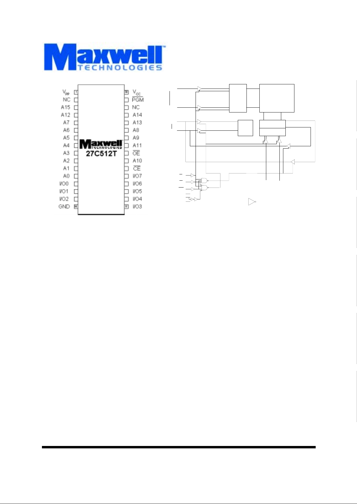
x-Decoder
1024 x 1022
Memory Matrix
Input
Data
Control
Y- Gating
Y - Decoder
H
A0-A4
A10-A11
OE
PGM
A5-A9
V
CC
V
PP
V
SS
A12-A16
I/O0
I/O15
H
CE
: High Threshhold Inverter
Logic Diagram
Page 2
Memory
2
All data sheets are subject to change without notice
©2002 Maxwell Technologies
All rights reserved.
512K (64K x 8-Bit) OTP EPROM
27C512T
02.18.02 Rev3
TABLE 1. 27C512T PINOUT DESCRIPTION
PIN SYMBOL DESCRIPTION
1VPPProgramming Voltage
2, 30 NC Not connected
12-5, 27, 26, 23,
25, 4, 28, 29, 3
A0-A15 Address Enable
22 CE
Chip Enable
24 OE
Output Enable
13-15, 17-21 I/O0 - I/O7 Data Input/Output
16 GND Ground
31 PGM
Program
32 V
CC
+5V Power Supply
TABLE 2. 27C512T ABSOLUTE MAXIMUM RATINGS
PARAMETER SYMBOL MIN MAX UNIT
Supply Voltage
1
1. Relative to VSS.
V
CC
-0.6 +7.0 V
Programming Voltage
1
V
PP
-0.6 +13.5 V
All Input and Output Voltage
1,2
2. VIN, V
OUT
, and VID min = -1.0V for pulse width < 20 ns.
V
IN
, V
OUT
-0.6 +7.0 V
A9 and OE
Voltage V
ID
-0.6 13.0 V
Operating Temperature Range T
OPR
-55 +125
°
C
Storage Temperature Range T
STG
-65 +125
°
C
TABLE 3. DELTA LIMITS
PARAMETER VARIATION
ICC1 ±10%
I
CC
2 ±10%
I
CC
3A ±10%
I
CC
3B ±10%
Page 3

Memory
3
All data sheets are subject to change without notice
©2002 Maxwell Technologies
All rights reserved.
512K (64K x 8-Bit) OTP EPROM
27C512T
02.18.02 Rev3
TABLE 4. 27C512T RECOMMENDED OPERATING CONDITIONS
PARAMETER SUBGROUPS SYMBOL MIN MAX UNITS
Supply Voltage 1 V
CC
4.5 5.5 V
Input Voltage 1 V
IL
-0.3
1
1. VIL min = -1.0V for pulse width < 50 ns.
0.8 V
1V
IH
2.2 VCC +1
2
2. V
IH
max = VCC + 1.5V for pulse width < 20 ns.
Thermal Impedance — DIP Package 1
Θ
JC
-- 1.26 °C/W
Thermal Impedance — Flat Package 1
Θ
JC
-- 1.27 °C/W
Operating Temperature Range 1 T
OPR
-55 +125
°
C
TABLE 5. 27C512T CAPACITANCE
1
1. Guaranteed by design.
PARAMETER SYMBOL MIN MAX UNIT
Input Capacitance C
IN
-- 10 pF
Output Capacitance C
OUT
-- 15 pF
TABLE 6. 27C512T DC ELECTRICAL CHARACTERISTICS FOR READ OPERATION
(VCC = 5V + 10%, VPP = VSS TO VCC, TA = -55 TO +125 °C, UNLESS OTHERWISE SPECIFIED)
PARAMETER TEST CONDITION S
UBGROUPS SYMBOL MIN TYP MAX UNIT
Input Leakage Current V
IN
= 5.5 V 1, 2, 3 I
LI
-- -- 2 µA
Output Leakage Current V
OUT
= 5.5 V/0.45 V 1, 2, 3 I
LO
-- -- 2 µA
Standby V
CC
Current CE = V
IH
1, 2, 3 I
SB
-- -- 1 mA
Operating V
CC
Current I
OUT
= 0 mA, CE = V
IL
1, 2, 3 I
CC1
-- -- 30 mA
I
OUT
= 0 mA, f = 5 MHz 1, 2, 3 I
CC2
-- -- 30
I
OUT
= 0 mA, f = 10 MHz 1, 2, 3 I
CC3
-- -- 50
V
PP
Current VPP = 5.5 V 1, 2, 3 I
PP1
-- 1 20 µA
Input Voltage 1, 2, 3 V
IH
2.2 -- -- V
1, 2, 3 V
IL
-- 0.8
Output Voltage I
OH
= -400µA 1, 2, 3 V
OH
2.4 -- -- V
I
OL
= 2.1 mA 1, 2, 3 V
OL
-- -- 0.45
Page 4

Memory
4
All data sheets are subject to change without notice
©2002 Maxwell Technologies
All rights reserved.
512K (64K x 8-Bit) OTP EPROM
27C512T
02.18.02 Rev3
TABLE 7. 27C512T AC ELECTRICAL CHARACTERISTICS FOR READ OPERATION 1,
2
(VCC = 5V + 10%, VPP = VSS TO VCC, TA = -55 TO +125 °C, UNLESS OTHERWISE SPECIFIED)
1. t
DF
is defined as the time at which the output becomes an open circuit and data is no longer driven.
2. AC electrical parameters for programming operations are not tested. These are guaranteed by design.
PARAMETER TEST CONDITION S
UBGROUPS SYMBOL MIN MAX UNIT
Address Access Time
-120
-150
-200
CE
= OE = V
IL
9, 10, 11 t
ACC
--
--
--
120
150
200
ns
Chip Enable Access Time
-120
-150
-200
OE
= V
IL
9, 10, 11 t
CE
--
--
--
120
150
200
ns
Output Enable Access Time
-120
-150
-200
CE
= V
IL
9, 10, 11 t
OE
--
--
--
60
70
70
ns
Output Hold to Address Change
-120
-150
-200
CE
= V
IL
9, 10, 11 t
OH
0
0
0
--
--
--
ns
Output Disable to High-Z
3
-120
-150
-200
3. Test conditions:
- Input pulse levels 0.45V/2.4V
- Input rise and fall times < 10 ns
- Output load 1TTL Fate + 100 pF (including scope and jig)
- Referenced levels for measuring timing 0.8V/2.0V
CE
= OE = VIL 9, 10, 11 t
DF
0
0
0
50
50
50
ns
Page 5

Memory
5
All data sheets are subject to change without notice
©2002 Maxwell Technologies
All rights reserved.
512K (64K x 8-Bit) OTP EPROM
27C512T
02.18.02 Rev3
TABLE 8. 27C512T AC ELECTRICAL CHARACTERISTICS FOR PROGRAMMING OPERATION
1,2
(VCC = 6.0V + 0.25V, VPP = 12.5V + 0.3V, TA = 25 °C)
1. t
DF
is defined as the time at which the output becomes an open circuit and data is no longer driven.
2. AC electrical parameters for programming operations are not tested. These are guaranteed by design.
PARAMETER S
UBGROUPS SYMBOL MIN TYP MAX UNIT
Address Setup Time 9 t
AS
2----µs
Address Hold Time 9 t
AH
0----µs
Data Setup Time 9 t
DS
2----µs
Data Hold Time 9 t
DH
2----µs
V
PP
Setup Time 9 t
VPS
2----µs
V
CC
Setup Time 9 t
VCS
2----µs
Output Enable Setup Time 9 t
OES
2----µs
Output Disable Time 9 t
DF
3
3. Test Conditions:
- Input pulse levels 0.45V/2.4V
- Input rise and fall times < 20 ns
- Referenced levels for measuring timing 0.8V/2.0V
0 -- 130 ns
CE
Initial Programming Pulse Width 9 t
PW
0.19 0.20 0.21 ms
CE
Overprogramming Pulse Width 9 t
OPW
0.19 -- 5.25 ms
Output Enable Hold Time 9 t
OEH
2----µs
V
PP
Recovery Time 9 t
VR
2----µs
Data Valid from Chip Enable 9 t
DV
1----µs
TABLE 9. 27C512T DC ELECTRICAL CHARACTERISTICS FOR PROGRAMMING OPERATIONS
1,2,3,4
(VCC = 6.0V + 0.25V, VPP = 12.5V + 0.3V, TA = 25 °C)
1. V
CC
must be applied before VPP and removed after VPP.
2. V
PP
must not exceed 13V, including overshoot.
3. Do not change V
PP
from VIL to 12.5V or 12.5V to VIL when CE = low.
4. DC electrical parameters for programming operations are not tested. These are guaranteed by design.
PARAMETER TEST CONDITION S
UBGROUPS SYMBOL MIN MAX UNIT
Input Leakage Current V
IN
=0V to V
CC
1ILI-- 2 µA
Operating V
CC
Current 1 I
CC
-- 30 mA
Operating V
PP
Current CE=PGM=V
IL
1IPP-- 40 mA
Input Voltage
5
5. Device reliability may be adversely affected if the device is installed or removed while V
PP
= 12.5V.
1V
IH
2.2 VCC+0.5
6
V
1V
IL
-0.1
7
0.8
Output Voltage I
OH
=-400µA 1 V
OH
2.4 -- V
I
OH
= 2.1mA 1 V
OL
-- 0.45
Page 6

Memory
6
All data sheets are subject to change without notice
©2002 Maxwell Technologies
All rights reserved.
512K (64K x 8-Bit) OTP EPROM
27C512T
02.18.02 Rev3
6. If VIH is over the specified maximum value, programming operation can not be guaranteed.
7. V
IL
min = -0.6V for pulse width < 20 ns.
TABLE 10. 27C512T MODE SELECTION
MODE
V
PP
V
CC
CE OE PGM
A
9
I/O
Read V
CC
V
CC
V
IL
V
IL
V
IH
X
1
1. X = Don’t care.
D
OUT
Output Disable V
CC
V
CC
V
IL
V
IH
V
IH
X High-Z
Standby V
CC
V
CC
V
IH
XXX High-Z
Program V
PP
V
CC
V
IL
V
IH
V
IL
XD
IN
Program Verify V
PP
V
CC
V
IL
V
IL
V
IH
XD
OUT
Page Data Latch V
PP
V
CC
V
IH
V
IL
V
IH
XD
IN
Page Program V
PP
V
CC
V
IH
V
IH
V
IL
X High-Z
Program Inhibit V
CC
V
CC
V
IL
V
IL
V
IL
X High-Z
V
PP
V
CC
V
IL
V
IH
V
IH
X High-Z
V
PP
V
CC
V
IH
V
IL
V
IL
X High-Z
V
PP
V
CC
V
IH
V
IH
V
IH
X High-Z
Identifier V
CC
V
CC
V
IL
V
IL
V
IH
V
H
2
2. 11.5V < VH < 12.5V.
ID
Page 7

Memory
7
All data sheets are subject to change without notice
©2002 Maxwell Technologies
All rights reserved.
512K (64K x 8-Bit) OTP EPROM
27C512T
02.18.02 Rev3
FIGURE 1. READ TIMING WAVEFORM
Page 8

Memory
8
All data sheets are subject to change without notice
©2002 Maxwell Technologies
All rights reserved.
512K (64K x 8-Bit) OTP EPROM
27C512T
02.18.02 Rev3
FIGURE 2. PAGE PROGRAMMING FLOWCHART
START
SET PAGE PROG. MODE
V
PP
=12.5+0.3V, VCC=6.0+ 0.25V
Address=0
n=0
Latch
Address+1
Address
Address+1
Address
Latch
Address+1
Address
Latch
Latch
Address+1
Address
B
A
A
n+1 n
SET PAGE PROG./
VERIFY MODE
V
PP
=12.5+0.3V,
V
CC
=6.0+0.25V
Program tPW=0.2ms+5%
n=25
VERIFY
Program t
OPW
=0.2ms
Last
Address?
B
SET PAGE MODE
V
CC
=5.0+0.25V, VPP=V
CC
READ
All Address
END FAIL
NOGO
GO
YES
NO
GO
NOGO
NO
YES
Page 9

Memory
9
All data sheets are subject to change without notice
©2002 Maxwell Technologies
All rights reserved.
512K (64K x 8-Bit) OTP EPROM
27C512T
02.18.02 Rev3
FIGURE 3. PAGE PROGRAMMING TIMING WAVEFORM
Page 10

Memory
10
All data sheets are subject to change without notice
©2002 Maxwell Technologies
All rights reserved.
512K (64K x 8-Bit) OTP EPROM
27C512T
02.18.02 Rev3
FIGURE 4. BYTE PROGRAMMING FLOWCHART
n+1 n
Program tPW=1ms+5%
n=25
VERIFY
Program t
OPW
=0.2ms
Last
Address?
SET PAGE MODE
V
CC
=5.0+0.25V, VPP=V
CC
READ
All Address
END FAIL
NOGO
GO
YES
NO
GO
NOGO
NO
YES
SET PROG./VERIFY MODE
V
PP
=12.5+0.3V, VCC=6.0+0.25V
START
Address=0
n=0
Address+1 Address
Page 11

Memory
11
All data sheets are subject to change without notice
©2002 Maxwell Technologies
All rights reserved.
512K (64K x 8-Bit) OTP EPROM
27C512T
02.18.02 Rev3
FIGURE 5. BYTE PROGRAMMING TIMING WAVEFORM
DEVICE IDENTIFIER MODE DESCRIPTION
The Device Identifier Mode allows binary codes to be read from th e outputs th at iden tify the manufactu rer an d the type
of device. Using this mode with programming equipment, the device will au tomatically match its own erase an d programming algorithm.
1. VCC = 5.0V + 10%.
2. A
9
= 12.0V + 0.5V.
3. A
1-A8
, A10-A16, CE, OE = VIL, PGM = VIH.
4. X = Don’t care.
27C512T SERIES IDENTIFIER CODE
IDENTIFIER A
0
I/O
7
I/O
6
I/O
5
I/O
4
I/O
3
I/O
2
I/O
1
I/O
0
HEX DATA
MANUFACTURER CODE V
IL
00000111 07
D
EVICE CODE V
IH
00111000 38
Page 12

Memory
12
All data sheets are subject to change without notice
©2002 Maxwell Technologies
All rights reserved.
512K (64K x 8-Bit) OTP EPROM
27C512T
02.18.02 Rev3
D32-04
Note: All dimensions in inches
32 PIN RAD-PAK® DUAL IN LINE PACKAGE
SYMBOL
DIMENSION
MIN NOM MAX
A -- 0.215 0.240
b 0.014 0.018 0.026
b2 0.045 0.050 0.065
c 0.008 0.010 0.018
D -- 1.600 1.680
E 0.510 0.590 0.620
eA 0.600 BSC
eA/2 0.300 BSC
e 0.100 BSC
L 0.125 0.145 0.155
Q 0.015 0.035 0.070
S1 0.005 0.025 -S2 0.005 -- --
N32
Page 13

Memory
13
All data sheets are subject to change without notice
©2002 Maxwell Technologies
All rights reserved.
512K (64K x 8-Bit) OTP EPROM
27C512T
02.18.02 Rev3
F32-09
Note: All dimensions in inches
32 PIN RAD-PAK® FLAT PACKAGE
SYMBOL
DIMENSION
MIN NOM MAX
A 0.198 0.210 0.220
b 0.015 0.017 0.020
c 0.004 0.005 0.009
D -- 0.820 0.830
E 0.472 0.480 0.488
E1 -- -- 0.498
E2 0.300 0.310 -E3 0.030 0.085 --
e 0.050 BSC
L 0.355 0.365 0.375
Q 0.055 0.065 0.075
S1 0.005 0.027 --
N32
Page 14

Memory
14
All data sheets are subject to change without notice
©2002 Maxwell Technologies
All rights reserved.
512K (64K x 8-Bit) OTP EPROM
27C512T
02.18.02 Rev3
Important Notice:
These data sheets are created using the chip manufacturers published specifications. Maxwell Technologies verifies
functionality by testing key parameters either by 100% testing, sample testing or characterization.
The specifications presented within these data sheets represent the latest and most accurate information available to
date. However, these specifications are subject to change without notice and Maxwell Technologies assumes no
responsibility for the use of this information.
Maxwell Technologies’ products are not authorized for use as critical components in life support devices or systems
without express written approval from Maxwell Technologies.
Any claim against Maxwell Technologies must be made within 90 days from the date of shipment from Maxwell Technologies. Maxwell Technologies’ liability shall be limited to replacement of defective parts.
Page 15

Memory
15
All data sheets are subject to change without notice
©2002 Maxwell Technologies
All rights reserved.
512K (64K x 8-Bit) OTP EPROM
27C512T
02.18.02 Rev3
Product Ordering Options
Model Number
Feature
Option Details
27C512T
RP
X X
-XX
Access Time
Screening Flow
Package
Radiation Feature
Base Product
Nomenclature
12 = 120 ns
15 = 150 ns
20 = 200 ns
Monolithic
S = Maxwell Class S
B = Maxwell Class B
E = Engineering (testing @ +25°C
)
I = Industrial (testing @ -55°C,
+25°C, +125°C)
D = Dual In-line Package (DIP)
F = Flat Pack
RP = R
AD-PAK® package
512K (64K x 8-Bit) OTP EPROM
 Loading...