

Page 1
Data Sheet, Rev. 1
August 2001
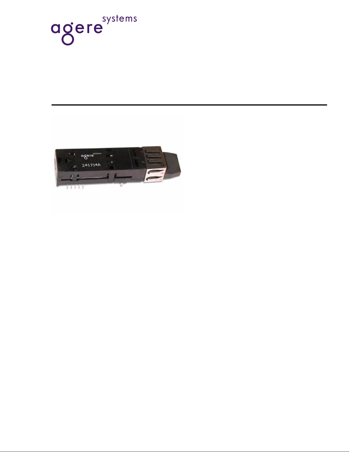
NetLight
®
2417J4A 1300 nm Laser
Gigabit Transceiver
Available in a smal l form-factor, RJ-45 size, plastic packa ge,
the 2417J4A Transceiver is a high-perf ormance, costeffective optic al transceiv er for Gigabit Ethern et 1000Base-LX
applications.
Features
■
Gigabit Ethernet 1000Base-LX compliant
■
Small form factor (SFF), RJ-45 size, multisourced
10-pin package
■
LC duplex receptacle
■
Uncooled 1300 nm laser transmitter with automatic
output power control
■
Transmitter disable input
■
TTL signal-detect output
■
Low power dissipation
■
Single 3.3 V power supply
■
Raised ECL (LVPECL) logic data interfaces
■
Operating temperature range: 0 °C to
70 °C
■
Agere Systems Inc. Reliability and Qualification
Program for built-in quality and reliability
Description
The 2417J4A transceiver is a high-speed, cost-effective optical transceiver that is compliant with the
®
IEEE
802.3z Gigabit Ethernet Physical Medium
Dependent (PMD) 1000Base-LX spe cifications usi ng
a long-wav elength laser. The transceiver featur es the
latest generation of Agere Systems optics and is
packaged in a narrow-width plastic housing with an
LC duplex receptacle. This receptacle fits into an
RJ-45 form-factor outline. The 10-pin package and
pinout conform to a multisource transceiver agreement.
The transmitter features differential LVPECL logic
level data inputs and an LVTTL logic level disable
input. The receiver f eatu res differential L VPECL logic
level data outputs and an LVTTL logic level signaldetect output.
■
Wide dynamic range receiver with InGaAs PIN
photodetector
Page 2
NetLight
2417J4A 1300 nm Laser Data Sheet, Rev. 1
Gigabit Transceiver August 2001
Absolute Maximum Rat ings
Stresses in excess of the absolute maximum ratings can cause permanent damage to the device. These are absolute stress ratings only. Functional operation of the device is not implied at these or any other conditions in excess
of those given in the operations s ections of the data sheet. Exposure to absolute maximum ratings for extended
periods can adversely affect device reliability.
Parameter Symbol Min Max Unit
Supply Voltage V
Operating Temperature Range T
Storage Case Temperature Range T
CC
stg
03.6V
C
070°C
–40 85 °C
Lead Soldering Temperature/Time — — 250/10 °C/s
Operating Wavelength Range λ 1.1 1.6 µm
Pin Information
Figure 1. 2417J4A Transceiver, 10-Pin Configuration, Top View
Table 1. Transceiver Pin Descriptions
Pin
Number
MS MS
Symbol Name/Description
Mounting Studs.
cal attachment to the circuit board. They may also provide an optional con-
nection of the transceiver to the equipment chassis ground.
1V
2V
EER
CCR
3SD
Receiver Signal Ground
Receiver Power Supply.
Signal Detect.
Normal operation: logic one output.
Fault condition: logic zero output.
4RD–
5RD+
6V
7V
8T
CCT
EET
DIS
9TD+
Received DATA
Received DATA Out.
Transmitter Power Supply.
Transmitter Signal Ground
Transmitter Disable.
Transmitter DATA In.
100 Ω resistor between the TD+ and TD– pins.
10 TD–
Transmitter DATA
12345
109876
RX
TX
Receiver
The mounting studs are provided for transceiver mechani-
.NA
Out.
Transmitter
.NA
An internal termination is provided, consisting of a
In.
See TD+ pin for terminations. LVPECL
3
0
1
-
1
Logic
Family
NA
NA
LVTTL
LVPECL
LVPECL
NA
LVTTL
LVPECL
F
)
(
1
2 Agere Systems Inc.
Page 3

Data Sheet, Rev. 1
NetLight
2417J4A 1300 nm Laser
August 2001 Gigabit Transceiver
Electrostatic Discharge
Caution: This device is susceptible to damage as
a result of electrostatic discharge (ESD).
Take proper precautions during both
handling and testing. Follow
dard
EIA
-625.
Although protection circuitry is designed into the
device, take proper precautions to avoid exposure to
ESD.
Agere Systems employs a human-body model (HBM)
for ESD susceptibility testing and protection-design
evaluation. ESD voltage thresholds are dependent on
the critical parameters used to define the model. A
standard HBM (resistance = 1.5 kΩ, capacitance = 100
pF) is widely used and, therefore, can be used for comparison purposes. The HBM ESD threshold established for the 2417J4A is ±1500 V.
EIA
®
Stan-
Application Information
The 2417 receiver section is a highly sensitive fiberoptic receiver. Although the data outputs are digital
logic lev e ls (PEC L) , the device should be thought of as
an analog component. When laying out system application boards, the 2417 transceiver should receive the
same type of consideration one would give to a sensitive analog component.
Printed-Wiring Board Layout Considerations
A fiber-optic receiver employs a very high gain, wide
bandwidth transimpedance amplifier. This amplifier
detects and amplifies signals that are only tens of nA in
amplitude when the receiver is operating near its sensitivity limit. Any unwanted signal currents that couple
into the receiver circuitry cause a decrease in the
receiver's sensitivity and can also degrade the performance of the receiver's signal detect (SD) circuit. To
minimize the coupling of unwanted noise into the
receiver, careful attention must be given to the printedwiring board layout.
Multilayer construction also permits the routing of sensitive signal traces away from high-level, high-speed
signal lines. To minimize the possibility of coupling
noise into the receiver section, high-level, high-speed
signals such as transmitter inputs and clock lines
should be routed as far away as possible from the
receiver pins.
Noise that couples into the receiver through the power
supply pins can also degrade performance. It is
recommended that the pi filter, shown in Figure 2, be
used for both the transmitter and receiver power
supplies.
Data and Signal Detect Outputs
The data and signal detect outputs of the 2417 transceiver are driven by open-emitter NPN transistors,
which have an outpu t impedance of appr o xima tely 7 Ω.
Each output can provide approximately 50 mA maximum current to a 50 Ω. load terminated to V
Due to the high switching speeds of ECL outputs,
transmission line design must be used to interconnect
components. To ensure optimum signal fidelity, both
data outputs (RD+/RD–) should be terminated identically. The signal lines connecting the data outputs to
the next device should be equal in length and have
matched impedances. Controlled impedance stripline
or microstrip construction must be used to preserve the
quality of the signal into the next component and to
minimize reflections bac k int o the receiver, which could
degrade its performance. Excessive ringing due to
reflections caused by improperly terminated signal
lines makes it difficult for the component receiving
these signals to decipher the proper logic levels and
can cause transitions to occur where none we re
intended. Also, by minimizing high-frequency ringing,
possible EMI problems can be avoided.
The signal-detect output is positiv e LVTTL logic. A logic
low at this output indicates that the optical signal into
the receiver has been interrupted or that the light level
has fallen below the minimum signal detect threshold.
This output should not be used as an error rate indicator since its switching threshold is determined only by
the magnitude of the incoming optical signal.
– 2.0 V.
CC
At a minimum, a double-sided printed-wiring board
(PWB) with a large component-side ground plane
beneath the transceiver must be used. In applications
that include many other high-speed devices, a multilayer PWB is highly recommended. This permits the
placement of power and ground on separate layers,
which allows them to be isolated from the signal lines.
Agere Systems Inc. 3
Page 4

NetLight
2417J4A 1300 nm Laser Data Sheet, Rev. 1
Gigabit Transceiver August 2001
Application Information
(continued)
Transceiver Processing
When the process plug is placed in the transceiver's optical port, the transceiver and plug can withstand normal
wave soldering and aqueous spray cleaning processes. However, the transceiver is not hermetic, and should not
be subjected to immersion in cleaning solvents. The transceiver case should not be exposed to temperatures in
excess of 125 °C. The transceiver pins can be wave soldered at 250 °C for up to 10 seconds. The process plug
should only be used once. After rem ovi ng the process plug fr om the tr ansceiv er, it must not be used again as a process plug; however, if it has not been contaminated, it can be reused as a dust cover.
Transceiver Optical and Electrical Characteristics
Table 2. Transmitter Optical and Electrical Characteristics
Parameter Symbol Min Max Unit
Average Optical Output Power (EOL):
Single-mode Fiber (10 µm)
Optical Wavelength λ
Spectral Width ∆λ
Dynamic Extinction Ratio EXT 9 — dB
Rise/Fall Time,20%—80% t
Output Optical Eye Compliant with
Power Supply Current I
Input Data Voltage:
Low
High
Transmit Disable Voltage V
Transmit Enable Voltage V
(T
= 0 °C to 70 °C; VCC = 3.135 V—3.465 V)
A
O
P
–11.0 –3.0 dBm
C
RMS
R,tF
1270 1355 nm
—4nm
— 260 ps
IEEE
802.3Z
Eye Mask requirements
CCT
V
V
EN
IL
IH
D
—150mA
VCC – 2.0
CC
V
– 1.2
VCC – 1.3 V
EE
V
CC
– 1.6
V
CC
V
– 0.8
CC
VEE + 0.8 V
V
V
V
Table 3. Receiver Optical and Electrical Characteristics
(T
= 0 °C to 70 °C; VCC = 3.135 V—3.465 V)
A
Parameter Symbol Min Max Unit
Average Sensitivity* P
Maximum Input Power* P
I
MAX
–19 — dBm
—–3dBm
Return Loss — 12 — dB
Link Status Switching Threshold:
Decreasing Light
Increasing Light
LST
LST
D
I
—
—
–20.5
–20.0
dBm
dBm
Link Status Hysteresis HYS 0.5 — dB
Power Supply Current I
CCR
— 100 mA
Output Data Voltage/Clock Voltage:
Low
High
OL
V
OH
V
VCC – 1.81
CC
V
– 1.025
V
V
CC
– 1.62
CC
– 0.88
V
V
Signal-detect Voltage:
Low
High
* For 1 x 10
–10
BER with an optical input using 223 – 1 PRBS.
OL
V
OH
V
0.0
2.4
0.8
V
CC
V
V
4 Agere Systems Inc.
Page 5

Data Sheet, Rev. 1
NetLight
2417J4A 1300 nm Laser
August 2001 Gigabit Transceiver
Qualification and Reliability
To help ensure high product reliabilit y an d customer sati sfaction, Agere Systems is committed to an intensive quality program that starts in the design phase and proceeds through the manufacturing process. Optoelectronic modules are qualified to Agere Systems internal standards using MIL-STD-883 test methods and procedures and
using sampling techniques consistent with
Telcordia Technologies
to pass an extensive and rigorous set of qualification tests.
®
requirements. The 24 17 transceiver is required
In addition, the design, development, and manufacturing facilities ofthe Agere Systems Optoelectronics unit have
®
been certified to be in full compliance with the latest
ISO
9001 quality system standards.
Electrical Schematic
EET
TRANSMITTER
DRIVER
SFF TRANSCEIVER
RECEIVER
POST-
PREAMP
AMPLIFIER
V
TD–
100 Ω R
TD+
V
V
RD+
RD–
SD
CCT
CCR
10
7
9
6
2
5
4
3
L2
C4 C5
C2 C3 C1
L1
CC
V
L1 = L2 = 1 µH—4.7 µH*
C1 = C2 = 10 nF
C3 = 4.7 µF—10 µF
C4 = C5 = 4.7 µF—10 µF
†
EER
V
* Ferrite beads can be used as an opt ion.
† For all capacitors, MLC caps are recommended.
1
1-968 (F).a
Figure 2. Power Supply Filtering for the Small Form Factor Transceiver
Agere Systems Inc. 5
Page 6

NetLight
2417J4A 1300 nm Laser Data Sheet, Rev. 1
Gigabit Transceiver August 2001
Application Schematics
VCC (+3.3 V)
TD+
Ω
100
(A) TRANSMITTER INTERFACE (LVPECL TO LVPECL)
VCC (+3.3 V)
RD+
RD–
130
TD–
Ω
Z = 50 Ω
Z = 50 Ω
Z = 50 Ω
Z = 50 Ω
Ω
130
130
Ω
100
CC
V
LVPECL
130
CC
V
Ω
(+3.3 V)
Ω
(+3.3 V)
LVPECL
(B) RECEIVER INTERFACE (LVPECL TO LVPECL)
Figure 3. 3.3 V Transceiver Interface with 3.3 V ICs
1-1033 (F)
6 Agere Systems Inc.
Page 7

Data Sheet, Rev. 1
NetLight
2417J4A 1300 nm Laser
August 2001 Gigabit Transceiver
Outline Diagrams
Dimensions are in inches and (millimeters).
Package Outline
1.914
(48.62)
0.535 MAX
(13.59)
0.246
(6.25)
0.386 MAX
(9.80)
0.014
(0.36)
0.018
(0.46)
0.280
(7.11)
0.125 (3.17)
0.070 (1.78)
0.700 0.734
(17.78) (18.64)
0.400
(10.16)
0.150
(3.81)
1-1032 (F).b
Agere Systems Inc. 7
Page 8

NetLight
2417J4A 1300 nm Laser Data Sheet, Rev. 1
Gigabit Transceiver August 2001
Outline Diagrams
Printed-Wiring Board Layout
(continued)
, †
*
Dimensions are in inches and (millimeters).
3.00
(0.118)
A
∅
(2x)
2.29 MAX
AREA FOR EYELETS
(0.090)
6.00
(0.236)
3.00
(0.118)
3.08
(0.121)
7.59
(0.299)
13.34
(0.525)
(2x)
(0.055 ± 0.004)
4.57
(0.180)
7.11
(0.280)
(9x) 1.78
(0.070)
∅
(2x)
0.81 ± 0.1
(0.032 ± 0.004)
0.00 M A
∅
∅
1.4 ± 0.1 NOTE 1
0.00 M A
∅
8.89
(0.350)
16.00 REF
(0.630)
2.00 (0.79)
(2x)
∅
2.29 MAX
(0.090)
2.01
(0.79)
9.59
(0.378)
10.16
(0.400)
NOTES:
1. HOLES FOR MOUNTING STUDS MUST BE TIED TO CHASSIS GROUND.
2. HOLES FOR HOUSING LEADS MUST BE TIED TO SIGNAL GROUND.
3.56
(0.140)
∅
(4x)
1.4 ± 0.1 NOTE 2
(0.055 ± 0.004)
0.00 M A
∅
1-1271(F)
* The hatched areas are k eep-out areas reserved for ho using standoffs. No metal t races of ground connection in keep-out area.
† Twenty-pin module shown; 10-pin module requires only 16 PWB holes.
8 Agere Systems Inc.
Page 9

Data Sheet, Rev. 1
NetLight
2417J4A 1300 nm Laser
August 2001 Gigabit Transceiver
Outline Diagrams
(continued)
Recommended Panel Opening
Dimensions are in inches and (millimeters).
0.560
(14.22)
Laser Safety Information
0.400
(10.16)
0.590 TO 0.620
(14.99 TO 15.75)
0.039 TO 0.098
(1.00 TO 2.49)
1-1088(F).d
Class I Laser Product
FDA/CDRH Class 1 laser product. All versions of the transceiver are Class I laser products per CDRH, 21 CFR
1040 Laser Safety requirements. All versions are Class I laser products per
has been certified with the FDA under accession number 9520668.
CAUTION: Use of controls, adjustments, and procedures other than those specified herein may result in
hazardous laser radiation exposure.
This product complies with 21 CFR 1040.10 and 1040.11.
Wavelength = 1.3 µm
Maximum power = 1.0 mW
Because of size constraints, laser safety labeling is not affixed to the module but is attached to the outside of the
shipping carton.
Product is not shipped with power supply.
NOTICE
Unterminated optical receptacles may emit laser radiation.
Do not view with optical instruments.
®
IEC
60825-1:1993. The transceiver
Agere Systems Inc. 9
Page 10

NetLight
2417J4A 1300 nm Laser Data Sheet, Rev. 1t
Gigabit Transceiver August 2001
Ordering Information
Description Device Code Comcode
2 x 5 Single-mode SFF LC Receptacle Transceiver for
1000Base-LX Applications
2417J4A 108282229
IEEE
is a registered trademark of The Instit ute of Electrical and Electronics Engineers, Inc.
EIA
is a registered trademark of The Electronic Industries Association.
Telcordia Technologies
ISO
is a registred trademark of The International Organization for Standardization.
IEC
is a registered trademark of The International Electrotechnical Commission.
For additional information, contact your Agere S y s tems A cc ount Manager or the following:
INTERNET:
E-MAIL:
N. AMERICA:Agere Systems Inc., 555 Union Boulevard, Room 30L-15P-BA, Allentown, PA 18109-3286
ASIA: Agere Systems Hong Kong Ltd., Suites 3201 & 3210-12, 32/F, Tower 2, The Gateway, Harbour City, Kowloon
EUROPE:
Agere Systems Inc. reserves the right to make changes to the product(s) or information contained herein without notice. No liability is assumed as a result of their use or application.
is a registered trademark of Agere Systems Inc.
Copyright © 2001 Agere Systems Inc.
All Rights Reserved
August 2001
DS00-105OPTO-1 (Replaces DS00-105OPTO)
is a registered trademark of Bell Communications Research, Inc.
http://www.agere.com
docmaster@agere.com
1-800-372-2447
Tel. (852) 3129-2000
CHINA:
JAPAN:
Tel. (44) 7000 624624
, FAX 610-712-4106 (In CANADA:
(86) 21-5047-1212
(81) 3-5421-1600
, FAX (852) 3129-2020
(Shanghai),
(Tokyo), KOREA:
, FAX (44) 1344 488 045
(86) 10-6522-5566
1-800-553-2448
(82) 2-767-1850
(Beijing),
(Seoul), SINGAPORE:
, FAX 610-712-4106)
(86) 755-695-7224
(65) 778-8833
(Shenzhen)
, TAIWAN:
(886) 2-2725-5858
(Taipei)
NetLight
 Loading...