

Page 1

A28F010
1024K (128K x 8) CMOS FLASH MEMORY
(Automotive)
Y
Automotive Temperature Range:
b
40§Ctoa125§C
Y
Flash Memory Electrical Chip-Erase
Ð 1 Second Typical Chip-Erase
Y
Quick-Pulse Programming Algorithm
Ð10 ms Typical Byte-Program
Ð 2 Second Chip-Program
Y
1,000 Erase/Program Cycles Minimum
over Automotive Temperature Range
Y
12.0Vg5% V
Y
High-Performance Read
PP
Ð 120 ns Maximum Access Time
Y
CMOS Low Power Consumption
Ð 30 mA Maximum Active Current
Ð 300 mA Maximum Standby Current
Y
Integrated Program/Erase Stop Timer
Y
Command Register Architecture for
Microprocessor/Microcontroller
Compatible Write Interface
Y
Noise Immunity Features
g
Ð
10% VCCTolerance
Ð Maximum Latch-Up Immunity
through EPI Processing
Y
ETOXTMIII Flash Nonvolatile Memory
Technology
Ð EPROM-Compatible Process Base
Ð High-Volume Manufacturing
Experience
Y
JEDEC-Standard Pinouts
Ð 32-Pin Plastic DIP
Ð 32-Lead PLCC
(See Packaging Spec., OrderÝ231369)
Intel’s 28F010 CMOS flash memory offers the most cost-effective and reliable alternative for read/write
random access nonvolatile memory. The 28F010 adds electrical chip-erasure and reprogramming to familiar
EPROM technology. Memory contents can be rewritten: in a test socket; in a PROM-programmer socket; onboard during subassembly test; in-system during final test; and in-system after-sale. The 28F010 increases
memory flexibility, while contributing to time- and cost-savings.
The 28F010 is a 1024-kilobit nonvolatile memory organized as 131,072 bytes of 8 bits. Intel’s 28F010 is
offered in 32-pin Plastic DIP or 32-lead PLCC packages. Pin assignments conform to JEDEC standards.
Extended erase and program cycling capability is designed into Intel’s ETOX
TM
III (EPROM Tunnel Oxide)
process technology. Advanced oxide processing, an optimized tunneling structure, and lower electric field
combine to extend reliable cycling beyond that of traditional EEPROMs. With the 12.0V V
28F010 performs a minimum of 1,000 erase and program cycles well within the time limits of the Quick-Pulse
supply, the
PP
Programming and Quick-Erase algorithms.
Intel’s 28F010 employs advanced CMOS circuitry for systems requiring high-performance access speeds, low
power consumption, and immunity to noise. Its 120 nanosecond access time provides no-WAIT-state performance for a wide range of microprocessors and microcontrollers. Maximum standby current of 300 mA translates into power savings when the device is deselected. Finally, the highest degree of latch-up protection is
achieved through Intel’s unique EPI processing. Prevention of latch-up is provided for stresses up to 100 mA
on address and data pins, from
b
1V to V
CC
a
1V.
With Intel’s ETOX III process base, the 28F010 leverages years of EPROM experience to yield the highest
levels of quality, reliability, and cost-effectiveness.
In order to meet the rigorous environmental requirements of automotive applications, Intel offers the 28F010 in
extended automotive temperature range. Read and write characteristics are guaranteed over the range of
b
40§Ctoa125§C ambient.
*Other brands and names are the property of their respective owners.
Information in this document is provided in connection with Intel products. Intel assumes no liability whatsoever, including infringement of any patent or
copyright, for sale and use of Intel products except as provided in Intel’s Terms and Conditions of Sale for such products. Intel retains the right to make
changes to these specifications at any time, without notice. Microcomputer Products may have minor variations to this specification known as errata.
November 1995COPYRIGHT©INTEL CORPORATION, 1995 Order Number: 290266-004
Page 2
A28F010
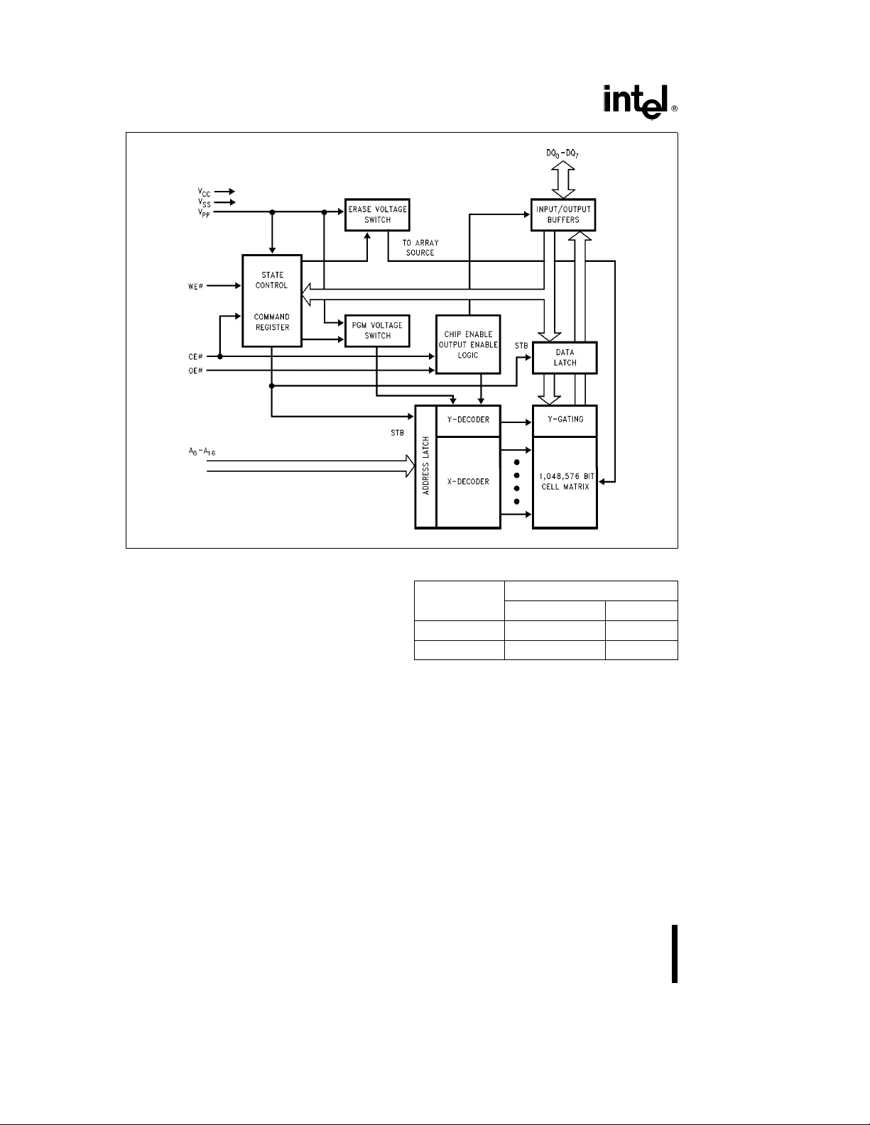
Figure 1. 28F010 Block Diagram
AUTOMOTIVE TEMPERATURE FLASH
MEMORIES
The Intel Automotive Flash memories have received
additional processing to enhance product characteristics. The automotive temperature range is
a
to
125§C during the read/write/erase/program
operations.
2
b
40§C
Speed
Versions
150 AP AN
120 AP AN
Packaging Options
Plastic DIP PLCC
290266– 1
Page 3
A28F010
28F010
290266– 3
290266– 2
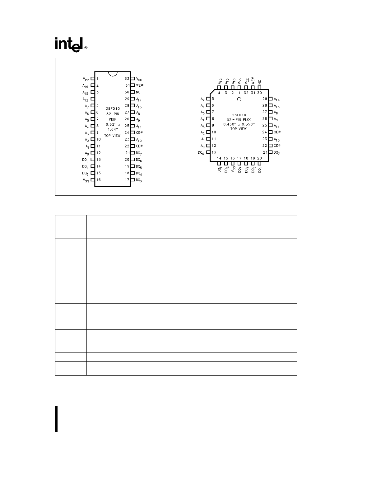
Figure 2. 28F010 Pin Configurations
Table 1. Pin Description
Symbol Type Name and Function
A0–A
16
DQ0–DQ7INPUT/OUTPUT DATA INPUT/OUTPUT: Inputs data during memory write cycles;
Ý
CE
Ý
OE
Ý
WE
V
PP
V
CC
V
SS
NC NO INTERNAL CONNECTION to device. Pin may be driven or left
INPUT ADDRESS INPUTS for memory addresses. Addresses are internally
latched during a write cycle.
outputs data during memory read cycles. The data pins are active high
and float to tri-state OFF when the chip is deselected or the outputs
are disabled. Data is internally latched during a write cycle.
INPUT CHIP ENABLE: Activates the device’s control logic, input buffers,
Ý
decoders and sense amplifiers. CE
is active low; CEÝhigh
deselects the memory device and reduces power consumption to
standby levels.
INPUT OUTPUT ENABLE: Gates the devices output through the data buffers
Ý
during a read cycle. OE
is active low.
INPUT WRITE ENABLE: Controls writes to the control register and the array.
Write enable is active low. Addresses are latched on the falling edge
and data is latched on the rising edge of the WE
s
Note: With V
6.5V, memory contents cannot be altered.
PP
Ý
pulse.
ERASE/PROGRAM POWER SUPPLY for writing the command
register, erasing the entire array, or programming bytes in the array.
DEVICE POWER SUPPLY (5Vg10%)
GROUND
floating.
3
Page 4

A28F010
APPLICATIONS
The 28F010 flash-memory adds electrical chip-erasure and reprogrammability to EPROM non-volatility
and ease of use. The 28F010 is ideal for storing
code or data-tables in applications where periodic
updates are required. The 28F010 also serves as a
dense, nonvolatile data acquisition and storage medium.
The need for code updates pervades all phases of a
system’s lifeÐfrom prototyping to system manufacture to after-sale service. In the factory, during prototyping, revisions to control code necessitate ultraviolet erasure and reprogramming of EPROM-based
prototype codes. The 28F010 replaces the 15- to
20-minute ultraviolet erasure with one-second electrical erasure. Electrical chip-erasure and reprogramming occur in the same workstation or PROMprogrammer socket.
Diagnostics, performed at subassembly or final assembly stages, often require the socketing of
EPROMs. Socketed test codes are ultimately replaced with EPROMs containing the final program.
With electrical chip-erasure and reprogramming, the
28F010 is soldered to the circuit board. Test codes
are programmed into the 28F010 as it resides on the
circuit board. Ultimately, the final code can be downloaded to the device. The 28F010’s in-circuit alterability eliminates unnecessary handling and less-reliable socketed connections, while adding greater
test flexibility.
Material and labor costs associated with code
changes increase at higher levels of system integrationÐthe most costly being code updates after sale.
Code ‘‘bugs’’, or the desire to augment system functionality, prompt after-sale code updates. Field revisions to EPROM-based code require the removal of
EPROM components or entire boards.
Designing with the in-circuit alterable 28F010 eliminates socketed memories, reduces overall material
costs, and drastically cuts the labor costs associated with code updates. With the 28F010, code updates are implemented locally via an edge-connector, or remotely over a serial communication link.
The 28F010’s electrical chip-erasure, byte reprogrammability, and complete nonvolatility fit well with
data accumulation needs. Electrical chip-erasure
gives the designer a ‘‘blank-slate’’ in which to log
data. Data can be periodically off-loaded for analysisÐerasing the slate and repeating the cycle. Or,
multiple devices can maintain a ‘‘rolling window’’ of
accumulated data.
With high density, nonvolatility, and extended cycling
capability, the 28F010 offers an innovative alternative for mass storage. Integrating main memory and
backup storage functions into directly executable
flash memory boosts system performance, shrinks
system size, and cuts power consumption. Reliability
exceeds that of electromechanical media, with
greater durability in extreme environmental conditions.
A high degree of on-chip feature integration simplifies memory-to-processor interfacing. Figure 3 depicts two 28F010s tied to the 80C186 system bus.
The 28F010’s architecture minimizes interface circuitry needed for complete in-circuit updates of
memory contents.
With cost-effective in-system reprogramming and
extended cycling capability, the 28F010 fills the
functionality gap between traditional EPROMs and
EEPROMs. EPROM-compatible specifications,
straightforward interfacing, and in-circuit alterability
allows designers to easily augment memory flexibility and satisfy the need for updatable nonvolatile
storage in today’s designs.
4
Page 5
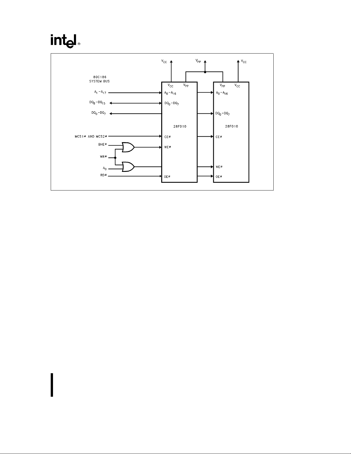
Figure 3. 28F010 in a 80C186 System
A28F010
290266– 4
PRINCIPLES OF OPERATION
Flash-memory augments EPROM functionality with
in-circuit electrical erasure and reprogramming. The
28F010 introduces a command register to manage
this new functionality. The command register allows
for: 100% TTL-level control inputs; fixed power supplies during erasure and programming; and maximum EPROM compatibility.
In the absence of high voltage on the V
28F010 is a read-only memory. Manipulation of the
external memory-control pins yields the standard
EPROM read, standby, output disable, and Intelligent Identifier operations.
The same EPROM read, standby, and output disable
operations are available when high voltage is applied to the V
enables erasure and programming of the device. All
functions associated with altering memory contentsÐIntelligent Identifier, erase, erase verify, program, and program verifyÐare accessed via the
command register.
Commands are written to the register using standard
microprocessor write timings. Register contents
serve as input to an internal state-machine which
controls the erase and programming circuitry. Write
cycles also internally latch addresses and data
pin. In addition, high voltage on V
PP
PP
pin, the
PP
needed for programming or erase operations. With
the appropriate command written to the register,
standard microprocessor read timings output array
data, access the Intelligent Identifier codes, or output data for erase and program verification.
Integrated Program/Erase Stop Timer
Successive command write cycles define the durations of program and erase operations; specifically,
the program or erase time durations are normally
terminated by associated program or erase verify
commands. An integrated stop timer provides simplified timing control over these operations; thus eliminating the need for maximum program/erase timing
specifications. Program and erase pulse durations
are minimums only. When the stop timer terminates
a program or erase operation, the device enters an
inactive state and remains inactive until receiving the
appropriate verify or reset command.
Write Protection
The command register is only alterable when VPPis
at high voltage. Depending upon the application, the
system designer may choose to make the V
er supply switchableÐavailable only when memory
updates are desired. When high voltage is removed,
PP
pow-
5
Page 6
A28F010
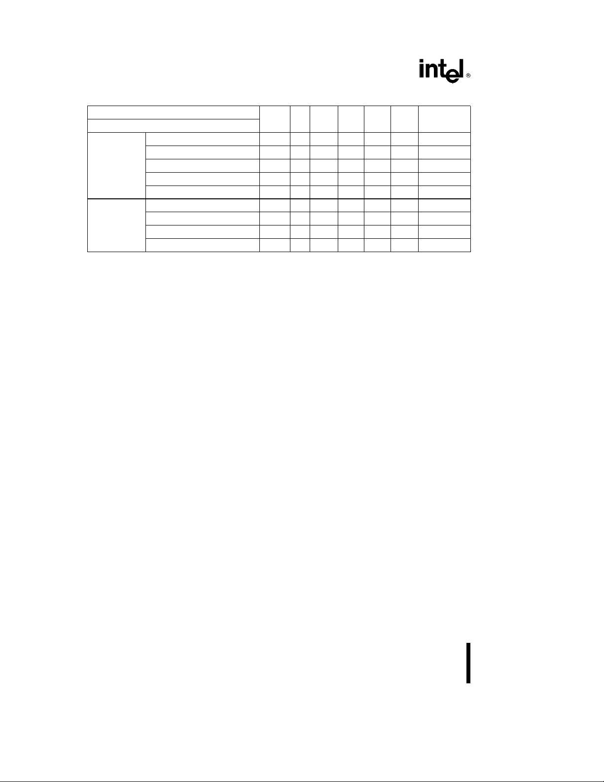
Table 2. 28F010 Bus Operations
Pins
Operation
Read V
Output Disable V
READ-ONLY
Standby V
Intelligent Identifier (Mfr)
Intelligent Identifier (Device)
(2)
(2)
Read V
READ/WRITE
Output Disable V
(5)
Standby
Write V
NOTES:
may be ground, a no-connect with a resistor tied to ground, ors6.5V. V
1. V
PPL
for the device. Refer to D.C. Characteristics. When V
2. Manufacturer and device codes may also be accessed via a command register write sequence. Refer to Table 3. All other
addresses low.
is the Intelligent Identifier high voltage. Refer to DC Characteristics.
3. V
ID
4. Read operations with V
5. With V
6. Refer to Table 3 for valid Data-In during a write operation.
7. X can be V
at high voltage, the standby current equals I
PP
or VIH.
IL
e
V
PP
may access array data or the Intelligent Identifier codes.
PPH
the contents of the register default to the read command, making the 28F010 a read-only memory.
Memory contents cannot be altered.
Or, the system designer may choose to ‘‘hardwire’’
V
, making the high voltage supply constantly
PP
available. In this instance, all operations are performed in conjunction with the command register.
The 28F010 is designed to accommodate either design practice, and to encourage optimization of the
processor-memory interface.
The two-step Program/Erase write sequence to the
Command Register provides additional software
write protection.
BUS OPERATIONS
Read
The 28F010 has two control functions, both of which
must be logically active, to obtain data at the outputs. Chip-Enable (CE
Ý
) is the power control and
should be used for device selection. Output-Enable
Ý
(OE
) is the output control and should be used to
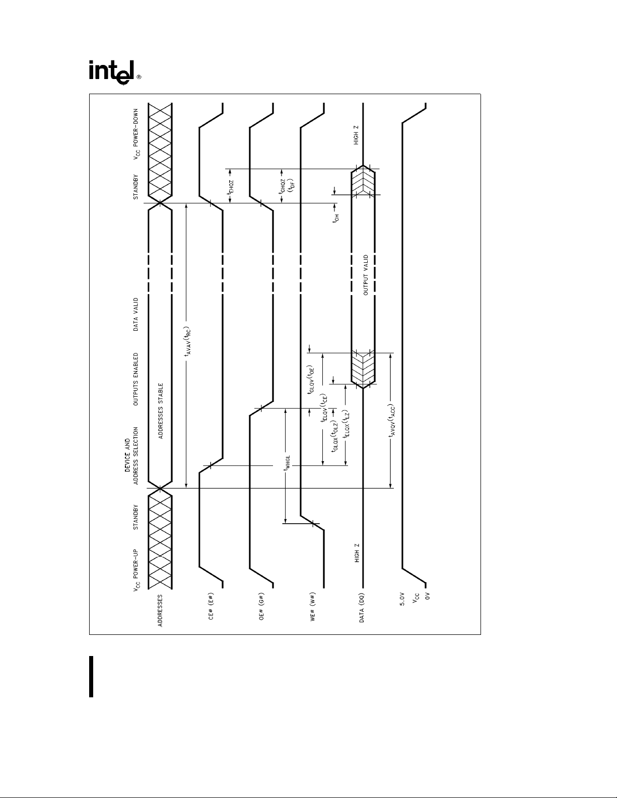
gate data from the output pins, independent of device selection. Figure 6 illustrates read timing waveforms.
When V
active. This permits reading the data in the array and
is low (V
PP
), the read only operation is
PPL
outputting the Intelligent Identifier codes (see Ta-
(1)
V
PP
PPLA0
PPL
PPL
V
PPLVILVID
V
PPLVIHVID
PPHA0
PPH
V
PPH
PPHA0
e
V
PP
PPL
a
CC
A0A9CEÝOEÝWEÝDQ0–DQ
A
V
V
9
IL
XXVILV
VIHData Out
IL
VIHTri-State
IH
XXVIHX X Tri-State
(3)
V
V
IL
(3)
V
IL
A
V
9
IL
XXVILV
VIHDatae89H
IL
V
VIHDataeB4H
IL
V
VIHData Out
IL
VIHTri-State
IH
XXVIHX X Tri-State
A
V
V
9
IL
is the programming voltage specified
memory contents can be read but not written or erased.
IPP(standby).
ble 2). When V
tion of the device is the read only mode. This allows
PPH
is high (V
PP
VILData In
IH
), the default condi-
PPH
(6)
reading the data in the array. Further functionality is
achieved though the Command Register as shown
in Table 3.
Output Disable
With Output-Enable at a logic-high level (V
from the device is disabled. Output pins are placed
), output
IH
in a high-impedance state.
Standby
With Chip-Enable at a logic-high level, the standby
operation disables most of the 28F010’s circuitry
and substantially reduces device power consumption. The outputs are placed in a high-impedance
state, independent of the Output-Enable signal. If
the 28F010 is deselected during erasure, programming, or program/erase verification, the device
draws active current until the operation is terminated.
Intelligent Identifier Operation
The Intelligent Identifier operation outputs the manufacturer code (89H) and device code (B4H). Programming equipment automatically matches the
device with its proper erase and programming
algorithms.
7
(4)
6
Page 7
A28F010
With Chip-Enable and Output-Enable at a logic low
level, raising A9 to high voltage V
teristics) activates the operation. Data read from lo-
(see DC Charac-
ID
cations 0000H and 0001H represent the manufacturer’s code and the device code, respectively.
used to store the command, along with address and
data information needed to execute the command.
The command register is written by bringing WriteEnable to a logic-low level (V
low. Addresses are latched on the falling edge of
The manufacturer- and device-codes can also be
read via the command register, for instances where
the 28F010 is erased and reprogrammed in the tar-
Write-Enable, while data is latched on the rising
edge of the Write-Enable pulse. Standard microproc-
essor write timings are used.
get system. Following a write of 90H to the command register, a read from address location 0000H
outputs the manufacturer code (89H). A read from
address 0001H outputs the device code (B4H).
Write
Device erasure and programming are accomplished
via the command register, when high voltage is applied to the V
serve as input to the internal state-machine. The
pin. The contents of the register
PP
state-machine outputs dictate the function of the
device.
Refer to A.C. Write Characteristics and the Erase/
Programming Waveforms for specific timing
parameters.
COMMAND DEFINITIONS
When low voltage is applied to the V
tents of the command register default to 00H, en-
abling read-only operations.
Placing high voltage on the V
write operations. Device operations are selected by
writing specific data patterns into the command regThe command register itself does not occupy an addressable memory location. The register is a latch
ister. Table 3 defines these 28F010 register
commands.
Table 3. Command Definitions
Command Cycles
Bus
Req’d Operation
First Bus Cycle Second Bus Cycle
(1)
Address
(2)
Data
Read Memory 1 Write X 00H
Read Intelligent Identifier Codes
Set-up Erase/Erase
Erase Verify
(5)
(5)
Set-up Program/Program
Program Verify
(7)
Reset
(6)
(4)
2 Write X 90H Read IA ID
2 Write X 20H Write X 20H
2 Write EA A0H Read X EVD
(6)
2 Write X 40H Write PA PD
2 Write X C0H Read X PVD
2 Write X FFH Write X FFH
(3)
Operation
), while Chip-Enable is
IL
pin, the con-
PP
pin enables read/
PP
(1)
Address
(2)
Data
(3)
NOTES:
1. Bus operations are defined in Table 2.
e
Identifier address: 00H for manufacturer code, 01H for device code.
2. IA
e
Address of memory location to be read during erase verify.
EA
e
Address of memory location to be programmed.
PA
Addresses are latched on the falling edge of the Write-Enable pulse.
e
Data read from location IA during device identification (Mfre89H, DeviceeB4H).
3. ID
e
Data read from location EA during erase verify.
EVD
e
Data to be programmed at location PA. Data is latched on the rising edge of Write-Enable.
PD
e
Data read from location PA during program verify. PA is latched on the Program command.
PVD
4. Following the Read Intelligent ID command, two read operations access manufacturer and device codes.
5. Figure 5 illustrates the Quick-Erase Algorithm.
6. Figure 4 illustrates the Quick-Pulse Programming Algorithm.
7. The second bus cycle must be followed by the desired command register write.
7
Page 8

A28F010
Read Command
While VPPis high, for erasure and programming,
memory contents can be accessed via the read
command. The read operation is initiated by writing
00H into the command register. Microprocessor
read cycles retrieve array data. The device remains
enabled for reads until the command register contents are altered.
The default contents of the register upon V
er-up is 00H. This default value ensures that no spu-
PP
pow-
rious alteration of memory contents occurs during
the V
hard-wired to the 28F010, the device powers-up and
power transition. Where the VPPsupply is
PP
remains enabled for reads until the command-register contents are changed. Refer to the A.C. Read
Characteristics and Waveforms for specific timing
parameters.
Intelligent Identifier Command
Flash-memories are intended for use in applications
where the local CPU alters memory contents. As
such, manufacturer- and device-codes must be accessible while the device resides in the target system. PROM programmers typically access signature
codes by raising A9 to a high voltage. However, multiplexing high voltage onto address lines is not a desired system-design practice.
The 28F010 contains an inteligent Identifier operation to supplement traditional PROM-programming
methodology. The operation is initiated by writing
90H into the command register. Following the command write, a read cycle from address 0000H retrieves the manufacturer code of 89H. A read cycle
from address 0001H returns the device code of
B4H. To terminate the operation, it is necessary to
write another valid command into the register.
high voltage is applied to the V
of this high voltage, memory contents are protected
pin. In the absence
PP
against erasure. Refer to A.C. Erase Characteristics
and Waveforms for specific timing parameters.
Erase-Verify Command
The erase command erases all bytes of the array in
parallel. After each erase operation, all bytes must
be verified. The erase verify operation is initiated by
writing A0H into the command register. The address
for the byte to be verified must be supplied as it is
latched on the falling edge of the Write-Enable
pulse. The register write terminates the erase opera-
tion with the rising edge of its Write-Enable pulse.
The 28F010 applies an internally-generated margin
voltage to the addressed byte. Reading FFH from
the addressed byte indicates that all bits in the byte
are erased.
The erase-verify command must be written to the
command register prior to each byte verification to
latch its address. The process continues for each
byte in the array until a byte does not return FFH
data, or the last address is accessed.
In the case where the data read is not FFH, another
erase operation is performed. (Refer to Set-up
Erase/Erase). Verification then resumes from the
address of the last-verified byte. Once all bytes in
the array have been verified, the erase step is com-
plete. The device can be programmed. At this point,
the verify operation is terminated by writing a valid
command (e.g. Program Set-up) to the command
register. Figure 5, the Quick-Erase algorithm, illus-
trates how commands and bus operations are com-
bined to perform electrical erasure of the 28F010.
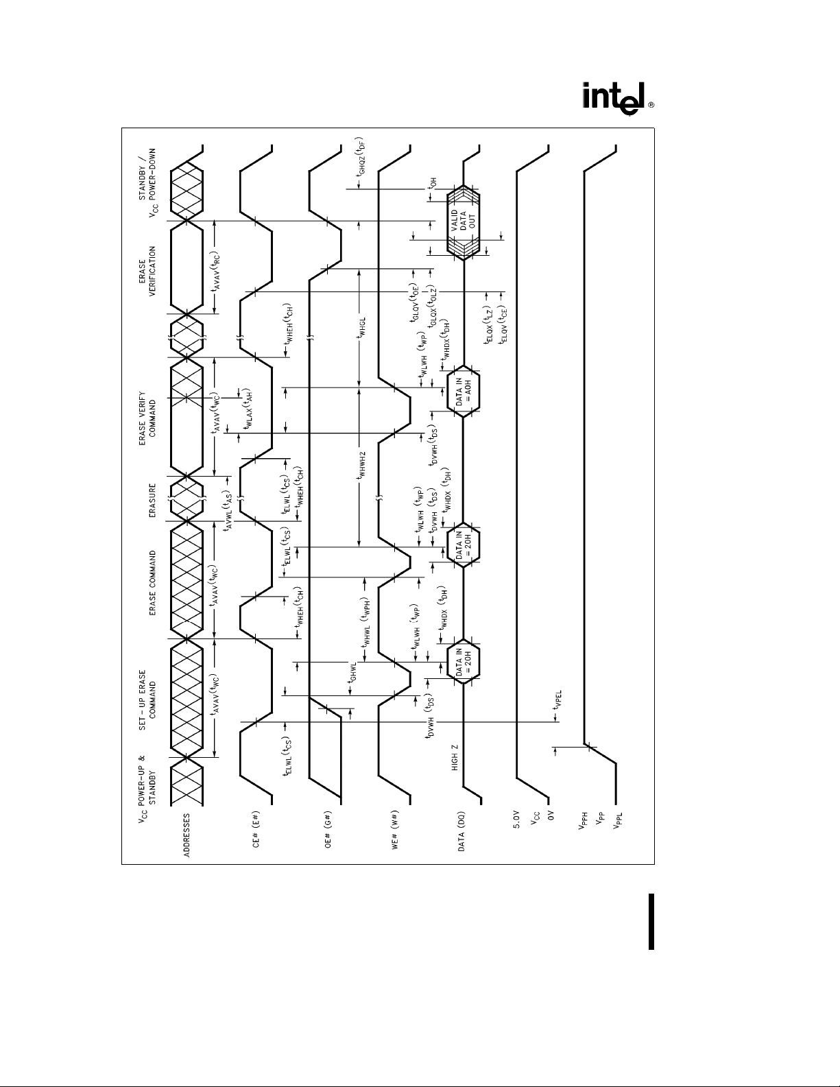
Refer to A.C. Erase Characteristics and Waveforms
for specific timing parameters.
Set-up Erase/Erase Commands
Set-up Erase is a command-only operation that
stages the device for electrical erasure of all bytes in
the array. The set-up erase operation is performed
by writing 20H to the command register.
To commence chip-erasure, the erase command
(20H) must again be written to the register. The
erase operation begins with the rising edge of the
Write-Enable pulse and terminates with the rising
edge of the next Write-Enable pulse (i.e., Erase-Verify Command).
This two-step sequence of set-up followed by execution ensures that memory contents are not accidentally erased. Also, chip-erasure can only occur when
8
Set-up Program/Program Commands
Set-up program is a command-only operation that
stages the device for byte programming. Writing 40H
into the command register performs the set-up
operation.
Once the program set-up operation is performed,
the next Write-Enable pulse causes a transition to
an active programming operation. Addresses are in-
ternally latched on the falling edge of the Write-En-
able pulse. Data is internally latched on the rising
edge of the Write-Enable pulse. The rising edge of
Write-Enable also begins the programming opera-
tion. The programming operation terminates with the
next rising edge of Write-Enable, used to write the
program-verify command. Refer to A.C. Program-
Page 9

A28F010
ming Characteristics and Waveforms for specific
timing parameters.
Program-Verify Command
The 28F010 is programmed on a byte-by-byte basis.
Byte programming may occur sequentially or at random. Following each programming operation, the
byte just programmed must be verified.
The program-verify operation is initiated by writing
C0H into the command register. The register write
terminates the programming operation with the rising edge of its Write-Enable pulse. The program-verify operation stages the device for verification of the
byte last programmed. No new address information
is latched.
The 28F010 applies an internally-generated margin
voltage to the byte. A microprocessor read cycle
outputs the data. A successful comparison between
the programmed byte and true data means that the
byte is successfully programmed. Programming then
proceeds to the next desired byte location. Figure 4,
the 28F010 Quick-Pulse Programming algorithm, illustrates how commands are combined with bus operations to perform byte programming. Refer to A.C.
Programming Characteristics and Waveforms for
specific timing parameters.
Reset Command
A reset command is provided as a means to safely
abort the erase- or program-command sequences.
Following either set-up command (erase or program)
with two consecutive writes of FFH will safely abort
the operation. Memory contents will not be altered.
A valid command must then be written to place the
device in the desired state.
ty of oxide defects in the region. Finally, the peak
electric field during erasure is approximately 2 MV/
cm lower than EEPROM. The lower electric field
greatly reduces oxide stress and the probability of
failureÐincreasing time to wearout by a factor of
100,000,000.
The device is programmed and erased using Intel’s
Quick-Pulse Programming and Quick-Erase algo-
rithms. Intel’s algorithmic approach uses a series of
operations (pulses), along with byte verification, to
completely and reliably erase and program the de-
vice.
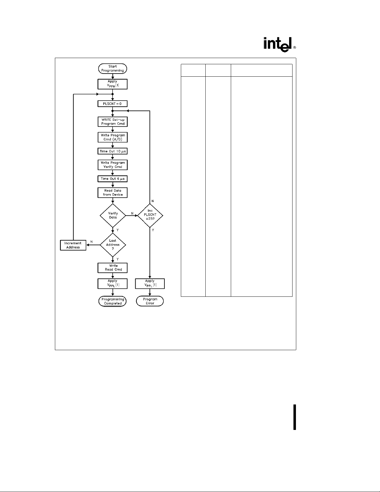
QUICK-PULSE PROGRAMMING ALGORITHM
The Quick-Pulse Programming algorithm uses pro-
gramming operations of 10 ms duration. Each opera-
tion is followed by a byte verification to determine
when the addressed byte has been successfully pro-
grammed. The algorithm allows for up to 25 pro-
gramming operations per byte, although most bytes
verify on the first or second operation. The entire
sequence of programming and byte verification is
performed with V
trates the Quick-Pulse Programming algorithm.
at high voltage. Figure 4 illus-
PP
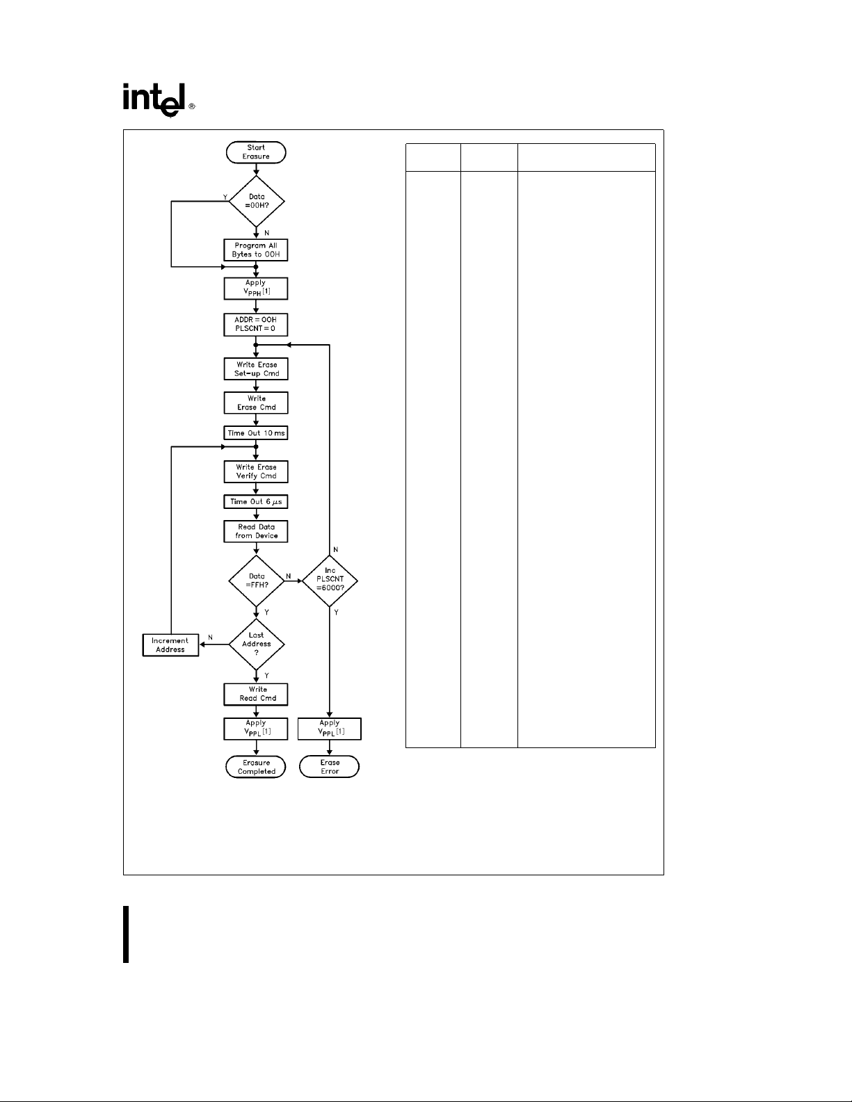
QUICK-ERASE ALGORITHM
Intel’s Quick-Erase algorithm yields fast and reliable
electrical erasure of memory contents. The algo-
rithm employs a closed-loop flow, similar to the
Quick-Pulse Programming algorithm, to simulta-
neously remove charge from all bits in the array.
Erasure begins with a read of memory contents. The
28F010 is erased when shipped from the factory.
Reading FFH data from the device would immedi-
ately be followed by device programming.
EXTENDED ERASE/PROGRAM CYCLING
EEPROM cycling failures have always concerned
users. The high electrical field required by thin oxide
EEPROMs for tunneling can literally tear apart the
oxide at defect regions. To combat this, some suppliers have implemented redundancy schemes, reducing cycling failures to insignificant levels. However, redundancy requires that cell size be doubledÐ
an expensive solution.
Intel has designed extended cycling capability into
its ETOX-II flash memory technology. Resulting improvements in cycling reliability come without increasing memory cell size or complexity. First, an
advanced tunnel oxide increases the charge carrying ability ten-fold. Second, the oxide area per cell
subjected to the tunneling electric field is one-tenth
that of common EEPROMs, minimizing the probabili-
For devices being erased and reprogrammed, uni-
form and reliable erasure is ensured by first pro-
gramming all bits in the device to their charged state
e
(Data
00H). This is accomplished, using the
Quick-Pulse Programming algorithm, in approximately two seconds.
Erase execution then continues with an initial erase
operation. Erase verification (data
e
FFH) begins at
address 0000H and continues through the array to
the last address, or until data other than FFH is encountered. With each erase operation, an increasing
number of bytes verify to the erased state. Erase
efficiency may be improved by storing the address of
the last byte verified in a register. Following the next
erase operation, verification starts at that stored address location. Erasure typically occurs in one second. Figure 5 illustrates the Quick-Erase algorithm.
9
Page 10
A28F010
Bus
Operation
Command Comments
Standby Wait for VPPRamp to V
PPH
Initialize Pulse-Count
Write Set-up Data
Program
e
40H
Write Program Valid Address/Data
Standby Duration of Program
Write Program
Verify Operation
Standby t
Read Read Byte to Verify
Standby Compare Data Output to Data
Operation (t
(3)
DataeC0H; Stops Program
WHGL
Programming
Expected
WHWH1
(2)
)
(1)
NOTES:
1. See DC Characteristics for value of V
power supply can be hard-wired to the device or
switchable. When V
ground, no-connect with a resistor tied to ground, or
less than 6.5V. Refer to Principles of Operation.
2. Refer to Principles of Operation.
is switched, V
PP
PPH
PPL
290266– 5
. The V
may be
Figure 4. 28F010 Quick-Pulse Programming Algorithm
10
Write Read Datae00H, Resets the
Standby Wait for VPPRamp to V
3. Program Verify is only performed after byte program-
PP
ming. A final read/compare may be performed (optional) after the register is written with the Read command.
4. CAUTION: The algorithm MUST BE FOLLOWED
to ensure proper and reliable operation of the device.
Register for Read Operations
PPL
(1)
Page 11
Bus
Operation
Standby Wait for V
Write Set-up Data
Command Comments
Entire Memory Muste00H
Before Erasure
Use Quick-Pulse
Programming Algorithm
(Figure 4)
PP
Initialize Addresses and
Pulse-Count
e
Erase
20H
Write Erase Datae20H
Ramp to V
A28F010
(1)
PPH
NOTES:
1. See DC Characteristics for value of V
power supply can be hard-wired to the device or
switchable. When V
ground, no-connect with a resistor tied to ground, or
less than 6.5V. Refer to Principles of Operation.
2. Refer to Principles of Operation.
is switched, V
PP
PPH
PPL
290266– 6
. The V
may be
Figure 5. A28F010 Quick-Erase Algorithm
Standby Duration of Erase Operation
Write Erase(3) Addr
Verify Data
Standby t
)
(t
WHWH2
e
Byte to Verify;
e
A0H; Stops Erase
Operation(2)
WHGL
Read Read Byte to Verify Erasure
Standby Compare Output to FFH
Write Read Datae00H, Resets the
Standby Wait for VPPRamp to V
PP
3. Erase Verify is performed only after chip-erasure. A
final read/compare may be performed (optional) after
the register is written with the read command.
4. CAUTION: The algorithm MUST BE FOLLOWED
to ensure proper and reliable operation of the device.
Increment Pulse-Count
Register for Read Operations
PPL
(1)
11
Page 12

A28F010
DESIGN CONSIDERATIONS
Two-Line Output Control
Flash-memories are often used in larger memory arrays. Intel provides two read-control inputs to accommodate multiple memory connections. Two-line
control provides for:
a. the lowest possible memory power dissipation
and,
b. complete assurance that output bus contention
will not occur.
To efficiently use these two control inputs, an address-decoder output should drive chip-enable,
while the system’s read signal controls all flashmemories and other parallel memories. This assures
that only enabled memory devices have active outputs, while deselected devices maintain the low
power standby condition.
Power Supply Decoupling
Flash memory power-switching characteristics require careful device decoupling. System designers
are interested in three supply current (I
standby, active, and transient current peaks pro-
) issuesÐ
CC
duced by falling and rising edges of chip-enable. The
capacitive and inductive loads on the device outputs
determine the magnitudes of these peaks.
Two-line control and proper decoupling capacitor
selection will suppress transient voltage peaks.
Each device should have a 0.1 mF ceramic capacitor
connected between V
and VSS.
and VSS, and between V
CC
PP
Place the high-frequency, low-inherent-inductance
capacitors as close as possible to the devices. Also,
for every eight devices, a 4.7 mF electrolytic capacitor should be placed at the array’s power supply
connection, between V
tor will overcome voltage slumps caused by printed-
and VSS. The bulk capaci-
CC
circuit-board trace inductance, and will supply
charge to the smaller capacitors as needed.
VPPTrace on Printed Circuit Boards
Programming flash-memories, while they reside in
the target system, requires that the printed circuit
board designer pay attention to the V
ply trace. The V
rent for programming. Use similar trace widths and
pin supplies the memory cell cur-
PP
layout considerations given the V
equate V
crease V
supply traces and decoupling will de-
PP
voltage spikes and overshoots.
PP
power sup-
PP
power bus. Ad-
CC
Power Up/Down Protection
The 28F010 is designed to offer protection against
accidental erasure or programming, caused by spurious system-level signals that may exist during power transitions. Also, with its control register architecture, alteration of memory contents only occurs after
successful completion of the two-step command sequences. Power supply sequencing is not required.
Internal circuitry of the 28F010 ensures that the
command register architecture is reset to the read
mode on power up.
A system designer must guard against active writes
for V
tive. Since both WE
command write, driving either to V
writes. The control register architecture provides an
voltages above the V
CC
Ý
and CEÝmust be low for a
will prohibit
IH
when VPPis ac-
LKO
added level of protection since alteration of memory
contents only occurs after successful completion of
the two-step command sequences.
28F010 Power Dissipation
When designing portable systems, designers must
consider battery power consumption not only during
device operation, but also for data retention during
system idle time. Flash nonvolatility increases the
usable battery life of your system because the
28F010 does not consume any power to retain code
or data when the system is off. Table 4 illustrates the
power dissipated when updating the 28F010.
Table 4. 28F010 Typical Update
Power Dissipation
Operation
Power Dissipation
(Watt-Seconds)
Array Program/ 0.171 1
Program Verify
Array Erase/ 0.136 2
Erase Verify
One Complete 0.478 3
Cycle
NOTES:
1. Formula to calculate typical Program/Program Verify
e
Power
(t
WHWH1
c
Ý
BytesctypicalÝProg Pulses (t
a
t
cal
WHGL
2. Formula to calculate typical Erase/Erase Verify Power
e
[
V
PP(VPP3
c
t
WHGL
c
I
typicalct
CC5
3. One Complete Cycle
a
Erase
4. ‘‘Typicals’’ are not guaranteed, but based on a limited
number of samples from production lots.
[
V
PP
c
I
PP2
c
typicalct
Ý
Bytes)
Program.
c
Ý
BytesctypicalÝProg Pulses
typicalat
I
CC4
WHGL
a
]
typical].
[
V
CC(ICC3
c
WHGL
ERASE
Ý
e
(4)
Notes
c
I
PP4
WHWH1
typicalaI
typicalct
Bytes)].
Array PreprogramaArray
typical)
PP5
ERASE
c
a
]
I
CC2
typical
typical
[
V
typi-
CC
c
12
Page 13
A28F010
ABSOLUTE MAXIMUM RATINGS*
Operating Temperature
During Read АААААААААААААА
During Erase/Program АААААААb40§Ctoa125§C
Temperature Under BiasААААААААb40§Ctoa125§C
Storage Temperature ААААААААААb65§Ctoa150§C
Voltage on Any Pin with
Respect to Ground АААААААААА
Voltage on Pin A9with
Respect to Ground ААААААА
VPPSupply Voltage with
Respect to Ground
During Erase/Program ÀÀÀÀ
NOTES:
1. Operating temperature is for automotive product defined by this specification.
2. Minimum DC input voltage is
Maximum DC voltage on output pins is V
3. Maximum DC voltage on A
4. Output shorted for no more than one second. No more than one output shorted at a time.
b
40§Ctoa125§C
b
2.0V toa7.0V
b
2.0V toa13.5V
b
2.0V toa14.0V
b
0.5V. During transitions, inputs may undershoot tob2.0V for periods less than 20 ns.
a
or VPPmay overshoot toa14.0V for periods less than 20 ns.
9
CC
(2, 3)
(2, 3)
0.5V, which may overshoot to V
VCCSupply Voltage with
Respect to Ground АААААААААА
Output Short Circuit CurrentААААААААААААА100 mA
(1)
Maximum Junction Temperature (TJ) ААААААa140§C
NOTICE: This is a production data sheet. The specifications are subject to change without notice.
*
WARNING: Stressing the device beyond the ‘‘Absolute
(2)
Maximum Ratings’’ may cause permanent damage.
These are stress ratings only. Operation beyond the
‘‘Operating Conditions’’ is not recommended and extended exposure beyond the ‘‘Operating Conditions’’
may affect device reliability.
a
2.0V for periods less than 20 ns.
CC
OPERATING CONDITIONS
Symbol Parameter
Limits
Unit Comments
Min Max
T
A
V
CC
Operating Temperature
VCCSupply Voltage 4.50 5.50 V
b
40
a
125
C For Read-Only and
§
b
2.0V toa7.0V
Read/Write Operations
(2)
(4)
DC CHARACTERISTICSÐTTL/NMOS COMPATIBLE
Symbol Parameter Notes
I
I
I
I
I
I
I
I
I
I
Input Leakage Current 1
LI
Output Leakage Current 1
LO
VCCStandby Current 1 1.0 mA V
CCS
VCCActive Read Current 1 10 30 mA V
CC1
VCCProgramming Current 1, 2 1.0 30 mA Programming in Progress
CC2
VCCErase Current 1, 2 5.0 30 mA Erasure in Progress
CC3
VCCProgram Verify Current 1, 2 5.0 30 mA V
CC4
VCCErase Verify Current 1, 2 5.0 30 mA V
CC5
VPPLeakage Current 1
PPS
VPPRead Current or 1 90 200 mAV
PP1
Standby Current
Limits
Min Typical Max
g
1.0 mAV
g
10 m AV
g
10 m AV
g
10 m AV
Unit Test Conditions
e
VCCMax
CC
e
V
VCCor V
IN
e
VCCMax
CC
e
V
CE
OUT
CC
Ý
CC
e
e
e
VCCor V
VCCMax
V
IH
VCCMax, CE
fe6 MHz, I
e
V
PP
PPH
e
V
PP
PPH
s
V
PP
CC
l
V
PP
CC
s
V
PP
CC
SS
SS
e
Ý
V
OUT
e
IL
0mA
Program Verify in Progress
Erase Verify in Progress
13
Page 14
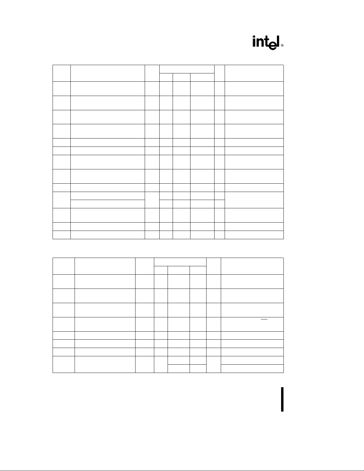
A28F010
DC CHARACTERISTICSÐTTL/NMOS COMPATIBLE (Continued)
Symbol Parameter Notes
I
I
I
I
V
V
V
V
V
I
VPPProgramming Current 1, 2 8.0 30 mA V
PP2
VPPErase Current 1, 2 4.0 30 mA V
PP3
VPPProgram Verify Current 1, 2 2.0 5.0 mA V
PP4
VPPErase Verify Current 1, 2 2.0 5.0 mA V
PP5
Input Low Voltage
IL
Input High Voltage 2.0 V
IH
Output Low Voltage 0.45 V I
OL
Output High Voltage 2.4 V I
OH1
A9Intelligent Identifer Voltage 11.50 13.00 V A
ID
VCCID Current
ID
1
VPPID CURRENT 90 500 mA
V
PPLVPP
V
PPHVPP
V
LKOVCC
during Read-Only Operations 0.00 6.5 V NOTE: Erase/Program are
during Read/Write Operations 11.40 12.60 V
Erase/Write Lock Voltage 2.5 V
b
Limits
Min Typical Max
0.5 0.8 V
a
0.5 V
CC
10 30 mA
Unit Test Conditions
e
V
PP
PPH
Programming in Progress
e
V
PP
PPH
Erasure in Progress
e
V
PP
PPH
Program Verify in Progress
e
V
PP
PPH
Erase Verify in Progress
e
2.1 mA
OL
e
V
VCCMin
CC
eb
CC
9
9
e
e
e
2.5 mA
VCCMin
V
ID
V
ID
PP
e
V
PPL
OH
V
A
Inhibited when V
DC CHARACTERISTICSÐCMOS COMPATIBLE
Symbol Parameter Notes
I
LI
I
LO
I
CCS
I
CC1
I
CC2
I
CC3
I
PPS
I
PP1
Input Leakage Current 1
Output Leakage Current 1
VCCStandby Current 1 300 mAV
VCCActive Read Current 1 10 30 mA V
VCCProgramming Current 1, 2 1.0 30 mA Programming in Progress
VCCErase Current 1, 2 5.0 30 mA Erasure in Progress
VPPLeakage Current 1
VPPRead Current or 1 90 200 mAV
Standby Current
14
Limits
Min Typical Max
Unit Test Conditions
g
1.0 mAV
g
10 mAV
V
V
CE
CC
IN
CC
OUT
CC
Ý
CC
e
fe6 MHz, I
g
10 mAV
g
10 V
PP
PP
PP
e
VCCMax
VCCor V
e
e
e
e
e
s
V
l
V
s
V
SS
VCCMax
VCCor V
VCCMax
g
V
0.2V
CC
VCCMax, CEeV
e
OUT
CC
CC
CC
SS
IL
0mA
Page 15
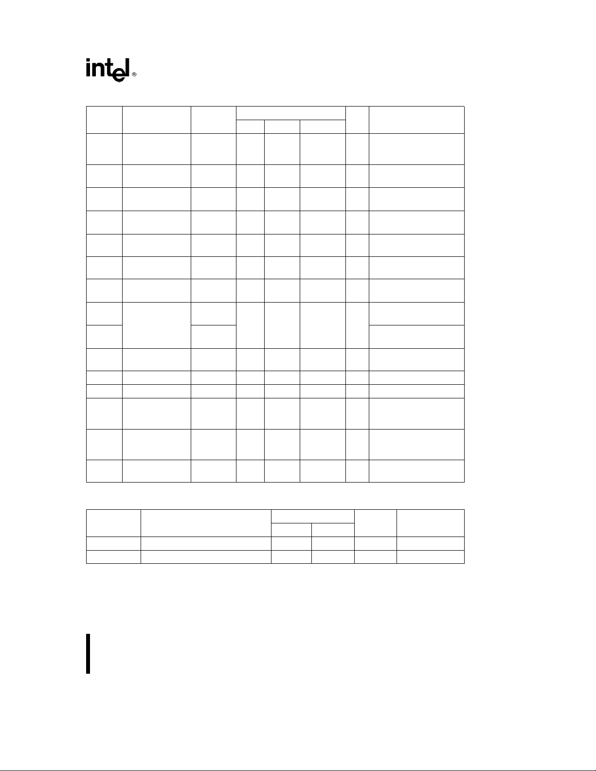
DC CHARACTERISTICSÐCMOS COMPATIBLE (Continued)
Symbol Parameter Notes
I
PP2
V
PP
Programming
1, 2 8.0 30 mA V
Current
I
I
I
V
V
V
V
V
V
I
I
V
V
PP3
PP4
PP5
IL
IH
OL
OH1
OH2
ID
ID
ID
PPL
PPH
VPPErase 1, 2 4.0 30 mA V
Current
VPPProgram 1, 2 2.0 5.0 mA V
Verify Current
VPPErase Verify 1, 2 5.0 5.0 mA V
Current
Input Low
b
0.5 0.8 V
Voltage
Input High 0.7 V
Voltage
Output Low 0.45 V I
Voltage
Output High 0.85 V
Voltage
b
V
CC
A9Intelligent 11.50 13.00 V
Identifier Voltage
VCCID Current 1 10 30 mA A
VPPID Current 1 90 500 mAA
VPPduring Read- 0.00 6.5 V NOTE: Erase/Programs
Only Operations are Inhibited when
VPPduring 11.40 12.60 V
Read/Write
Operations
V
LKO
VCCErase/Write 2.5 V
Lock Voltage
Min Typical Max
CC
CC
0.4 I
Limits
a
V
0.5 V
CC
A28F010
Unit Test Conditions
e
V
PP
OL
OH
OH
PP
PP
PP
CC
CC
CC
9
9
PP
e
e
e
e
e
eb
e
eb
e
e
e
e
PPH
V
PPH
V
PPH
V
PPH
2.1 mA
VCCMin
2.5 mA,
VCCMin
100 mA,
VCCMin
ID
ID
V
PPL
Program
Programming in Progress
Erasure in Progress
Verify in Progress
Erase Verify in Progress
V
I
V
V
V
V
(3)
CAPACITANCE
Symbol Parameter
e
T
25§C, fe1.0 MHz
A
Limits
Unit Conditions
Min Max
C
IN
C
OUT
NOTES:
1. All currents are in RMS unless otherwise noted. Typical values at V
2. Not 100% tested: characterization data available.
3. Sampled, not 100% tested.
4. ‘‘Typicals’’ are not guaranteed, but are based on a limited number of samples from production lots.
Address/Control Capacitance 8 pF V
Output Capacitance 12 pF V
CC
e
5.0V, V
e
12.0V, Te25§C.
PP
IN
OUT
e
0V
e
0V
15
Page 16
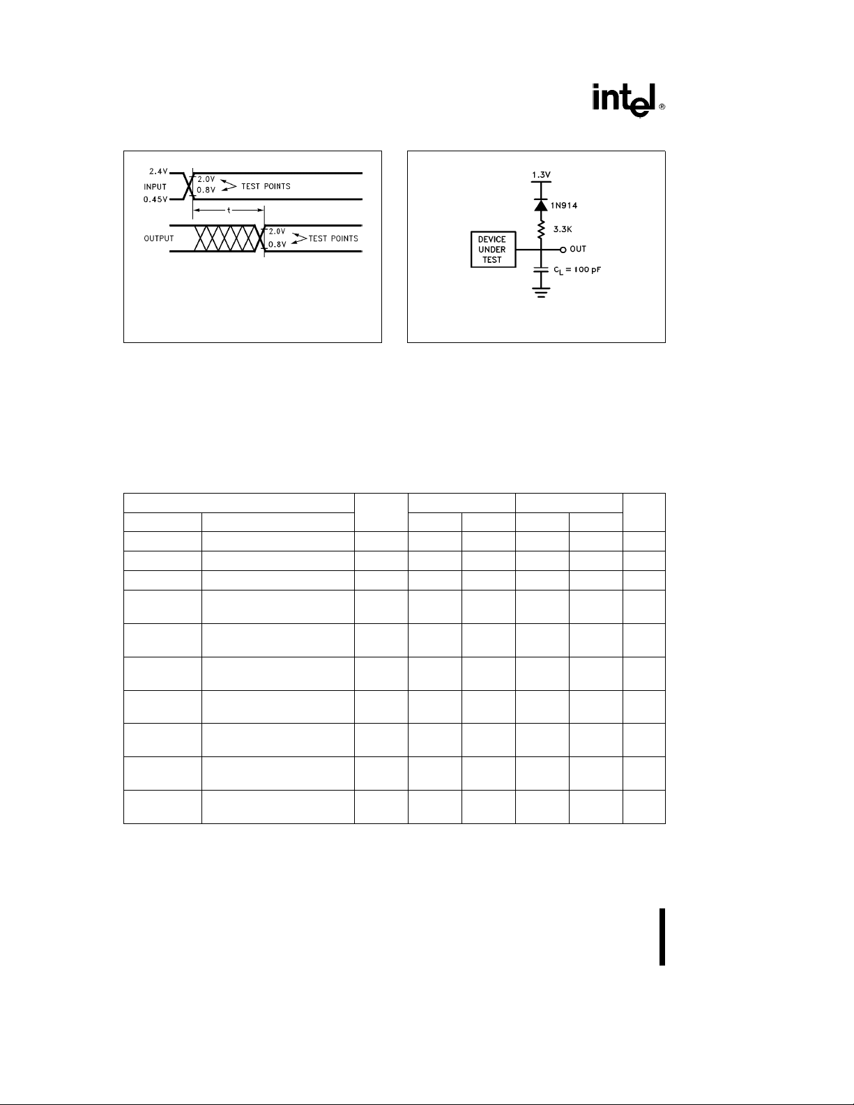
A28F010
AC TESTING INPUT/OUTPUT WAVEFORM
290266– 7
AC Testing: Inputs are driven at 2.4V for a logic ‘‘1’’ and 0.45V for
a logic ‘‘0’’. Testing measurements are made at 2.0V for a logic
‘‘1’’ and 0.8V for a logic ‘‘0’’. Rise/Fall time
s
10 ns.
AC TESTING LOAD CIRCUIT
e
C
100 pF
L
includes Jig Capacitance
C
L
AC TEST CONDITIONS
Input Rise and Fall Times (10% to 90%) АААААА10 ns
Input Pulse Levels АААААААААААААААА0.45V and 2.4V
Input Timing Reference Level ААААААА0.8V and 2.0V
Output Timing Reference Level АААААА0.8V and 2.0V
AC CHARACTERISTICSÐRead-Only Operations
Versions
Symbol Characteristic Min Max Min Max
t
AVAV/tRC
t
ELQV/tCE
t
AVQV/tACC
t
GLQV/tOE
Read Cycle Time 3 120 150 ns
Chip Enable Access Time 120 150 ns
Address Access Time 120 150 ns
Output Enable 50 55 ns
Notes
(2)
28F010-120 28F010-150
Access Time
t
ELQX/tLZ
Chip Enable to 3 0 0 ns
Output in Low Z
t
EHQZ
Chip Disable to 3 55 55 ns
Output in High Z
t
GLQX/tOLZ
Output Enable to 3 0 0 ns
Output in Low Z
t
GHQZ/tDF
Output Disable to 4 30 35 ns
Output in High Z
t
OH
t
WHGL
Output Hold from Address, 1, 3 0 0 ns
Ý
CE
,orOEÝChange
Write Recovery Time 6 6 ms
before Read
290266– 8
Unit
NOTES:
1. Whichever occurs first.
2. Rise/Fall Time
3. Not 100% tested: characterization data available.
4. Guaranteed by design.
s
10 ns.
16
Page 17
A28F010
290266– 9
Figure 6. AC Waveforms for Read Operations
17
Page 18
A28F010
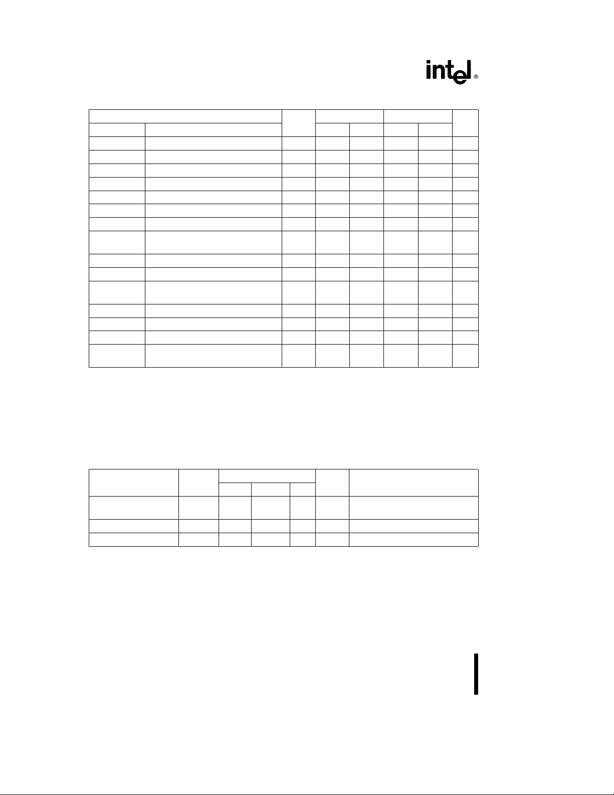
AC CHARACTERISTICSÐWrite/Erase/Program Operations
Versions
Notes
Symbol Characteristic Min Max Min Max
t
AVAV/tWC
t
AVWL/tAS
t
WLAX/tAH
t
DVWH/tDS
t
WHDX/tDH
t
WHGL
t
GHWL
t
ELWL/tCS
t
WHEH/tCH
t
WLWH/tWP
t
ELEH
t
WHWL/tWPH
t
WHWH1
t
WHWH2
t
VPEL
NOTES:
1. Read timing characteristics during read/write operations are the same as during read-only operations. Refer to AC Characteristics for Read-Only Operations.
2. Chip-Enable Controlled Writes: Write operations are driven by the valid combination of Chip-Enable and Write-Enable. In
systems where Chip-Enable defines the write pulse width (within a longer Write-Enable timing waveform) all set-up, hold, and
inactive Write-Enable times should be measured relative to the Chip-Enable waveform.
3. Rise/Fall time
4. The internal stop timer terminates the programming/erase operations, thereby eliminating the need for a maximum specification.
Write Cycle Time 120 150 ns
Address Set-Up Time 0 0 ns
Address Hold Time 2 60 60 ns
Data Set-up Time 50 50 ns
Data Hold Time 10 10 ns
Write Recovery Time before Read 6 6 ms
Read Recovery Time before Write 0 0 ms
Chip Enable 2 20 20 ns
Set-Up Time before Write
Chip Enable Hold Time 0 0 ns
(2)
(2)
280 80 ns
280 80 ns
Write Pulse Width
Alternative Write
Pulse Width
Write Pulse Width High 20 20 ns
Duration of Programming Operation 4 10 10 ms
Duration of Erase Operation 4 9.5 9.5 ms
VPPSet-Up 1.0 1.0 ms
Time to Chip Enable Low
s
10 ns.
28F010-120 28F010-150
(1, 3)
Unit
ERASE AND PROGRAMMING PERFORMANCE
Parameter Notes
Limits
Unit Comments
Min Typ Max
Chip Erase Time 1, 3, 4, 6 1 60 Sec Excludes 00H Programming
Prior to Erasure
Chip Program Time 1, 2, 4 2 12.5 Sec Excludes System-Level Overhead
Erase/Program Cycles 1, 5 1,000 100,000 Cycles
NOTES:
1. ‘‘Typicals’’ are not guaranteed, but based on a limited number of samples taken from production lots. Data taken at
e
25§C, V
T
2. Minimum byte programming time excluding system overhead is 16 msec (10 msec program
while maximum is 400 msec/byte (16 msec x 25 loops allowed by algorithm). Max chip programming time is specified lower
than the worst case allowed by the programming algorithm since most bytes program significantly faster than the worst case
byte.
3. Excludes 00H programming prior to erasure.
4. Excludes system-level overhead.
5. Refer to RR-60 ‘‘ETOX Flash Memory Reliability Data Summary’’ for typical cycling data and failure rate calculations.
6. Maximum erase specification is determined by algorithmic limit and accounts for cumulative effect of erasure at
eb
T
e
12.0V, V
PP
40§C, 1,000 cycles, V
CC
e
5.0V.
e
11.4V, V
PP
CC
e
4.5V.
a
6 msec write recovery),
18
Page 19
A28F010
290266– 17
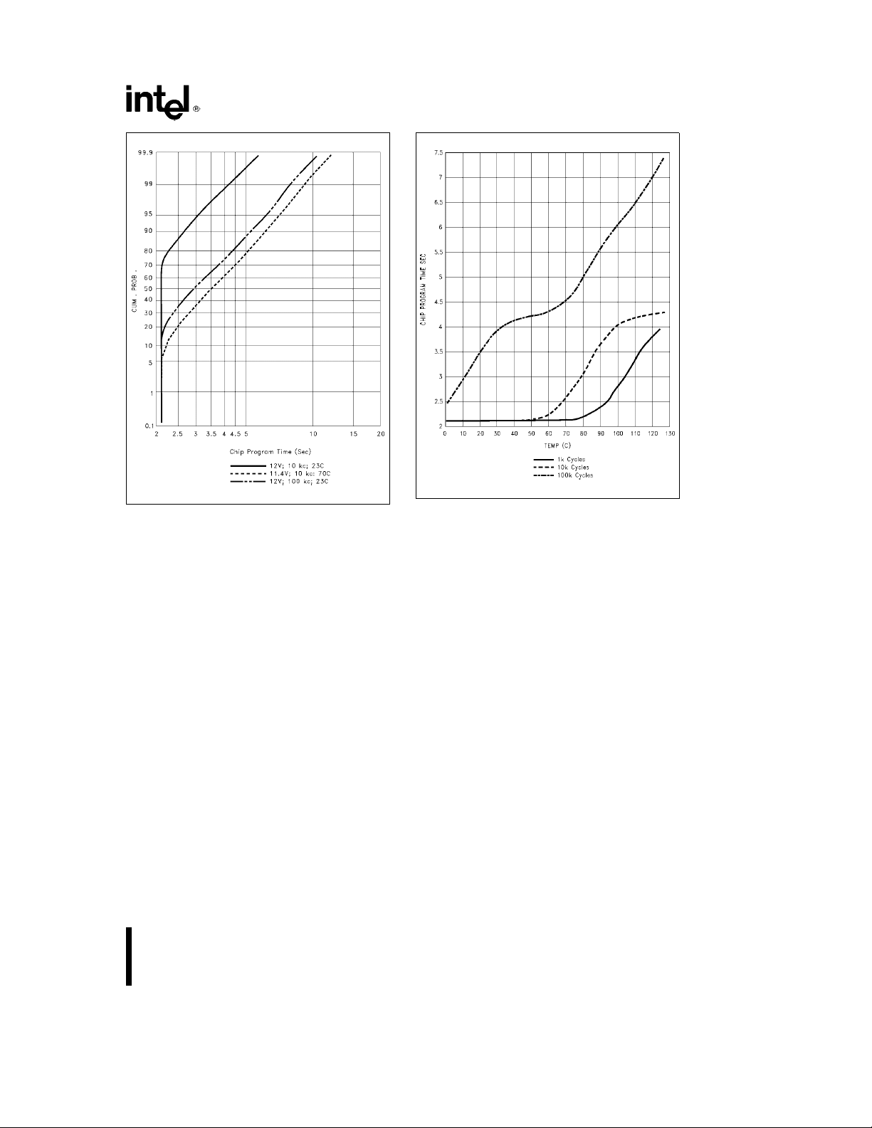
Figure 7. 28F010 Typical Programming Capability
See Note 1, Page 18.
290266– 18
Figure 8. 28F010 Typical Program Time at 12V
19
Page 20
A28F010
290266– 19
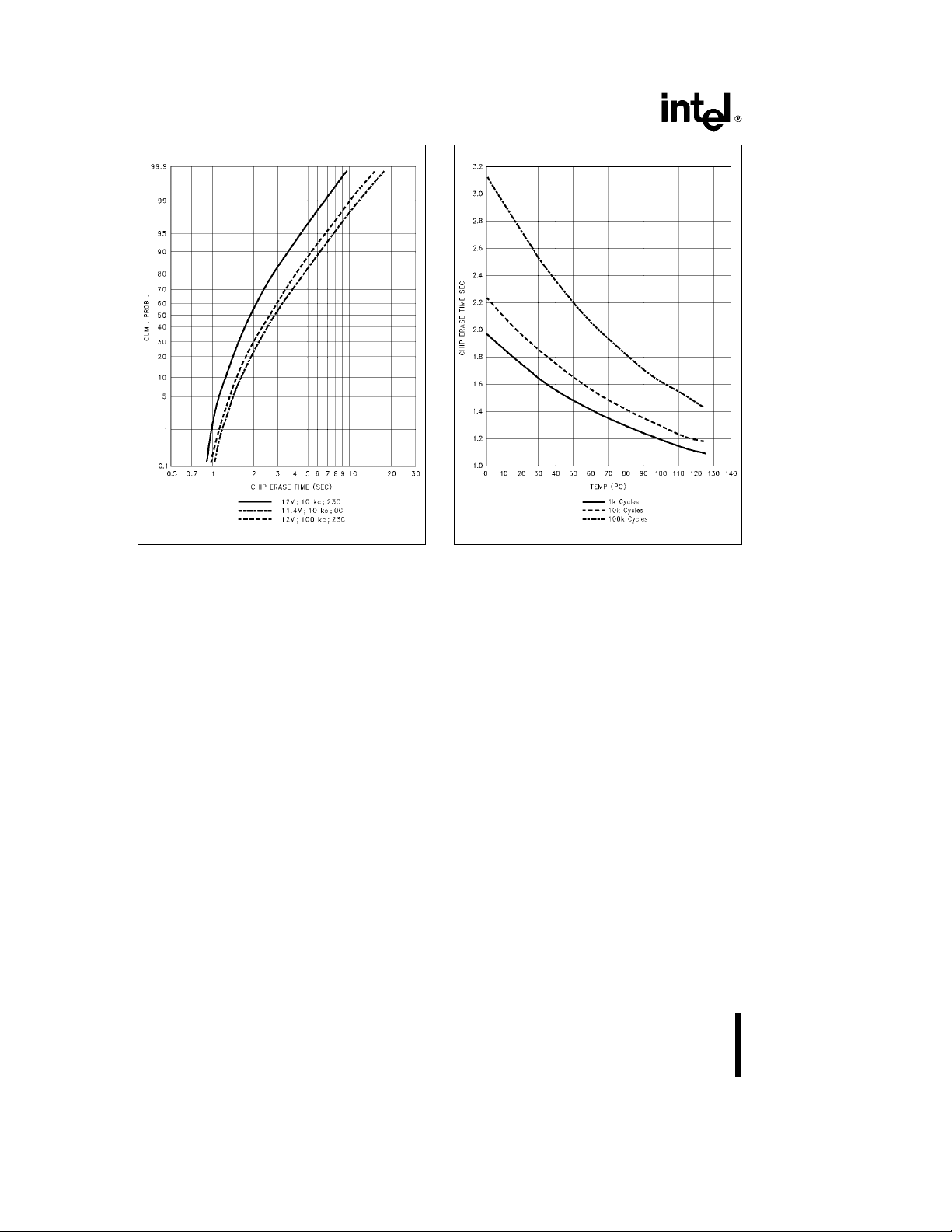
Figure 9. 28F010 Typical Erase Capability
See Note 1, Page 18.
290266– 20
Figure 10. 28F010 Typical Erase Time at 12V
20
Page 21
A28F010
290266– 14
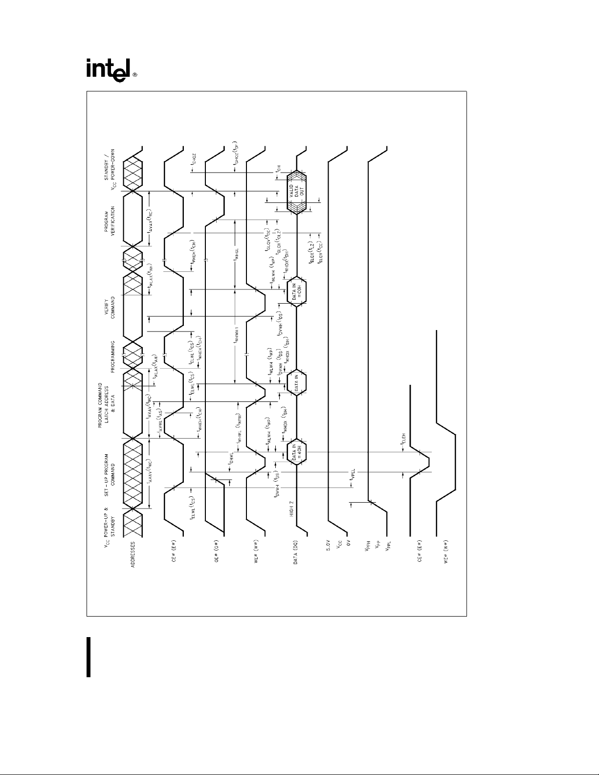
Figure 11. AC Waveforms for Programming Operations
Alternative Write Timing
21
Page 22
A28F010
290266– 15
22
Figure 12. AC Waveforms for Erase Operations
Page 23
A28F010
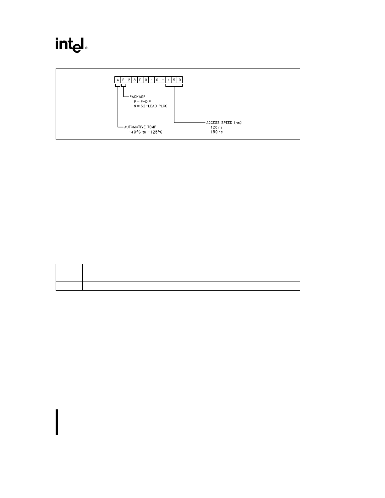
Ordering Information
290266– 16
Valid Combinations:
AP28F010-120
AP28F010-150
AN28F010-120
AN28F010-150
ADDITIONAL INFORMATION Order Number
ER-20, ‘‘ETOXTMII Flash Memory Technology’’ 294005
ER-24, ‘‘Intel Flash Memory’’ 294008
RR-60, ‘‘ETOX
TM
Flash Memory Reliability Data Summary’’ 293002
AP-316, ‘‘Using Flash Memory for In-System Reprogrammable 292046
AP-325, ‘‘Guide to Flash Memory Reprogramming’’ 292059
Nonvolatile Storage’’
REVISION HISTORY
Number Description
003 Changed Erase/Program Cycles to 1,000 minimum
004 Added 120 ns Characteristics
23
 Loading...