

Page 1
FEATURES
MX27C4100/27C4096
4M-BIT [512K x 8/256K x 16] CMOS EPROM
• 256K x 16 organization(MX27C4096, JEDEC pin
out)
• 512K x 8 or 256K x 16 organization(MX27C4100,
ROM pin out compatible)
• +12.5V programming voltage
• Fast access time: 100/120/150 ns
• Totally static operation
GENERAL DESCRIPTION
The MX27C4100/4096 is a 5V only, 4M-bit, One Time
Programmable Read Only Memory. It is organized as
256K words by 16 bits per word(MX27C4096), 512K x 8
or 256K x 16(MX27C4100), operates from a single + 5
volt supply, has a static standby mode, and features fast
single address location programming. All programming
signals are TTL levels, requiring a single pulse. For
programming outside from the system, existing EPROM
PIN CONFIGURATIONS
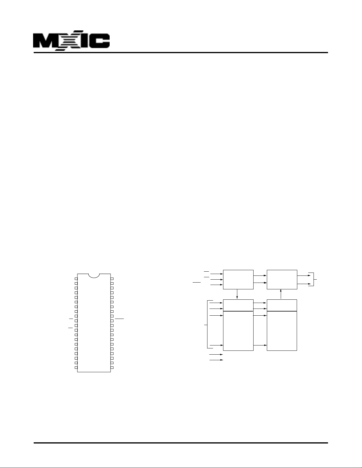
SOP/PDIP(MX27C4100)
• Completely TTL compatible
• Operating current: 60mA
• Standby current: 100uA
• Package type:
- 40 pin plastic DIP
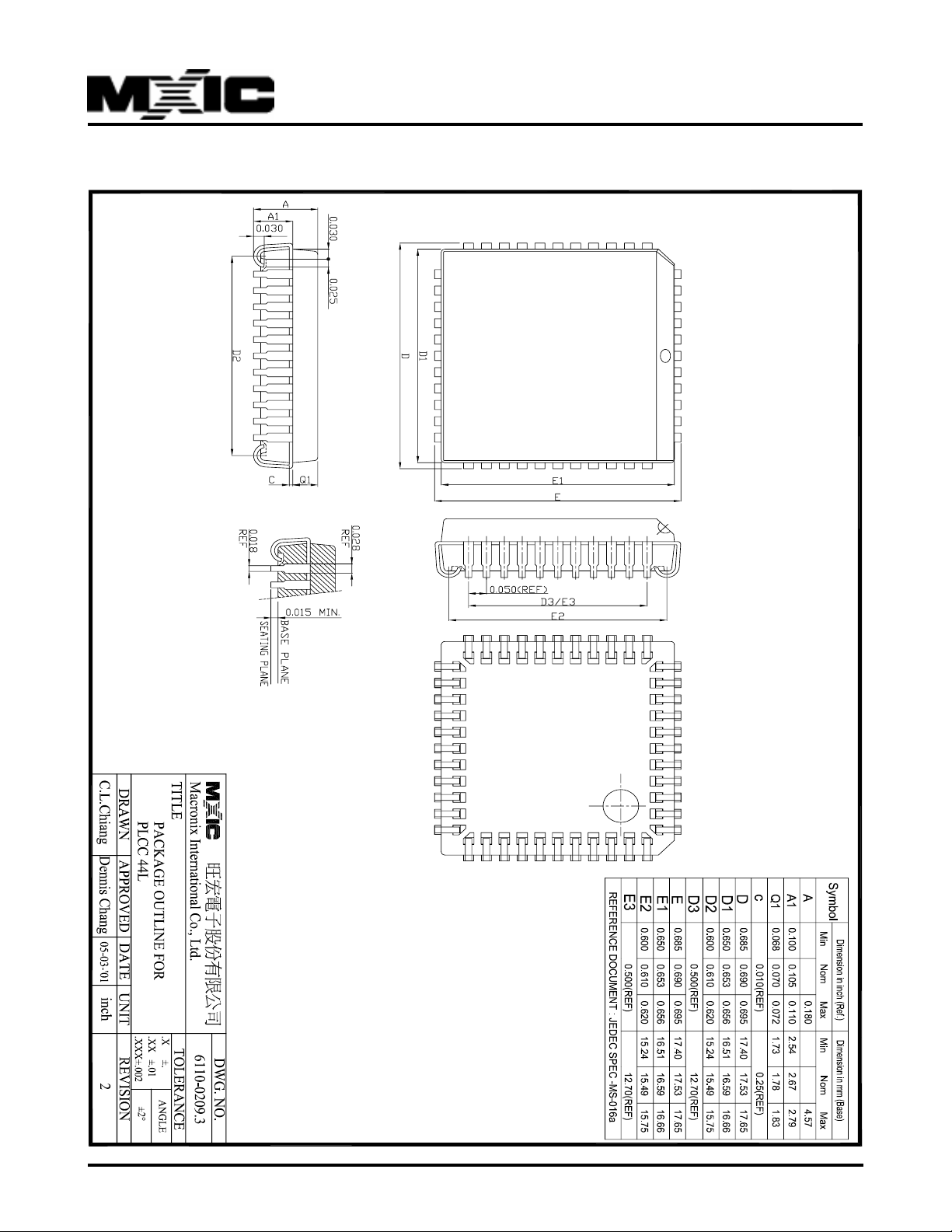
- 44 pin PLCC
- 40 pin SOP
programmers may be used. The MX27C4100/4096
supports a intelligent fast programming algorithm which
can result in programming time of less than two minutes.
This EPROM is packaged in industry standard 40 pin
dual-in-line packages, 40 lead SOP, and 44 lead PLCC
packages.
BLOCK DIAGRAM (MX27C4100)
A17
CE
GND
OE
Q0
Q8
Q1
Q9
Q2
Q10
Q3
Q11
1
2
A7
3
A6
4
A5
5
A4
6
A3
7
A2
8
A1
9
A0
10
11
12
13
14
15
16
17
18
19
20
40
A8
39
A9
38
A10
37
A11
36
A12
35
A13
34
A14
33
A15
32
A16
31
BYTE/VPP
30
GND
29
MX27C4100
Q15/A-1
28
Q7
27
Q14
26
Q6
25
Q13
24
Q5
23
Q12
22
Q4
21
VCC
CE
OE
BYTE/VPP
A0~A17
ADDRESS
INPUTS
VCC
GND
.
.
.
.
.
.
.
.
CONTROL
LOGIC
Y-DECODER
X-DECODER
OUTPUT
BUFFERS
.
Y-SELECT
.
.
.
4M BIT
.
.
.
.
CELL
MAXTRIX
Q0~Q14
Q15/A-1
P/N: PM0197
1
REV. 3.4, AUG. 22, 2001
Page 2
MX27C4100/27C4096
PIN CONFIGURATIONS
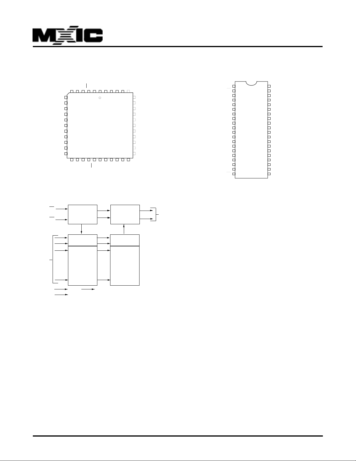
PLCC(MX27C4096)
Q13
Q14
Q15CEVPPNCVCC
64440
7
Q12
Q11
Q10
Q9
Q8
12
GND
NC
Q7
Q6
Q5
17
Q4
18 23 28
Q3Q2Q1
MX27C4096
Q0
OE
1
NC
A17
A16
A15
A0A1A2A3A4
BLOCK DIAGRAM (MX27C4096)
CE
OE
CONTROL
LOGIC
OUTPUT
BUFFERS
PIN CONFIGURATIONS
PDIP(MX27C4096)
1
A14
A13
39
A12
A11
A10
A9
GND
34
NC
A8
A7
A6
A5
29
Q0~Q15
VPP
CE
Q15
Q14
Q13
Q12
Q11
Q10
Q9
Q8
GND
Q7
Q6
Q5
Q4
Q3
Q2
Q1
Q0
OE
2
3
4
5
6
7
8
9
10
11
12
13
14
15
16
17
18
19
20
40
VCC
39
A17
38
A16
37
A15
36
A14
35
A13
34
A12
33
A11
32
A10
31
A9
30
GND
29
MX27C4096
A8
28
A7
27
A6
26
A5
25
A4
24
A3
23
A2
22
A1
21
A0
A0~A17
ADDRESS
INPUTS
VCC
GND
.
.
.
.
.
.
.
.
Y-DECODER
X-DECODER
VPP
.
Y-SELECT
.
.
.
4M BIT
.
.
.
.
CELL
MAXTRIX
P/N: PM0197
2
REV. 3.4, AUG. 22, 2001
Page 3
MX27C4100/27C4096
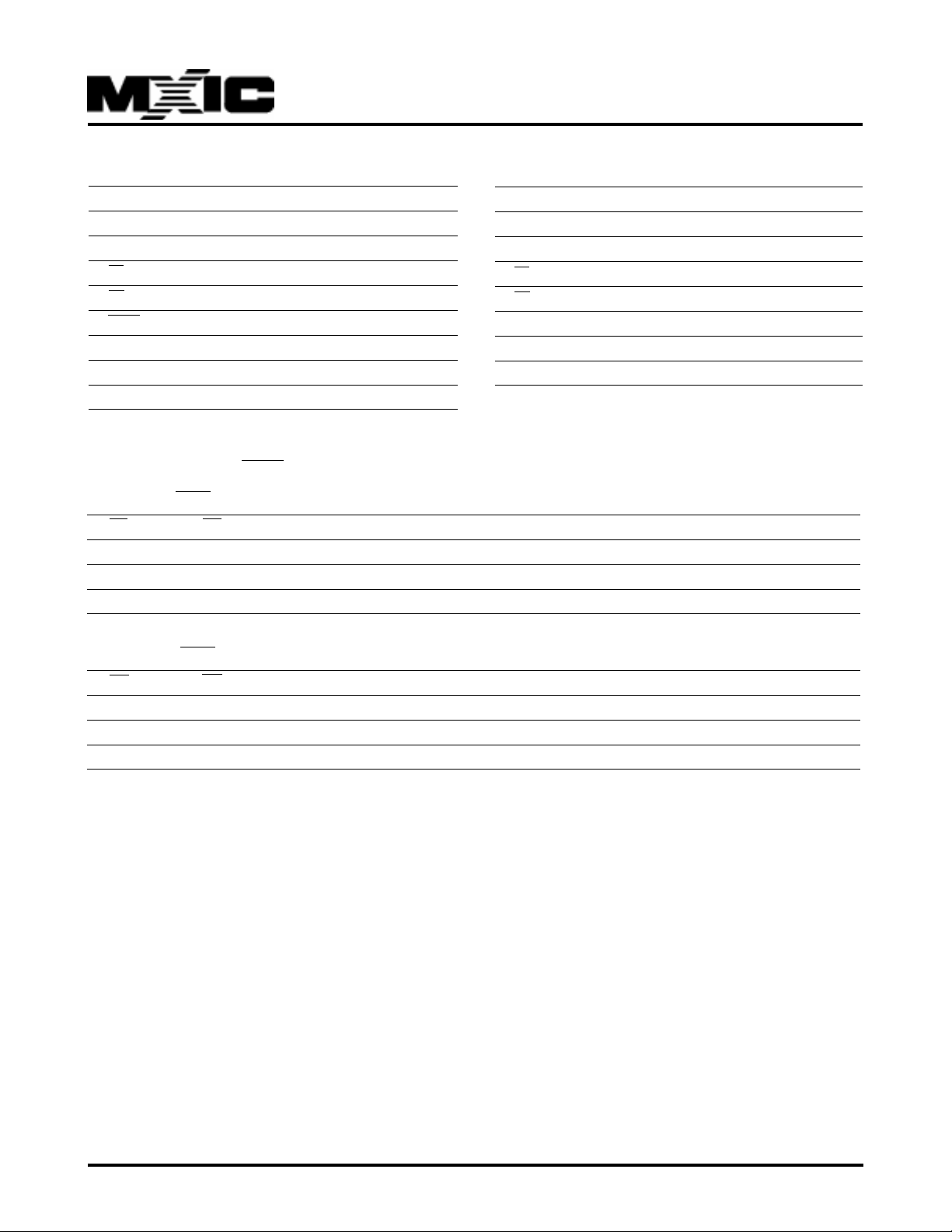
PIN DESCRIPTION(MX27C4100)
SYMBOL PIN NAME
A0~A17 Address Input
Q0~Q14 Data Input/Output
CE Chip Enable Input
OE Output Enable Input
BYTE/VPP Word/Byte Selection/Program Supply Voltage
Q15/A-1 Q15(Word mode)/LSB addr. (Byte mode)
VCC Power Supply Pin (+5V)
GND Ground Pin
PIN DESCRIPTION(MX27C4096)
SYMBOL PIN NAME
A0~A17 Address Input
Q0~Q15 Data Input/Output
CE Chip Enable Input
OE Output Enable Input
VPP Program Supply Voltage
VCC Power Supply Pin (+5V)
GND Ground Pin
TRUTH TABLE OF BYTE FUNCTION(MX27C4100)
BYTE MODE(BYTE = GND)
CE OE Q15/A-1 MODE Q0-Q7 SUPPLY CURRENT
H X X Non selected High Z Standby(ICC2)
L H X Non selected High Z Operating(ICC1)
L L A-1 input Selected DOUT Operating(ICC1)
WORD MODE(BYTE = VCC)
CE OE Q15/A-1 MODE Q0-Q14 SUPPLY CURRENT
H X High Z Non selected High Z Standby(ICC2)
L H High Z Non selected High Z Operating(ICC1)
L L DOUT Selected DOUT Operating(ICC1)
NOTE : X = H or L
P/N: PM0197
3
REV. 3.4, AUG. 22, 2001
Page 4

MX27C4100/27C4096
FUNCTIONAL DESCRIPTION
THE PROGRAMMING OF THE MX27C4100/4096
When the MX27C4100/4096 is delivered, or it is
erased, the chip has all 4M bits in the "ONE" or HIGH
state. "ZEROs" are loaded into the MX27C4100/4096
through the procedure of programming.
For programming, the data to be programmed is applied
with 16 bits in parallel to the data pins.
VCC must be applied simultaneously or before VPP,
and removed simultaneously or after VPP. When
programming an MXIC EPROM, a 0.1uF capacitor is
required across VPP and ground to suppress spurious
voltage transients which may damage the device.
FAST PROGRAMMING
The device is set up in the fast programming mode when
the programming voltage VPP = 12.75V is applied, with
VCC = 6.25 V and OE = VIH (Algorithm is shown in
Figure 1). The programming is achieved by applying a
single TTL low level 100us pulse to the CE input after
addresses and data line are stable. If the data is not
verified, an additional pulse is applied for a maximum of
25 pulses. This process is repeated while sequencing
through each address of the device. When the
programming mode is completed, the data in all address
is verified at VCC = VPP = 5V ± 10%.
The verification should be performed with OE and CE at
VIL(for MX27C4096), OE at VIL and CE at VIH(for
MX27C4100) and VPP at its programming voltage.
AUTO IDENTIFY MODE
The auto identify mode allows the reading out of a binary
code from an EPROM that will identify its manufacturer
and device type. This mode is intended for use by
programming equipment for the purpose of
automatically matching the device to be programmed
with its corresponding programming algorithm. This
mode is functional in the 25°C± 5°C ambient
temperature range that is required when programming
the MX27C4100/4096.
To activate this mode, the programming equipment
must force 12.0 ± 0.5 V on address line A9 of the device.
Two identifier bytes may then be sequenced from the
device outputs by toggling address line A0 from VIL to
VIH. All other address lines must be held at VIL during
auto identify mode.
Byte 0 ( A0 = VIL) represents the manufacturer code,
and byte 1 (A0 = VIH), the device identifier code. For the
MX27C4100/4096, these two identifier bytes are given
in the Mode Select Table. All identifiers for manufacturer
and device codes will possess odd parity, with the MSB
(Q15) defined as the parity bit.
READ MODE
PROGRAM INHIBIT MODE
Programming of multiple MX27C4100/4096's in parallel
with different data is also easily accomplished by using
the Program Inhibit Mode. Except for CE and OE, all like
inputs of the parallel MX27C4100/4096 may be
common. A TTL low-level program pulse applied to an
MX27C4100/4096 CE input with VPP = 12.5 ± 0.5 V will
program the MX27C4100/4096. A high-level CE input
inhibits the other MX27C4100/4096s from being
programmed.
PROGRAM VERIFY MODE
Verification should be performed on the programmed
bits to determine that they were correctly programmed.
P/N: PM0197
The MX27C4100/4096 has two control functions, both of
which must be logically satisfied in order to obtain data
at the outputs. Chip Enable (CE) is the power control
and should be used for device selection. Output Enable
(OE) is the output control and should be used to gate
data to the output pins, independent of device selection.
Assuming that addresses are stable, address access
time (tACC) is equal to the delay from CE to output (tCE).
Data is available at the outputs tOE after the falling edge
of OE's, assuming that CE has been LOW and
addresses have been stable for at least tACC - t OE.
WORD-WIDE MODE
With BYTE/VPP at VCC ± 0.2V outputs Q0-7 present
data Q0-7 and outputs Q8-15 present data Q8-15, after
CE and OE are appropriately enabled.
REV. 3.4, AUG. 22, 2001
4
Page 5

MX27C4100/27C4096
BYTE-WIDE MODE
With BYTE/VPP at GND ± 0.2V, outputs Q8-15 are tristated. If Q15/A-1 = VIH, outputs Q0-7 present data bits
Q8-15. If Q15/A-1 = VIL, outputs Q0-7 present data bits
Q0-7.
STANDBY MODE
The MX27C4100/4096 has a CMOS standby mode
which reduces the maximum VCC current to 100 uA. It
is placed in CMOS standby when CE is at VCC ± 0.3 V.
The MX27C4100/4096 also has a TTL-standby mode
which reduces the maximum VCC current to 1.5 mA. It
is placed in TTL-standby when CE is at VIH. When in
standby mode, the outputs are in a high-impedance
state, independent of the OE input.
TWO-LINE OUTPUT CONTROL FUNCTION
To accommodate multiple memory connections, a twoline control function is provided to allow for:
used between VCC and GND for each eight devices.
The location of the capacitor should be close to where
the power supply is connected to the array.
1. Low memory power dissipation,
2. Assurance that output bus contention will not
occur.
It is recommended that CE be decoded and used as the
primary device-selecting function, while OE be made a
common connection to all devices in the array and
connected to the READ line from the system control bus.
This assures that all deselected memory devices are in
their low-power standby mode and that the output pins
are only active when data is desired from a particular
memory device.
SYSTEM CONSIDERATIONS
During the switch between active and standby
conditions, transient current peaks are produced on the
rising and falling edges of Chip Enable. The magnitude
of these transient current peaks is dependent on the
output capacitance loading of the device. At a minimum,
a 0.1 uF ceramic capacitor (high frequency, low inherent
inductance) should be used on each device between
Vcc and GND to minimize transient effects. In addition,
to overcome the voltage drop caused by the inductive
effects of the printed circuit board traces on EPROM
arrays, a 4.7 uF bulk electrolytic capacitor should be
P/N: PM0197
5
REV. 3.4, AUG. 22, 2001
Page 6
MX27C4100/27C4096
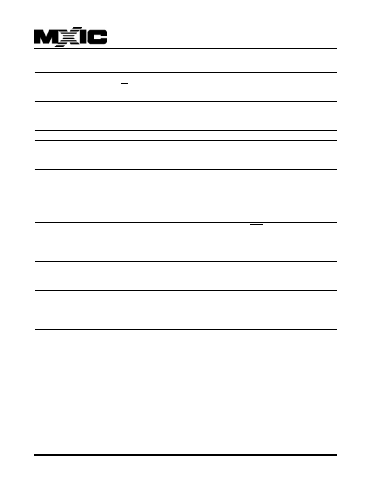
MODE SELECT TABLE (MX27C4096)
PINS
MODE CE OE A0 A9 VPP OUTPUTS
Read VIL VIL X X VCC DOUT
Output Disable VIL VIH X X VCC High Z
Standby (TTL) VIH X X X VCC High Z
Standby (CMOS) VCC±0.3V X X X VCC High Z
Program VIL VIH X X VPP DIN
Program Verify VIH VIL X X VPP DOUT
Program Inhibit VIH VIH X X VPP High Z
Manufacturer Code(3) VIL VIL VIL VH VCC 00C2H
Device Code(3) VIL VIL VIH VH VCC 0151H
NOTES: 1. VH = 12.0 V ± 0.5 V
2. X = Either VIH or VIL
3. A1 - A8 = A10 - A17 = VIL(For auto select)
4. See DC Programming Characteristics for VPP voltage during
programming.
MODE SELECT TABLE (MX27C4100)
BYTE/
MODE CE OE A9 A0 Q15/A-1 VPP(5) Q8-14 Q0-7
Read (Word) VIL VIL X X Q15 Out VCC Q8-14 Out Q0-7 Out
Read (Upper Byte) VIL VIL X X VIH GND High Z Q8-15 Out
Read (Lower Byte) VIL VIL X X VIL GND High Z Q0-7 Out
Output Disable VIL VIH X X High Z X High Z High Z
Standby VIH X X X High Z X High Z High Z
Program VIL VIH X X Q15 In VPP Q8-14 In Q0-7 In
Program Verify VIH VIL X X Q15 Out VPP Q8-14 Out Q0-7 Out
Program Inhibit VIH VIH X X High Z VPP High Z High Z
Manufacturer Code(3) VIL VIL VH VIL 0B VCC 00H C2H
Device Code(3) VIL VIL VH VIH 1B VCC 38H 00H
NOTES: 1. VH = 12.0V ± 0.5V
2. X = Either VIH or VIL
3. A1 - A8, A10 - A17 = VIL(for auto select)
4. See DC Programming Characteristics for VPP voltages.
5. BYTE/VPP is intended for operation under DC Voltage conditions
only.
6. Manufacture code = 00C2H
Device code = B800H
P/N: PM0197
6
REV. 3.4, AUG. 22, 2001
Page 7
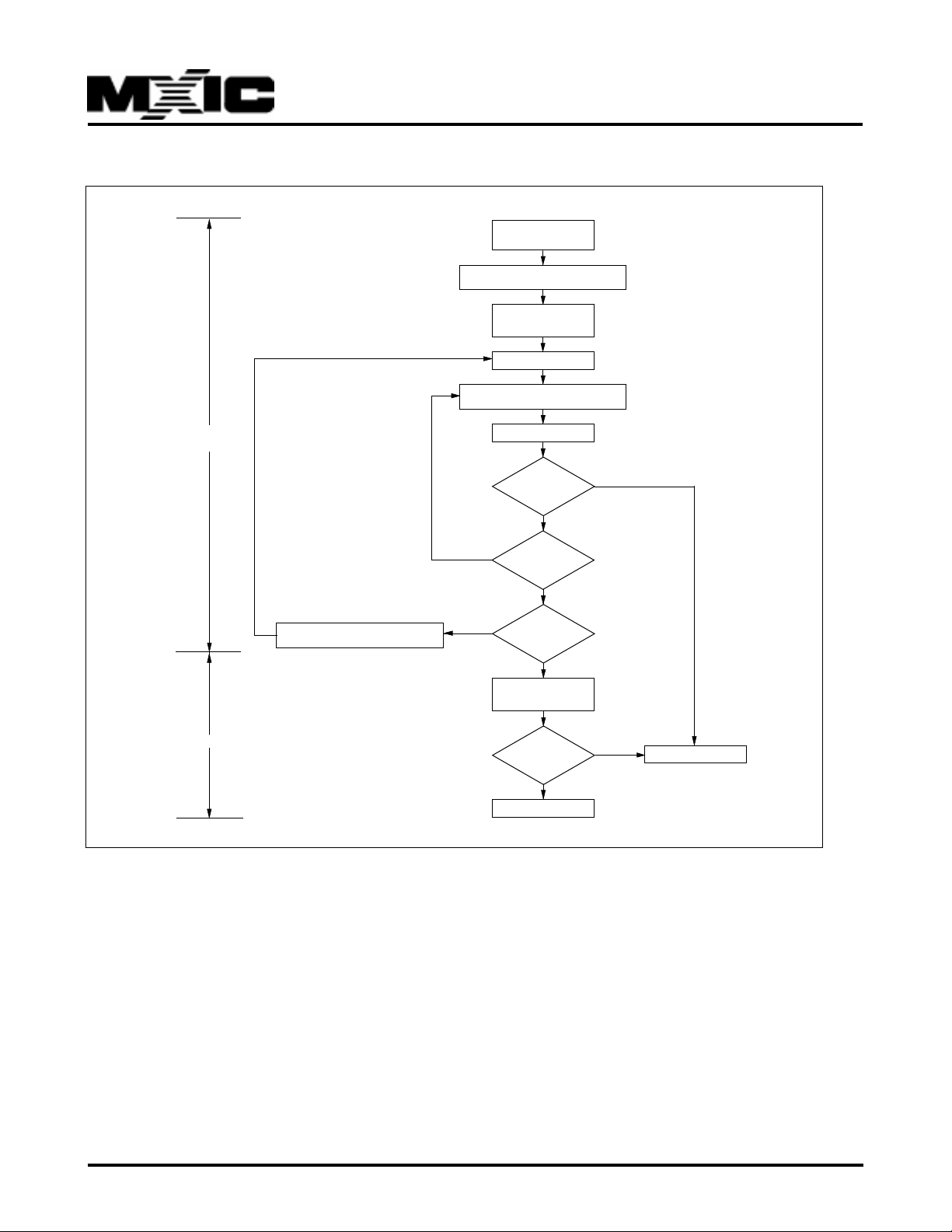
FIGURE 1. FAST PROGRAMMING FLOW CHART
MX27C4100/27C4096
START
ADDRESS = FIRST LOCATION
VCC = 6.25V
VPP = 12.75V
X = 0
PROGRAM ONE 100us PULSE
INTERACTIVE
SECTION
VERIFY SECTION
INCREMENT ADDRESS
FAIL
NO
INCREMENT X
X = 25?
NO
VERIFY BYTE
?
PASS
LAST ADDRESS
YES
VCC = VPP = 5.25V
VERIFY ALL BYTES
?
PASS
DEVICE PASSED
YES
FAIL
FAIL
DEVICE FAILED
P/N: PM0197
7
REV. 3.4, AUG. 22, 2001
Page 8
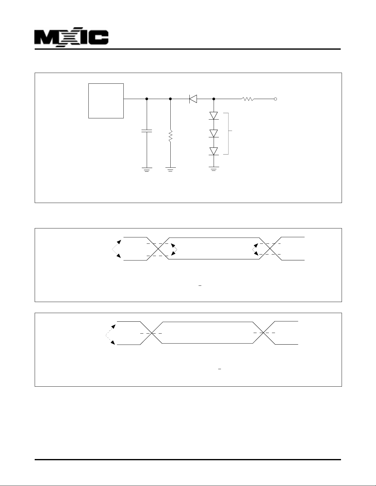
SWITCHING TEST CIRCUITS
MX27C4100/27C4096
DEVICE
UNDER
TEST
CL = 100 pF including jig capacitance(30pF for 100 ns parts)
SWITCHING TEST WAVEFORMS
AC driving levels
AC TESTING:
AC driving levels are 2.4V/0.4V for commercial grade , 3.0V/0V for industrial grade.
Input pulse rise and fall times are <10ns.
CL
INPUT
6.2K ohm
2.0V
0.8V
TEST POINTS
1.8K ohm
DIODES = IN3064
OR EQUIVALENT
2.0V
0.8V
OUTPUT
+5V
P/N: PM0197
AC driving levels
1.5V
INPUT
AC TESTING: (1)AC driving levels are 3.0V/0V for both commercial grade and industrial grade.
Input pulse rise and fall times are < 10ns.
(2)For MX27C4100/4096-10
TEST POINTS
OUTPUT
8
1.5V
REV. 3.4, AUG. 22, 2001
Page 9
MX27C4100/27C4096
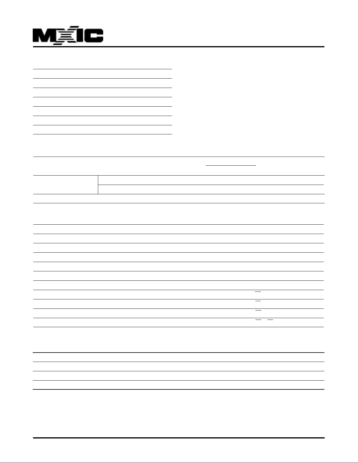
ABSOLUTE MAXIMUM RATINGS
RATING VALUE
Ambient Operating Temperature -40oC to 85oC
Storage Temperature -65oC to 125oC
Applied Input Voltage -0.5V to 7.0V
Applied Output Voltage -0.5V to VCC + 0.5V
VCC to Ground Potential -0.5V to 7.0V
A9 & VPP -0.5V to 13.5V
NOTICE:
Stresses greater than those listed under ABSOLUTE MAXIMUM
RATINGS may cause permanent damage to the device. This is a
stress rating only and functional operation of the device at these or
any other conditions above those indicated in the operational
sections of this specification is not implied. Exposure to absolute
maximum rating conditions for extended period may affect reliability.
NOTICE:
Specifications contained within the following tables are subject to
change.
DC/AC Operating Conditions for Read Operation
MX27C4100/4096
-10 -12 -15
Operating Temperature Commercial 0°C to 70°C0°C to 70°C0°C to 70°C
Industrial -40°C to 85°C -40°C to 85°C -40°C to 85°C
Vcc Power Supply 5V ± 5% 5V ± 10% 5V ± 10%
DC CHARACTERISTICS
SYMBOL PARAMETER MIN. MAX. UNIT CONDITIONS
VOH Output High Voltage 2.4 V IOH = -0.4mA
VOL Output Low Voltage 0.4 V IOL = 2.1mA
VIH Input High Voltage 2.0 VCC + 0.5 V
VIL Input Low Voltage -0.3 0.8 V
ILI Input Leakage Current -10 10 uA VIN = 0 to 5.5V
ILO Output Leakage Current -10 10 uA VOUT = 0 to 5.5V
ICC3 VCC Power-Down Current 100 uA CE = VCC ± 0.3V
ICC2 VCC Standby Current 1.5 mA CE = VIH
ICC1 VCC Active Current 60 mA CE = VIL, f=5MHz, Iout = 0mA
IPP VPP Supply Current Read 10 uA CE = OE = VIL, VPP = 5.5V
CAPACITANCE TA = 25
SYMBOL PARAMETER TYP. MAX. UNIT CONDITIONS
CIN Input Capacitance 8 12 pF VIN = 0V
COUT Output Capacitance 8 12 pF VOUT = 0V
CVPP VPP Capacitance 18 25 pF VPP = 0V
P/N: PM0197
o
C, f = 1.0 MHz (Sampled only)
9
REV. 3.4, AUG. 22, 2001
Page 10
MX27C4100/27C4096
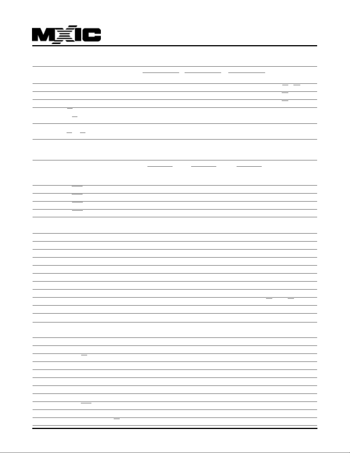
AC CHARACTERISTICS
27C4100/4096-10 27C4100/4096-12 27C4100/4096-15
SYMBOL PARAMETER MIN. MAX. MIN. MAX. MIN. MAX. UNIT CONDITIONS
tACC Address to Output Delay 100 120 150 ns CE = OE = VIL
tCE Chip Enable to Output Delay 100 120 150 n s OE = VIL
tOE Output Enable to Output Delay 45 50 65 ns CE = VIL
tDF OE High to Output Float, 0 30 0 35 0 50 ns
or CE High to Output Float
tOH Output Hold from Address, 0 0 0 ns
CE or OE which ever occurred first
AC CHARACTERISTICS(Continued)
27C4100-10 27C4100-12 27C4100-15
SYMBOL PARAMETER MIN. MAX. MIN. MAX. MIN. MAX. UNIT
CONDITIONS
tBHA BYTE Access Time 100 120 150 ns
tOHB BYTE Output Hold Time 0 0 0 ns
tBHZ BYTE Output Delay Time 70 70 70 ns
tBLZ BYTE Output Set Time 10 10 10 ns
DC PROGRAMMING CHARACTERISTICS TA = 25
SYMBOL PARAMETER MIN. MAX. UNIT CONDITIONS
VOH Output High Voltage 2.4 V IOH = -0.40mA
VOL Output Low Voltage 0.4 V IOL = 2.1mA
VIH Input High Voltage 2.0 VCC + 0.5 V
VIL Input Low Voltage -0.3 0.8 V
ILI Input Leakage Current -10 10 uA VIN = 0 to 5.5V
VH A9 Auto Select Voltage 11.5 12.5 V
ICC3 VCC Supply Current (Program & Verify) 50 mA
IPP2 VPP Supply Current(Program) 30 mA CE = VIL, OE = VIH
VCC1 Fast Programming Supply Voltage 6.00 6.50 V
VPP1 Fast Programming Voltage 12.5 13.0 V
AC PROGRAMMING CHARACTERISTICS TA = 25
SYMBOL PARAMETER MIN. MAX. UNIT CONDITIONS
tAS Address Setup Time 2.0 us
tOES OE Setup Time 2.0 us
tDS Data Setup Time 2.0 us
tAH Address Hold Time 0 us
tDH Data Hold Time 2.0 us
tDFP Output Enable to Output Float Delay 0 130 ns
tVPS VPP Setup Time 2.0 us
tPW PGM Program Pulse Width 95 105 us
tVCS VCC Setup Time 2.0 us
tOE Data valid from OE 150 ns
o
C ± 5°C
o
C ± 5°C
P/N: PM0197
10
REV. 3.4, AUG. 22, 2001
Page 11
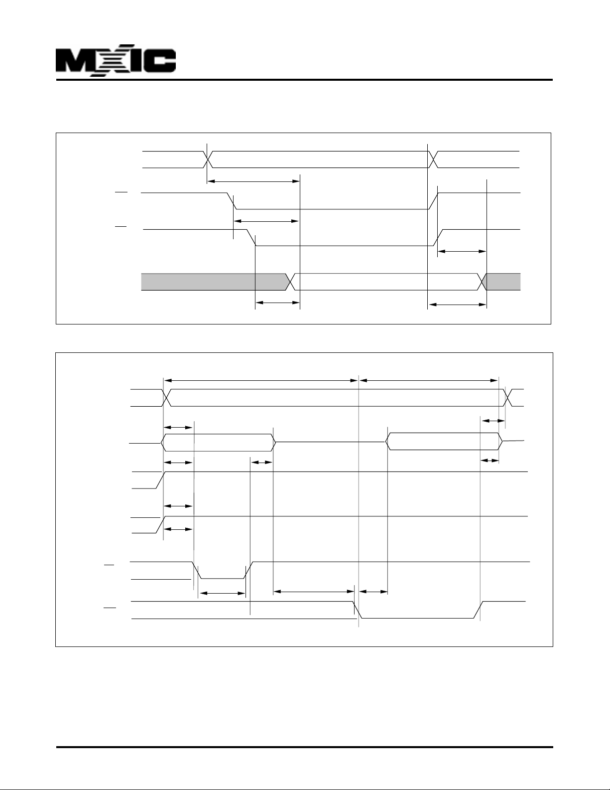
WEFORMS(MX27C4096)
READ CYCLE(WORD MODE)
MX27C4100/27C4096
ADDRESS
INPUTS
tACC
CE
tCE
OE
DATA
OUT
tOE
FAST PROGRAMMING ALGORITHM WAVEFORMS
PROGRAM
tDH
Addresses
DATA
VIH
VIL
tAS
DATA IN STABLE
tDS
VPP1
DATA ADDRESS
VALID DATA
Hi-z
tDF
tOH
PROGRAM VERIFY
tAH
DATA OUT VALID
tDFP
P/N: PM0197
VPP
VCC
CE
OE
VCC
VCC1
VCC
VIH
VIL
VIH
VIL
tVPS
tVCS
tPW
11
tOES
tOE
Max
REV. 3.4, AUG. 22, 2001
Page 12
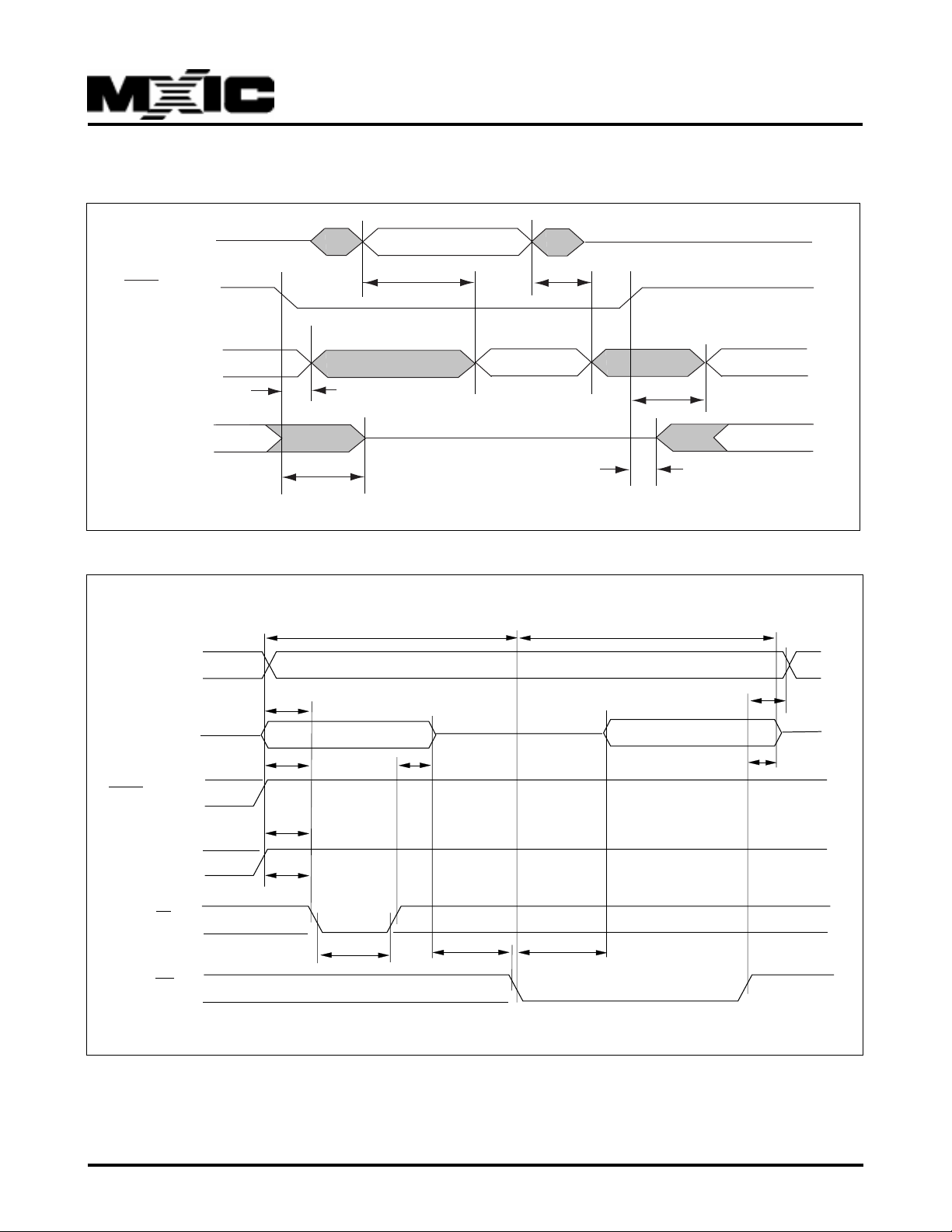
WAVEFORMS(MX27C4100)
READ CYCLE (BYTE MODE)
MX27C4100/27C4096
A-1
HIGH-Z
tACC
BYTE/VPP
Q0-Q7
tOHB
Q15-Q8
tBHZ
FAST PROGRAMMING ALGORITHM WAVEFORMS
PROGRAM
Addresses
VIH
VIL
tAS
VALID DATA
VALID ADDRESS
HIGH-Z
tOH
VALID DATA
tBHA
VALID DATA
tBLZ
VERIFY
tAH
BYTE/VPP
P/N: PM0197
DATA
VCC
CE
OE
VPP1
VCC
VCC1
VCC
VIH
VIL
VIH
VIL
tDS
tVPS
tVCS
DATA SET
tPW
tDH
tOES
12
DATA OUT VALID
tDFP
tOE
REV. 3.4, AUG. 22, 2001
Page 13
MX27C4100/27C4096
ORDERING INFORMATION
PLASTIC PACKAGE
PART NO. ACCESS TIME OPERATING STANDBY OPERATING PACKAGE
(ns) CURRENT MAX.(mA) CURRENT MAX.(uA) TEMPERATURE
MX27C4100PC-10 100 60 100 0°C to 70°C 40 Pin DIP(ROM pin out)
MX27C4100PC-12 120 60 100 0°C to 70°C 40 Pin DIP(ROM pin out)
MX27C4100PC-15 150 60 100 0°C to 70°C 40 Pin DIP(ROM pin out)
MX27C4100MC-10 100 60 100 0°C to 70°C 40 Pin SOP(ROM pin out)
MX27C4100MC-12 120 60 100 0°C to 70°C 40 Pin SOP(ROM pin out)
MX27C4100MC-15 150 60 100 0°C to 70°C 40 Pin SOP(ROM pin out)
MX27C4096PC-10 100 60 100 0°C to 70°C 40 Pin DIP(JEDEC pin out)
MX27C4096PC-12 120 60 100 0°C to 70°C 40 Pin DIP(JEDEC pin out)
MX27C4096PC-15 150 60 100 0°C to 70°C 40 Pin DIP(JEDEC pin out)
MX27C4096QC-10 100 60 100 0°C to 70°C 44 Pin PLCC
MX27C4096QC-12 120 60 100 0°C to 70°C 44 Pin PLCC
MX27C4096QC-15 150 60 100 0°C to 70°C 44 Pin PLCC
MX27C4100PI-10 100 60 100 -40°C to 85°C 40 Pin DIP(ROM pin out)
MX27C4100PI-12 120 60 100 -40°C to 85°C 40 Pin DIP(ROM pin out)
MX27C4100PI-15 150 60 100 -40°C to 85°C 40 Pin DIP(ROM pin out)
MX27C4100MI-10 100 60 100 -40 °C to 85°C 40 Pin SOP(ROM pin out)
MX27C4100MI-12 120 60 100 -40 °C to 85°C 40 Pin SOP(ROM pin out)
MX27C4100MI-15 150 60 100 -40 °C to 85°C 40 Pin SOP(ROM pin out)
MX27C4096PI-10 100 60 100 --40°C to 85°C 40 Pin DIP(JEDEC pin out)
MX27C4096PI-12 120 60 100 -40°C to 85°C 40 Pin DIP(JEDEC pin out)
MX27C4096PI-15 150 60 100 -40°C to 85°C 40 Pin DIP(JEDEC pin out)
MX27C4096QI-10 100 60 100 -40°C to 85°C 44 Pin PLCC
MX27C4096QI-12 120 60 100 -40°C to 85°C 44 Pin PLCC
MX27C4096QI-15 150 60 100 -40°C to 85°C 44 Pin PLCC
P/N: PM0197
13
REV. 3.4, AUG. 22, 2001
Page 14
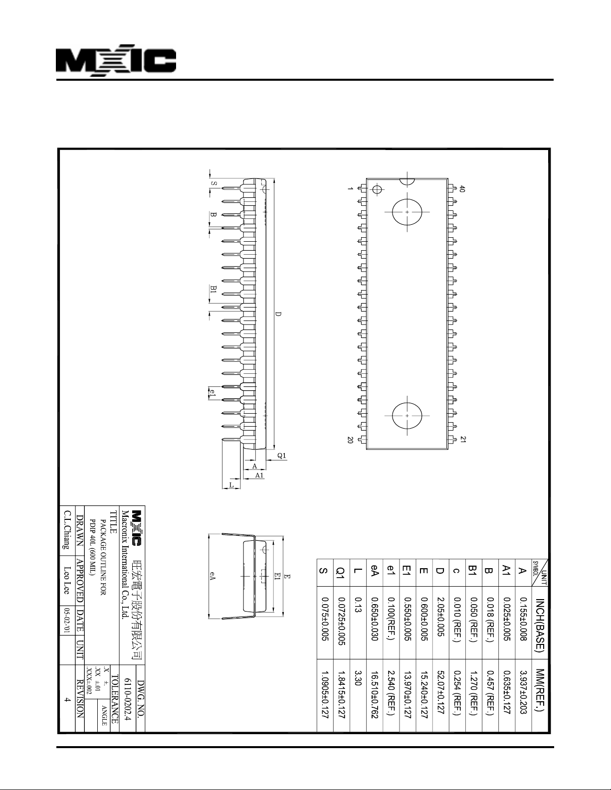
PACKAGE INFORMATION
40-PIN PLASTIC DIP(600 mil)
MX27C4100/27C4096
P/N: PM0197
14
REV. 3.4, AUG. 22, 2001
Page 15
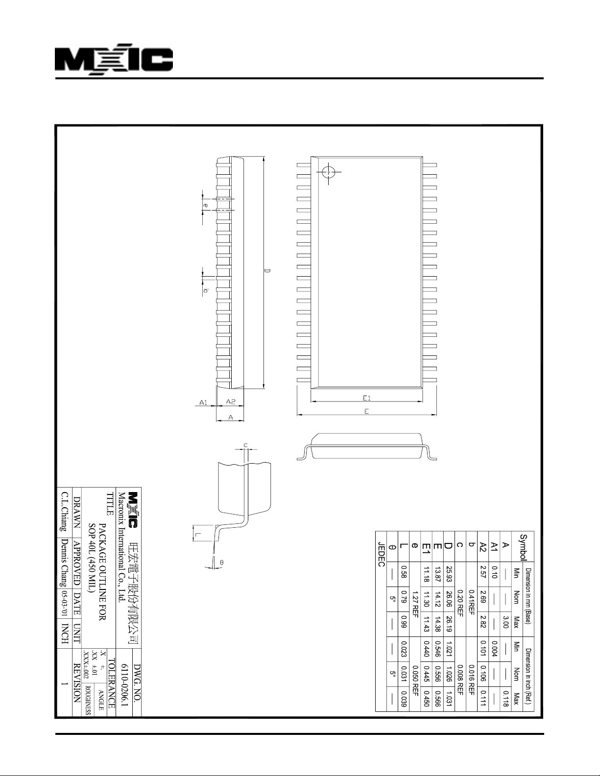
40-PIN PLASTIC SOP(450 mil)
MX27C4100/27C4096
P/N: PM0197
15
REV. 3.4, AUG. 22, 2001
Page 16
MX27C4100/27C4096
44-PIN PLASTIC LEADED CHIP CARRIER(PLCC)
P/N: PM0197
16
REV. 3.4, AUG. 22, 2001
Page 17

MX27C4100/27C4096
Revision History
Revision No. Description Pgae Date
3.0 1) Eliminate Interactive Programming Mode 6/13/1997
2) 40-CDIP package quartz lens, change to square shape.
3.1 IPP1 100uA to 10uA 7/17/1997
3.2 Cancel 32pin ceramic DIP Package P1,2,4,13,14 FEB/25/2000
3.3 Modify Commercial range 0~55°C-->0~70°C P9 MAY/03/2000
3.4 Cancel "Ultraviolet Erasable" wording in General Description P1 AUG/22/2001
To modify Package Information P14~16
P/N: PM0197
17
REV. 3.4, AUG. 22, 2001
Page 18

MX27C4100/27C4096
MACRONIX INTERNATIONAL CO., LTD.
HEADQUARTERS:
TEL:+886-3-578-6688
FAX:+886-3-563-2888
EUROPE OFFICE:
TEL:+32-2-456-8020
FAX:+32-2-456-8021
JAPAN OFFICE:
TEL:+81-44-246-9100
FAX:+81-44-246-9105
SINGAPORE OFFICE:
TEL:+65-348-8385
FAX:+65-348-8096
TAIPEI OFFICE:
TEL:+886-2-2509-3300
FAX:+886-2-2509-2200
MACRONIX AMERICA, INC.
TEL:+1-408-453-8088
FAX:+1-408-453-8488
CHICAGO OFFICE:
TEL:+1-847-963-1900
FAX:+1-847-963-1909
http : //www.macronix.com
MACRONIX INTERNATIONAL CO., LTD. reserves the right to change product and specifications without notice.
18
 Loading...