

Page 1
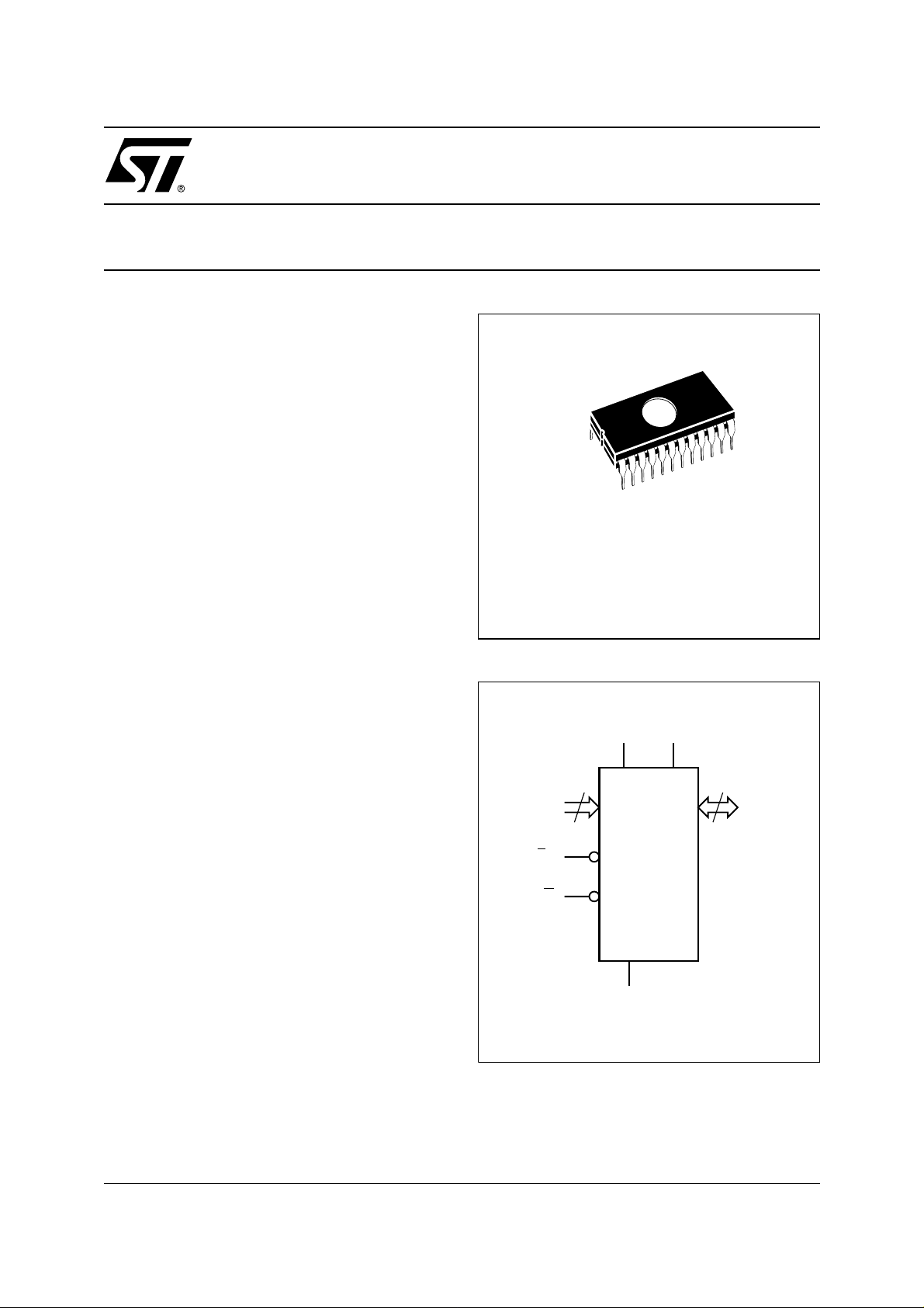
NMOS 16 Kbit (2Kb x 8) UV EPROM
■ 2048 x 8 ORGANIZATION
■ 525mW Max ACTIVE POWER, 132mW Ma x
STANDBY POWER
■ ACCESS TIME:
– M2716-1 is 350ns
– M2716 is 450ns
■ SINGLE 5V SUPPLY VOLTAGE
■ STATIC-NO CLOCKS REQUIRED
■ INPUTS and OUTPUTS TTL COMPATIBLE
DURING BOTH READ and PROGRAM
MODES
■ THREE-STATE OUTPUT with TIED-OR-
CAPABILITY
■ EXTENDED TEMPERATURE RANGE
■ PROGRAMMI N G VOLT AG E: 2 5V
M2716
NOT FOR NEW DESIGN
24
1
FDIP24W (F)
DESCRIPTION
The M2716 is a 16,384 bit UV erasable and electrically programmable memory EPROM, ideally
suited for applications where fast turn around and
pattern experimentation are important requirements.
The M2716 is housed in a 24 pin Window Ceramic
Frit-Seal Dual-in-Line package. The transparent
lid allows the user to expose the chip to ultraviolet
light to erase the bit pattern. A new pattern can
then be written to the device by following the programming procedure.
Figure 1. Logic Diagram
CC
M2716
V
SS
V
PP
V
11
A0-A10 Q0-Q7
EP
G
8
AI00784B
November 2000
This is information on a product still in production but not recommended for new designs.
1/9
Page 2
M2716
T able 2. Absolute Maximum Ratin gs
Symbol Parameter Value Unit
T
A
T
BIAS
T
STG
V
CC
V
IO
V
PP
P
D
Note: Except for the rating "Operating Temperature Range", stresses above those list ed in the Table "Absolute Maximum Ratings" may cause
permanent damage to the device. These are stress ratings only and operation of the device at these or any other conditions a bove those
indicated in the Operating sections of thi s specific ati on is not implied. Expos ure to Absolut e Maximum Rat ing conditions for extended periods
may affect device reliability. Refer also to the STMicroelectronics SURE Program and other relevant quality documents.
Ambient Operating T emperat ure grade 1
grade 6
Temperature Under Bias grade 1
grade 6
Storage Temperature –65 to 125 °C
Supply Voltage –0.3 to 6 V
Input or Output Voltages –0.3 to 6 V
Program Supply –0.3 to 26.5 V
Power Dissipation 1.5 W
0 to 70
–40 to 85
–10 to 80
–50 to 95
°C
°C
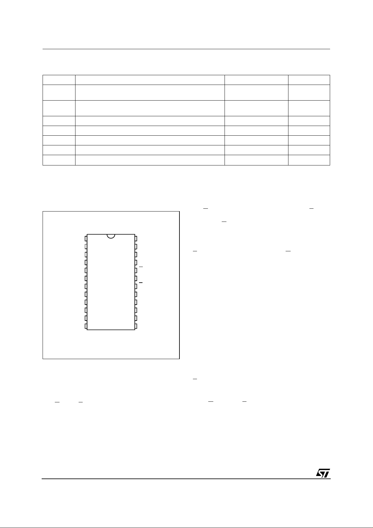
Figure 2. DIP Pin Connecti on s
A7
1
2
A6
3
A5
A4
4
5
A3
6
A2
A1
A0
Q0
Q1
Q2
V
SS
M2716
7
8
9
10
11
12
24
23
22
21
20
19
18
17
16
15
14
13
AI00785
V
CC
A8
A9
V
PP
G
A10
EP
Q7
Q6
Q5
Q4
Q3
DEVICE OPERATION
The M2716 has 3 m odes of operation in the normal
system environment . These are show n in Table 3.
Read Mode. The M2716 read operation requires
G = VIL, EP = VIL and that addresses A0-A10
that
have been stabilized. Valid data will appear on the
output pins after time t
AVQV
, t
GLQV
or t
ELQV
(see
Switching T ime Wavefor ms) depending on which is
limiting.
Deselect Mode. The M2716 is deselect ed by making
G = VIH. This mode is independent of EP and
the condition of the addresses. The outputs are
Hi-Z when
G = VIH. This allows tied-OR of 2 or more
M2716’s for memory expansion.
Standby Mo de (Power Down). The M2716 may
be powered down to the standby mode by making
EP = VIH. This is indep endent of G and automatically puts the o utputs in the Hi- Z st ate. The power
is reduced to 25% (132 mW max) of the normal
operating power . V
at 5V . Acces s time at power up remains either t
or t
(see Switching Tim e Waveforms).
ELQV
and VPP must be maintained
CC
A VQV
Programming
The M2716 is shipped from SGS-THOMS ON completely erased. All bits will be at “1" level (output
high) in this initial state and after any full erasure.
Table 3 shows the 3 programming modes.
Program Mode. The M2716 is programmed by
introducing “0"s into the desired locations. This is
done 8 bit s (a byte) at a t ime. Any indiv idual address ,
sequent i a l a ddresses, or add re sses chosen at r a ndom may be program med. Any or all of the 8 bits
associated with an addres s location may be programmed w ith a single program pulse applied to the
EP pin. A ll input volt age levels including the p rogram
pulse on chip enable are TTL compatible.
The programming sequence is: with V
= 25V , V
PP
CC
= 5V , G = VIH and EP = VIL, an address is select ed
and the desired data word is applied to the output
pins (V
= “0" and VIH = ”1" for both address and
IL
data). After the address and data signals are st able
the program pin is pulsed from V
to VIH with a
IL
2/9
Page 3
M2716
DEVICE OPERATION (cont’d)
pulse width between 45ms and 55ms. Multiple
pulses are not needed but will not cause device
damage. No pins should be left open. A high level
or higher) must not be maintained longer than
(V
IH
(max) on the program pin during p rogram-
t
PHPL
ming. M2716’s may be programmed in parallel in
this mode.
Program Verify Mode. The programming of the
M2716 may be verified either one byte at a time
during the programming (as shown in Figure 6) or
by reading all of the bytes out at the end of the
programming sequence. This can be done with
= 25V or 5V in either case. VPP must be at 5 V
V
PP
for all operating modes and can be maintained at
25V for all programming modes.
Program Inhibit Mod e. The program inhibit mode
allows several M2716’s to be programmed simultaneously with different data for each one by controlling which ones receive the program pulse. All
similar inputs of the M2716 may be paralleled.
Pulsing the prog ram pin (from V
to VIH) will pro-
IL
gram a unit while inhibiting the program pulse to a
unit will keep it from being programmed and k eep-
G = VIH will put its outputs in the Hi-Z state.
ing
ERASURE OPE RATION
The M2716 is erased by exposure to high int ensity
ultraviolet light through the transparent window.
This exposure discha rges the floating gate to its
initial state through induced photo current. It is
recommended that t he M2716 be kept out of direct
sunlight. The UV content of sunlight may cause
a partial erasure of some bit s in a relatively short
period of time.
An ultraviolet source of 2537 Å yielding a total
integrated dosage of 15 watt-seconds/cm
2
power
rating is used. The M2716 to be erased should be
placed 1 inch away from the lamp and no filters
should be used.
An erasure system should be calibrated periodically. The erasure time is increased by the
square of the distance (if the distance is doubled
the erasure time goes up by a factor of 4). Lamps
lose intensity as they age, it is theref ore important
to periodically check that the UV s ys tem is in good
order.
This will ensure that the EPROMs are being completely erased. Incomplete erasure will cause
symptoms that can be misleading. Programmers,
components, and system designs have been erroneously suspected when incomplete erasure was
the basic problem.
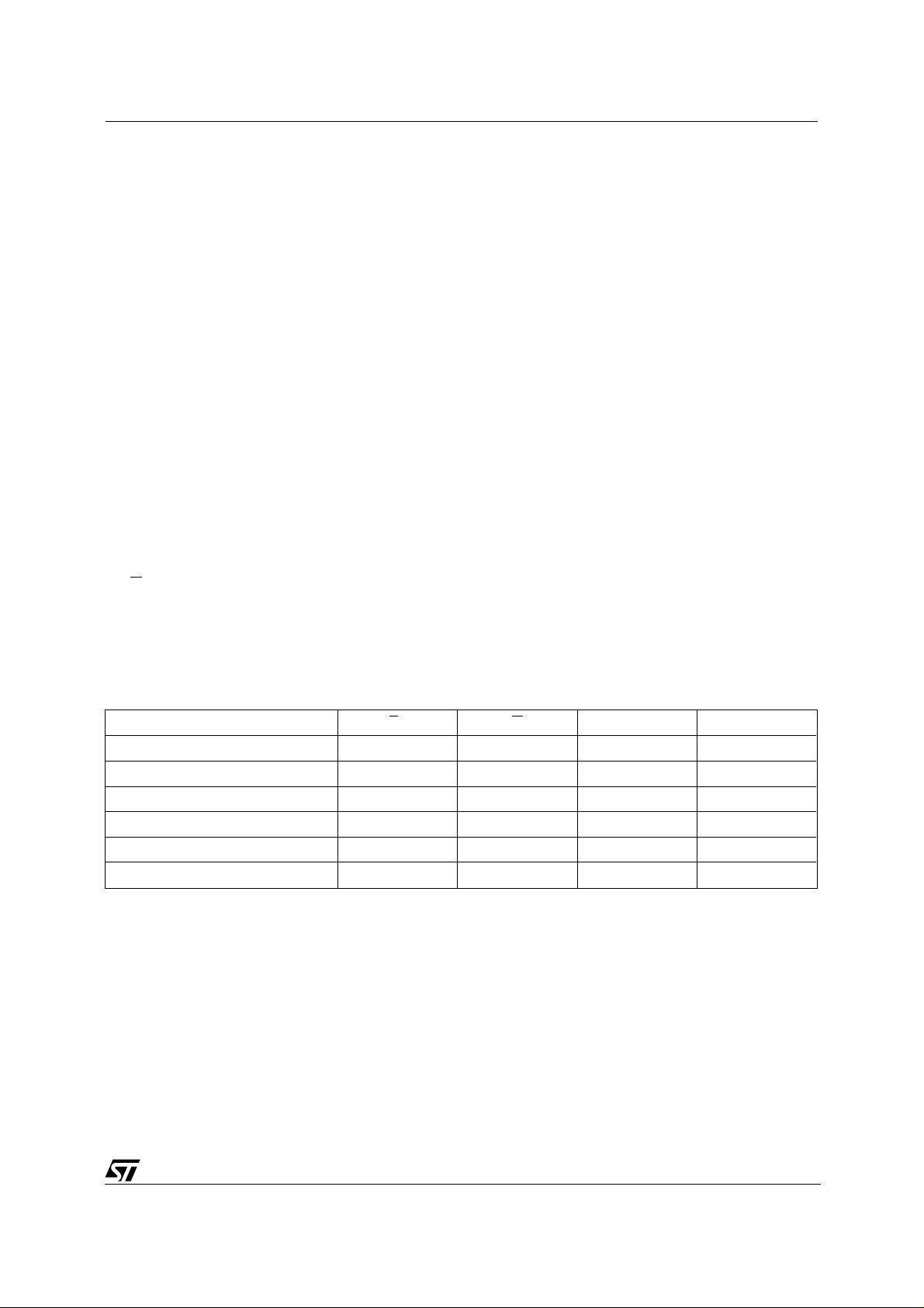
Table 3. Operating Modes
Mode EP GVPPQ0 - Q7
Read V
Program V
Verify V
Program Inhibit V
Deselect X V
Standby V
Note: X = VIH or VIL.
IL
Pulse V
IH
IL
IL
IH
V
IL
IH
V
IL
V
IH
IH
XVCCHi-Z
V
CC
V
PP
VPP or V
V
PP
V
CC
CC
Data Out
Data In
Data Out
Hi-Z
Hi-Z
3/9
Page 4
M2716
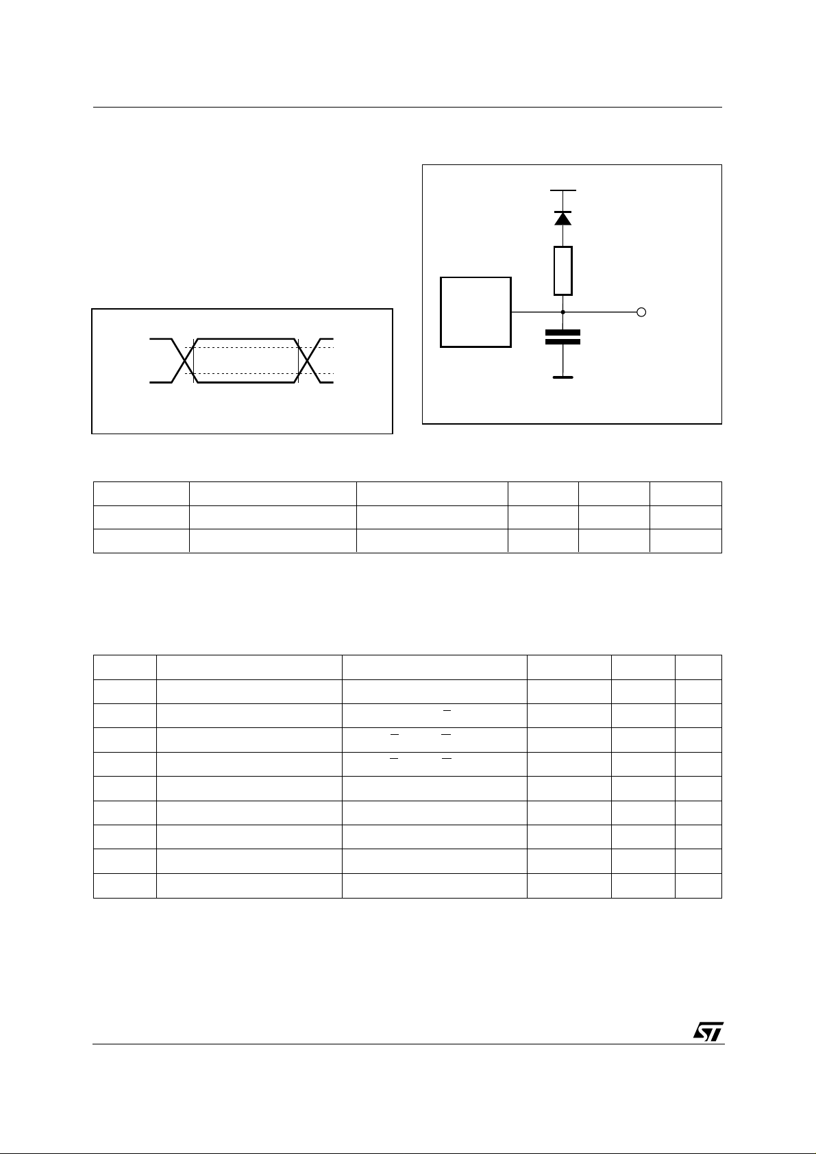
AC MEASUREMENT CONDITIONS
Input Rise and Fall Times ≤ 20ns
Figure 4. AC Testing Load Circuit
1.3V
Input Pulse Voltages 0.45V to 2.4V
Input and Output Timing Ref. Voltages 0.8V to 2.0V
1N914
Note that Output Hi-Z is defined as the point where data
is no longer driven.
3.3kΩ
Figure 3. AC T est ing Input Outpu t W avefo r m s
2.4V
0.45V
T able 4. Capacitance
(1)
(TA = 25 °C, f = 1 MHz )
2.0V
0.8V
AI00827
DEVICE
UNDER
TEST
CL = 100pF
CL includes JIG capacitance
Symbol Parameter Test Condition Min Max Unit
C
IN
C
OUT
Note: 1. Sampled only, not 100% tested.
Input Capacitance VIN = 0V 6 pF
Output Capacitance V
= 0V 12 pF
OUT
OUT
AI00828
T ab le 5. Read Mode DC Characteristi cs
(1)
(TA = 0 to 70 °C or –40 to 85 °C; VCC = 5V ± 5% or 5V ± 10%; VPP = VCC)
Symbol Parameter Test Condition Min Max Unit
I
I
LO
I
CC
I
CC1
I
PP
V
V
V
V
Note: 1. VCC must be applied simult aneously with or before VPP and removed simultaneously or after VPP.
Input Leakage Current 0 ≤ VIN ≤ V
LI
Output Leakage Current V
= VCC, EP = V
OUT
Supply Current EP = VIL, G = V
Supply Current (Standby) EP = VIH, G = V
Program Current VPP = V
Input Low Voltage –0.1 0.8 V
IL
Input High Voltage 2 VCC + 1 V
IH
Output Low Voltage IOL = 2.1mA 0.45 V
OL
Output High Voltage IOH = –400µA 2.4 V
OH
CC
CC
IL
IL
CC
±10 µA
±10 µA
100 mA
25 mA
5mA
4/9
Page 5
M2716
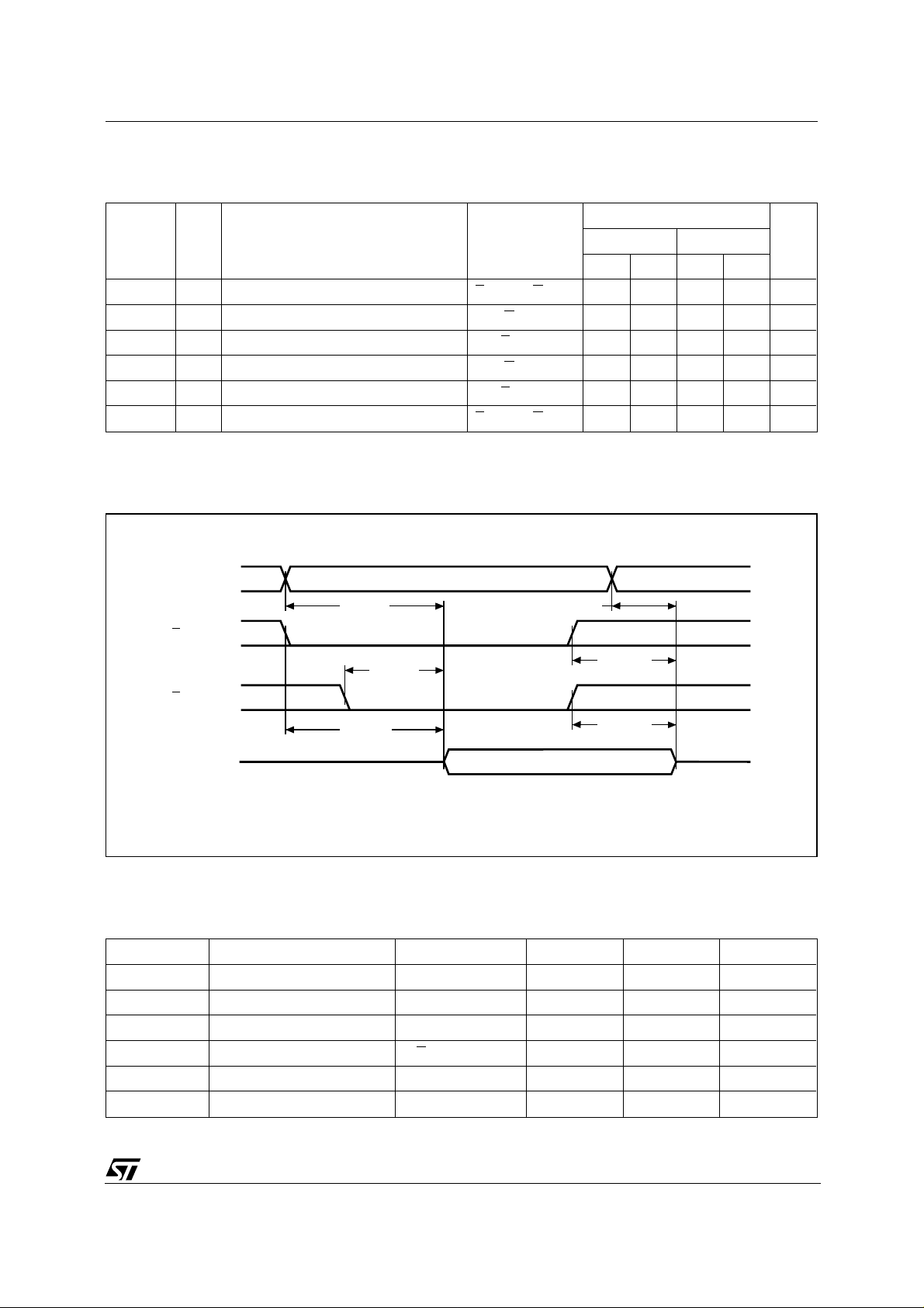
T ab le 6. Read Mod e AC Charact eristi cs
(1)
(TA = 0 to 70 °C or –40 to 85 °C; VCC = 5V ± 5% or 5V ± 10%; VPP = VCC)
Symbol Alt Parameter Test Condition
t
AVQV
t
ELQV
t
GLQV
t
EHQZ
t
GHQZ
t
AXQX
Notes: 1. VCC must be applied simult aneously with or before VPP and removed simultaneously or after VPP.
t
Address Valid to Output Valid EP = VIL, G = V
ACC
t
Chip Enable Low to Output Valid G = V
CE
t
Output Enable Low to Output Valid EP = V
OE
(2)
t
Chip Enable High to Output Hi-Z G = V
OD
(2)
t
Output Enable High to Output Hi-Z EP = V
DF
t
Address Transition to Output Transition EP = VIL, G = V
OH
2. Sampled only, not 100% test ed.
IL
IL
IL
IL
IL
IL
-1 blank
Min Max Min Max
0 100 0 100 ns
0 100 0 100 ns
00ns
Figure 5. Read Mode AC W avefo r ms
A0-A10
tAVQV
VALID
tAXQX
M2716
Unit
350 450 ns
350 450 ns
120 120 ns
EP
tGLQV
G
tELQV
Q0-Q7
T ab le 7. Program ming Mode DC Char acterist ics
DATA OUT
(1)
tEHQZ
tGHQZ
(TA = 25 °C; VCC = 5V ± 5%; VPP = 25V ± 1V)
Symbol Parameter Test Condition Min Max Unit
I
LI
I
CC
I
PP
I
PP1
V
IL
V
IH
Note: 1. VCC must be applied simult aneously with or before VPP and removed simultaneously or after VPP.
Input Leakage Current VIL ≤ VIN ≤ V
IH
Supply Current 100 mA
Program Current 5 mA
Program Current Pulse EP = VIH Pulse 30 mA
Input Low Voltage –0.1 0.8 V
Input High Voltage 2 VCC + 1 V
±10 µA
Hi-Z
AI00786
5/9
Page 6
M2716
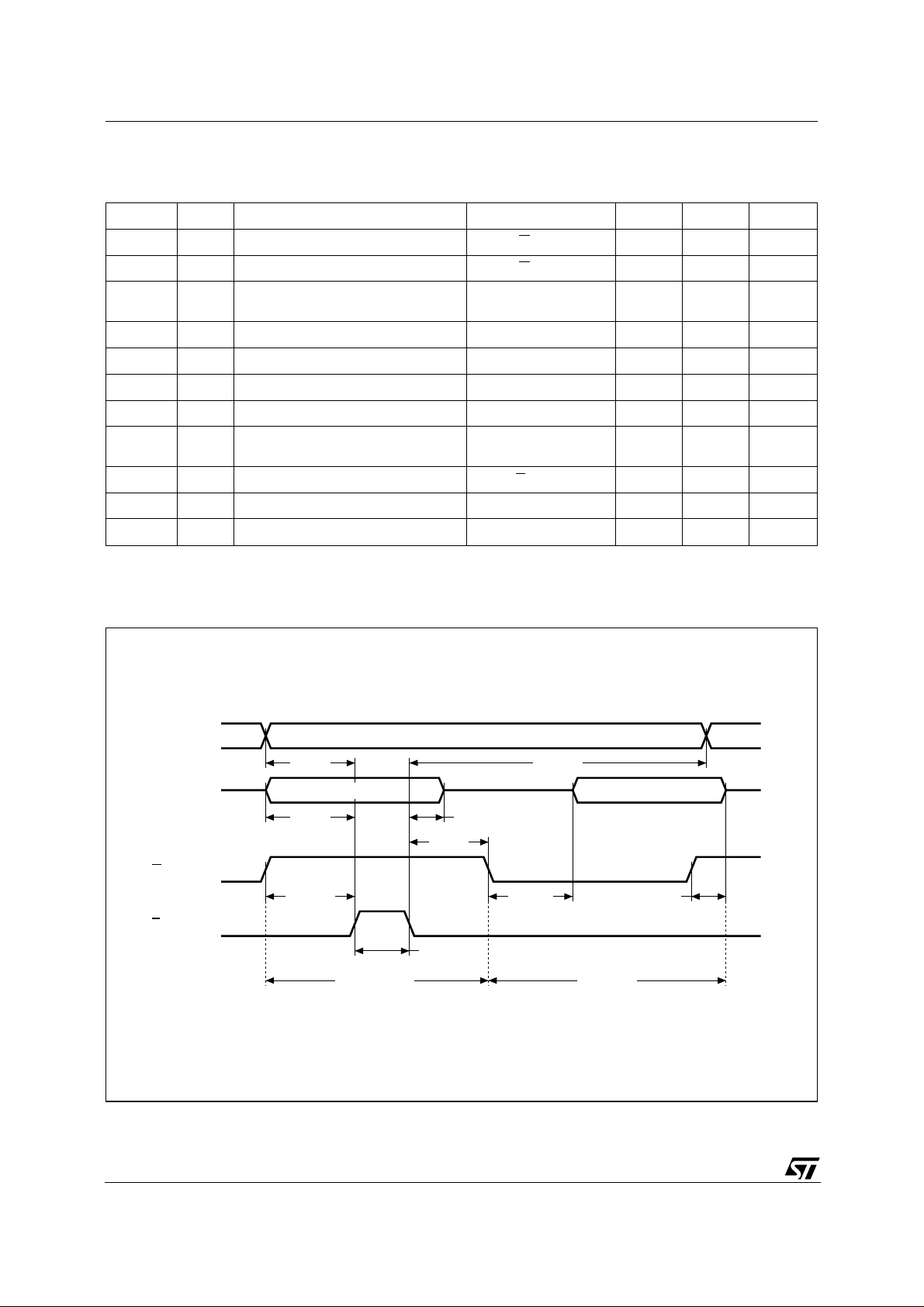
Tab l e 8. Programmi ng M ode AC Ch aracteri stics
(1)
(TA = 25 °C; VCC = 5V ± 5%; VPP = 25V ± 1V)
Symbol Alt Parameter Test Condition Min Max Units
t
AVPH
t
QVPH
t
GHPH
t
PL1PL2
t
PH1PH2
t
PHPL
t
PLQX
t
PLGX
t
GLQV
t
GHQZ
t
PLAX
Notes: 1. VCC must be applied simultaneously with or before VPP and removed simultaneously or after VPP.
2. Sampled only, not 100% tested.
t
t
t
t
t
t
t
t
t
t
t
Address Valid to Program High G = V
AS
Input Valid to Program High G = V
DS
Output Enable High to Program
OS
IH
IH
High
Program Pulse Rise Time 5 ns
PR
Program Pulse Fall Time 5 ns
PF
Program Pulse Width 45 55 ms
PW
Program Low to Input Transition 2 µs
DH
Program Low to Output Enable
OH
Transition
Output Enable to Output Valid EP = V
OE
Output Enable High to Output Hi-Z 0 100 ns
DF
Program Low to Address Transition 2 µs
AH
IL
2 µs
2 µs
2 µs
2 µs
120 ns
Figure 6. Programmi ng and Verify Modes AC Wavefor m s
6/9
A0-A10
Q0-Q7
G
EP
tAVPH
tQVPH
tGHPH
DATA IN
PROGRAM
tPLGX
tPHPL
tPLQX
VALID
tGLQV
tPLAX
DATA OUT
tGHQZ
VERIFY
AI00787
Page 7

Ordering Inform at ion S chem e
Example: M2716 -1 F 1
Device Type
M2716 = NMOS 16 Kbit (2Kb x 8) UV EPROM
M2716
Speed and V
= 350 ns, 5V ± 10%
-1
blank = 450 ns, 5V ± 5%
Package
F = FDIP24W
Temperature Range
1 = –0 to 70 °C
6 = –40 to 85 °C
Tolerance
CC
For a list of available options (Speed, Pac kage, etc...) or for furthe r information on any aspect of this device, please contact the ST Sales Office nearest to you.
7/9
Page 8
M2716
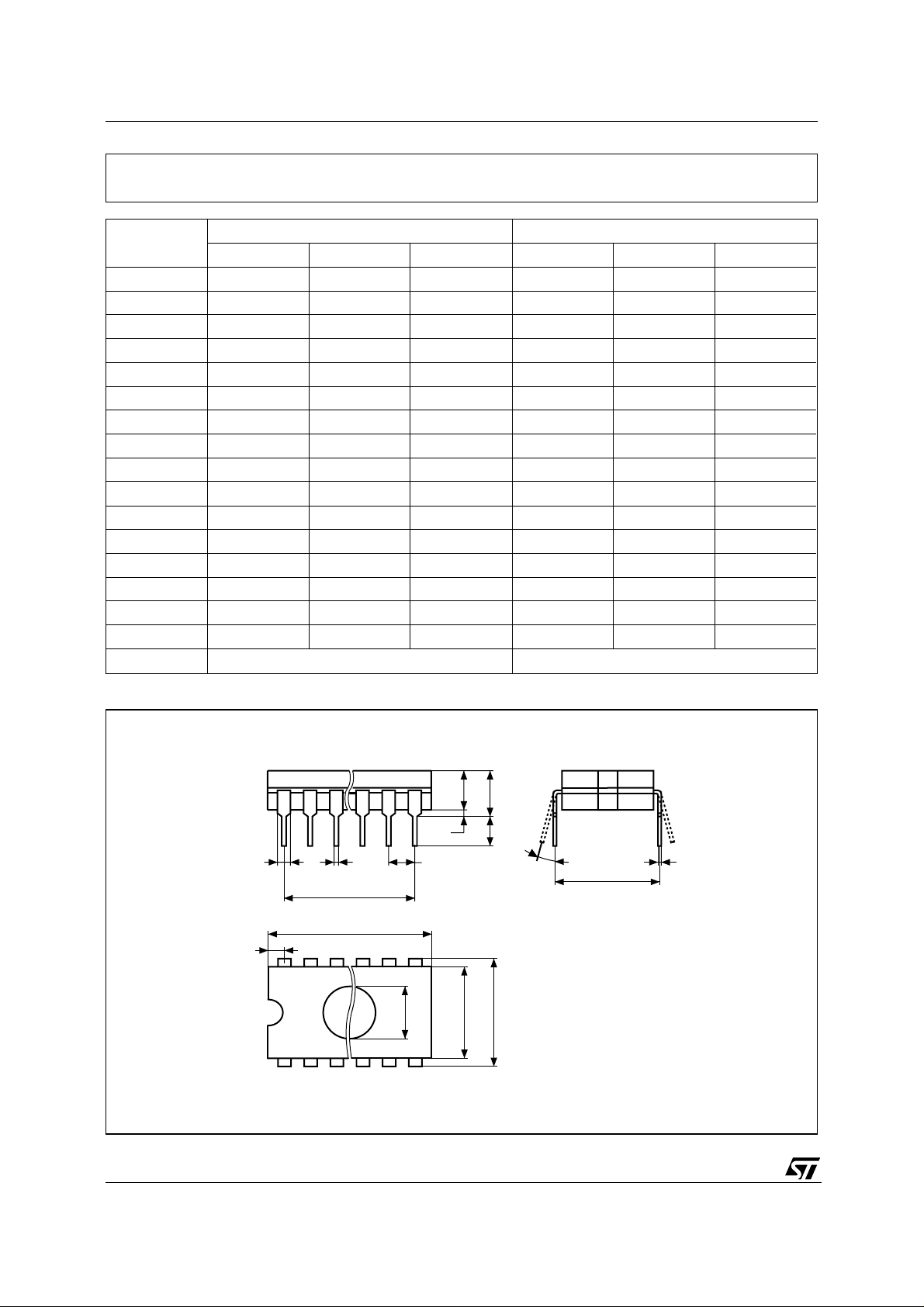
FDIP24W - 24 pin Ceramic Frit-seal DIP, with window
Symb
Typ Min Max Typ Min Max
A 5.71 0.225
A1 0.50 1.78 0.020 0.070
A2 3.90 5.08 0.154 0.200
B 0.40 0.55 0.016 0.022
B1 1.17 1.42 0.046 0.056
C 0.22 0.31 0.009 0.012
D 32.30 1.272
E 15.40 15.80 0.606 0.622
E1 13.05 13.36 0.514 0.526
e1 2.54 – – 0.100 – –
e3 27.94 – – 1.100 – –
eA 16.17 18.32 0.637 0.721
L 3.18 4.10 0.125 0.161
S 1.52 2.49 0.060 0.098
∅ 7.11 – – 0.280 – –
α 4° 15° 4° 15°
N24 24
mm inches
Drawing is not to scale
8/9
B1 B e1
e3
D
S
N
∅
1
A2
A1AL
Cα
eA
E1 E
FDIPW-a
Page 9

M2716
Information furnished is believed to be accurate and reliable. However, STMicroelectronics assumes no responsibility for the consequences
of use of such information nor for any infringement of patents or other rights of third parties which may result from its use. No license is granted
by implic ation or otherwise under any patent or patent rights of STMi croelectr onics. Specifications mentioned in thi s publicati on are subject
to change without notice. This publication supersedes and replaces all information previously supplied. STMicroelectronics products are not
authorized for use as cri tical comp onents in life support dev i ces or systems wi t hout express written ap proval of STMi croelect ro nics.
The ST log o i s registered trademark of STMicroelectronics
2000 ST M icroelec tronics - All Ri ghts Rese rved
All other na m es are the prop erty of their respectiv e owners.
Australi a - B razil - China - Finland - F rance - Germ any - Hong Kon g - India - Italy - Japan - Mala ysia - Malta - Morocco -
Singapor e - Spain - Swede n - S wi tzerland - United Kingdom - U.S.A .
STMicroelectronics GROUP OF COMPANIES
http://www.st.com
9/9
 Loading...