

Page 1
FM24C02U/03U – 2K-Bit Standard 2-Wire Bus
Interface Serial EEPROM
FM24C02U/03U – 2K-Bit Standard 2-Wire Bus Interface Serial EEPROM
August 2000
General Description
The FM24C02U/03U devices are 2048 bits of CMOS non-volatile
electrically erasable memory. These devices conform to all specifications in the Standard IIC 2-wire protocol. They are designed to
minimize device pin count and simplify PC board layout requirements.
The upper half (upper 1Kbit) of the memory of the FM24C03U can
be write protected by connecting the WP pin to VCC. This section of
memory then becomes unalterable unless WP is switched to VSS.
This communications protocol uses CLOCK (SCL) and DATA
I/O (SDA) lines to synchronously clock data between the master
(for example a microprocessor) and the slave EEPROM device(s).
The Standard IIC protocol allows for a maximum of 16K of
EEPROM memory which is supported by the Fairchild family in
2K, 4K, 8K, and 16K devices, allowing the user to configure the
memory as the application requires with any combination of
EEPROMs. In order to implement higher EEPROM memory
densities on the IIC bus, the Extended IIC protocol must be used.
(Refer to the FM24C32 or FM24C65 datasheets for more information.)
Fairchild EEPROMs are designed and tested for applications requiring high endurance, high reliability and low power consumption.
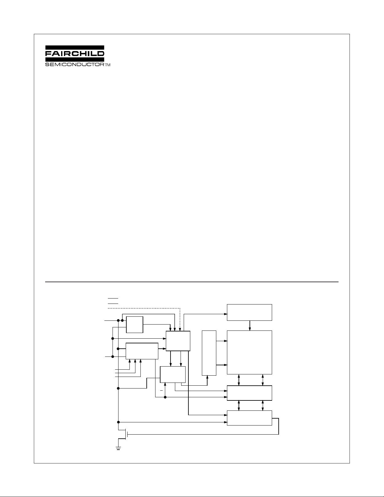
Block Diagram
V
CC
V
SS
WP
SDA
SCL
START
STOP
LOGIC
SLAVE ADDRESS
REGISTER &
COMPARATOR
CONTROL
LOGIC
Features
■ Extended operating voltage 2.7V – 5.5V
■ 400 KHz clock frequency (F) at 2.7V - 5.5V
■ 200µA active current typical
10µA standby current typical
1µA standby current typical (L)
0.1µA standby current typical (LZ)
■ IIC compatible interface
– Provides bi-directional data transfer protocol
■ Sixteen byte page write mode
– Minimizes total write time per byte
■ Self timed write cycle
Typical write cycle time of 6ms
■ Hardware Write Protect for upper half (FM24C03U only)
■ Endurance: 1,000,000 data changes
■ Data retention greater than 40 years
■ Packages available: 8-pin DIP, 8-pin SO, and 8-pin TSSOP
■ Available in three temperature ranges
- Commercial: 0° to +70°C
- Extended (E): -40° to +85C
- Automotive (V): -40° to +125°C
H.V. GENERATION
TIMING &CONTROL
XDEC
E2PROM
ARRAY
A2
A1
A0
© 2000 Fairchild Semiconductor International
FM24C02U/03U Rev. A.3
R/W
WORD
ADDRESS
COUNTER
D
IN
YDEC
CK
DATA REGISTER
1
D
OUT
www.fairchildsemi.com
Page 2
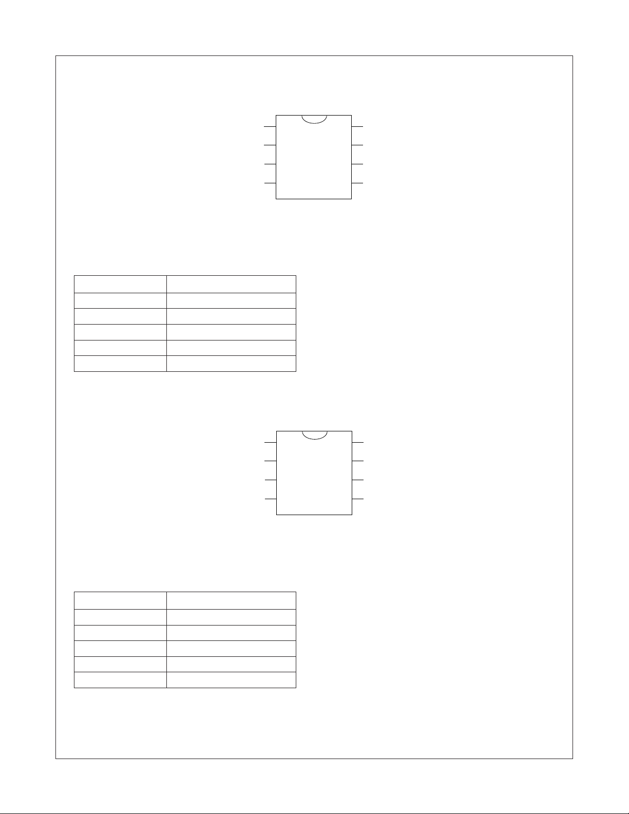
Connection Diagrams
Dual-in-Line Package (N), SO Package (M8) and TSSOP Package (MT8)
FM24C02U/03U – 2K-Bit Standard 2-Wire Bus Interface Serial EEPROM
Pin Names
A0,A1,A2 Device Address Inputs
V
SS
SDA Serial Data I/O
SCL Serial Clock Input
NC No Connection
V
CC
Dual-in-Line Package (N), SO Package (M8) and TSSOP Package (MT8)
Ground
Power Supply
A0
1
A1
2
A2
V
SS
24C02
3
4
V
8
CC
NC
7
SCL
6
SDA
5
See Package Number N08E, M08A and MTC08
Pin Names
A0,A1,A2 Device Address Inputs
V
SS
SDA Serial Data I/O
SCL Serial Clock input
WP Write Protect
V
CC
Ground
Power Supply
A0
1
A1
2
A2
V
SS
24C03
3
4
V
8
CC
WP
7
SCL
6
SDA
5
See Package Number N08E, M08A and MTC08
FM24C02U/03U Rev. A.3
2
www.fairchildsemi.com
Page 3
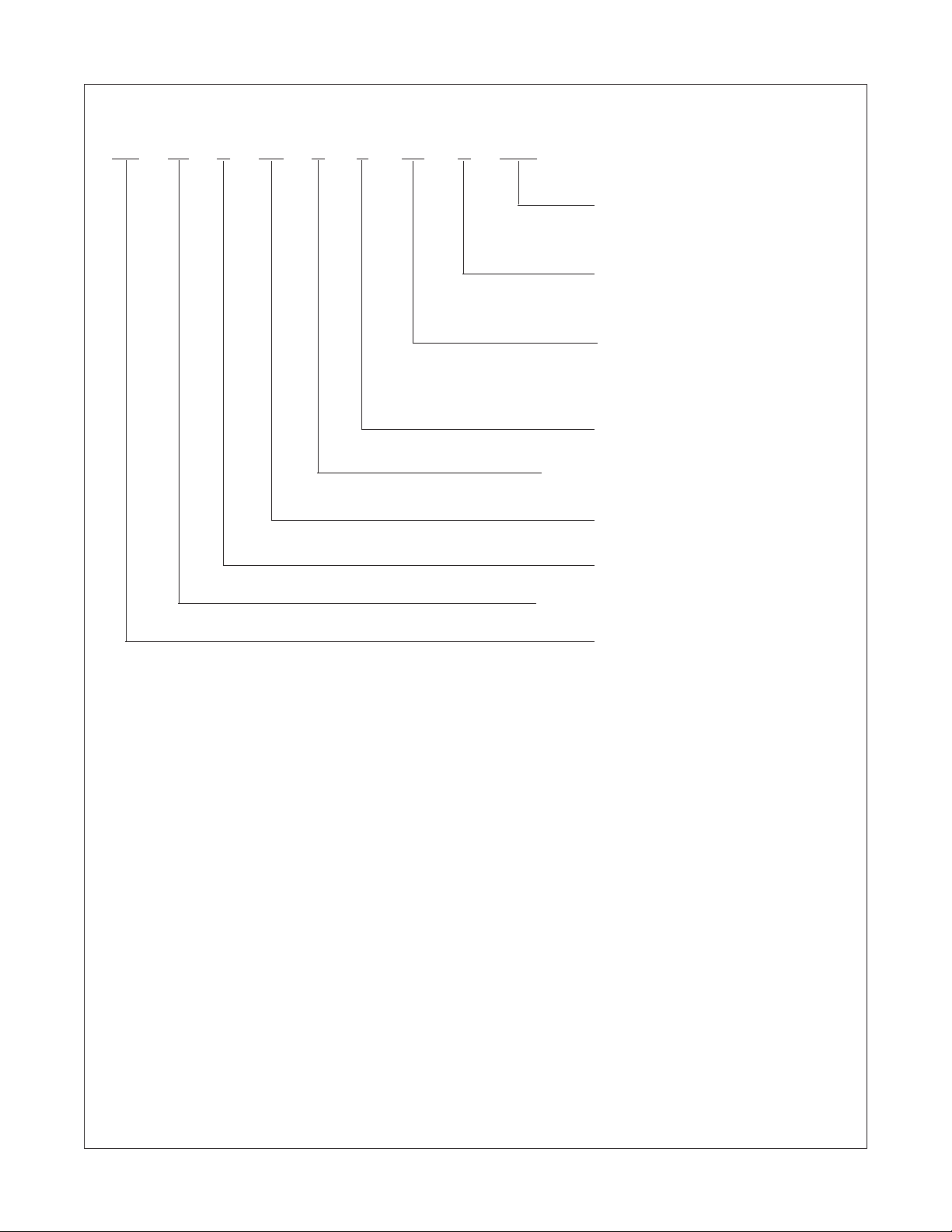
Ordering Information
FM 24 C XX U F LZ E XXX Letter Description
FM24C02U/03U – 2K-Bit Standard 2-Wire Bus Interface Serial EEPROM
Package N 8-pin DIP
Temp. Range Blank 0 to 70°C
Voltage Operating Range Blank 4.5V to 5.5V
SCL Clock Frequency Blank 100KHz
Process U Ultralite CS100UL
Density 02 2K
Interface 24 IIC
M8 8-pin SOIC
MT8 8-pin TSSOP
V -40 to +125°C
E -40 to +85°C
L 2.7V to 5.5V
LZ 2.7V to 5.5V and
<1µA Standby Current
F 400KHz
03 2K with Write Protect
C CMOS Technology
FM Fairchild Non-Volatile
Memory
FM24C02U/03U Rev. A.3
3
www.fairchildsemi.com
Page 4
Product Specifications
FM24C02U/03U – 2K-Bit Standard 2-Wire Bus Interface Serial EEPROM
Absolute Maximum Ratings
Ambient Storage Temperature –65°C to +150°C
All Input or Output Voltages
with Respect to Ground –0.3V to 6.5V
Lead Temperature
(Soldering, 10 seconds) +300°C
ESD Rating 2000V min.
Operating Conditions
Ambient Operating Temperature
FM24C02U/03U 0°C to +70°C
FM24C02UE/03UE -40°C to +85°C
FM24C02UV/03UV -40°C to +125°C
Positive Power Supply
FM24C02U/03U 4.5V to 5.5V
FM24C02UL/03UL 2.7V to 5.5V
FM24C02ULZ/03ULZ 2.7V to 5.5V
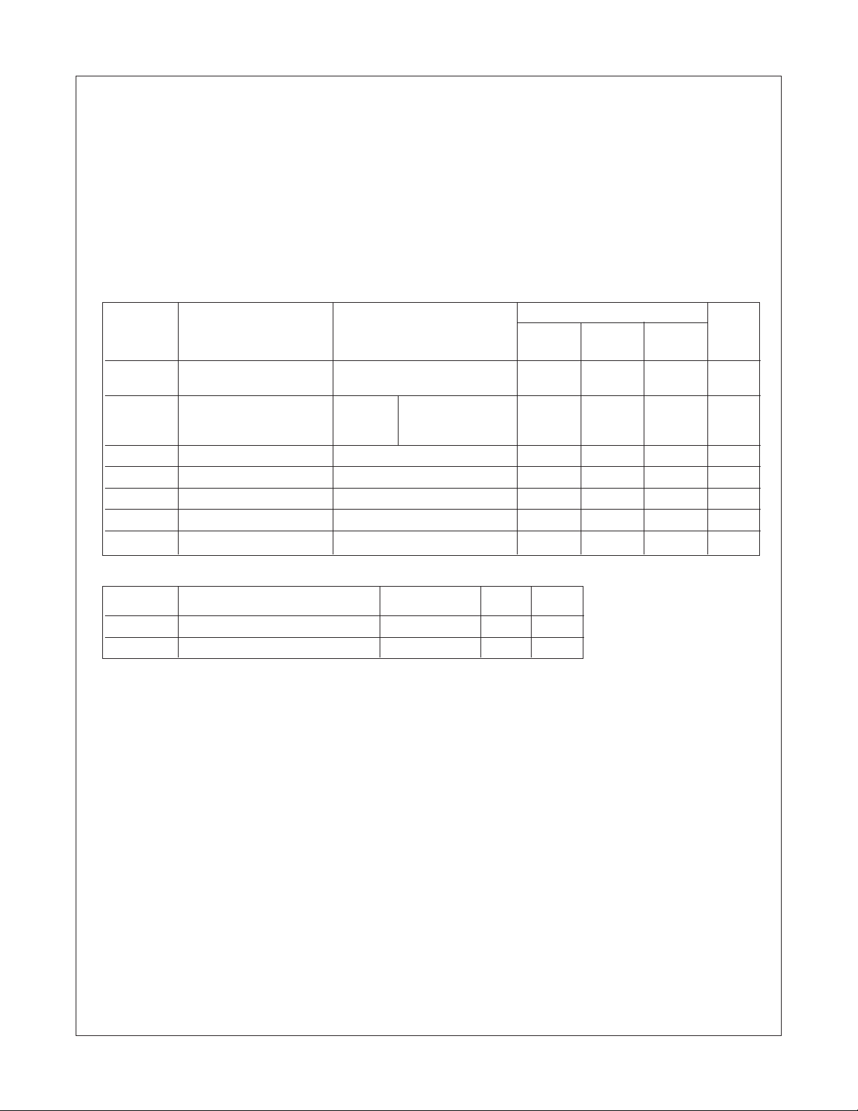
DC Electrical Characteristics (2.7V to 5.5V)
Symbol Parameter Test Conditions Limits Units
Min Typ Max
(Note 1)
I
CCA
I
SB
(Note 3) or V
I
LI
I
LO
V
IL
V
IH
V
OL
Active Power Supply Current f
= 400 KHz ("F" Version) 0.2 1.0 mA
SCL
f
= 100 KHz
SCL
Standby Current VIN = GND VCC = 2.7V - 5.5V 10 50 µA
CC
VCC = 2.7V - 5.5V (L) 1 10 µA
VCC = 2.7V - 4.5V (LZ) 0.1 1 µA
Input Leakage Current VIN = GND to V
Output Leakage Current V
= GND to V
OUT
CC
CC
Input Low Voltage –0.3 V
0.1 1 µA
0.1 1 µA
x 0.3 V
CC
Input High Voltage VCC x 0.7 VCC + 0.5 V
Output Low Voltage IOL = 3 mA 0.4 V
Capacitance T
= +25°C, f = 100/400 KHz, VCC = 5V (Note 2)
A
Symbol Test Conditions Max Units
C
I/O
C
IN
Note 1: Typical values are TA = 25°C and nominal supply voltage of 5V for 4.5V-5.5V operation and at 3V for 2.7V-4.5V operation.
Note 2: This parameter is periodically sampled and not 100% tested.
Note 3: The "L" and "LZ" versions can be operated in the 2.7V to 5.5V VCC range. However, for a standby current (ISB) of 1µA, the VCC should be within 2.7V to 4.5V.
Input/Output Capacitance (SDA) V
= 0V 8 pF
I/O
Input Capacitance (A0, A1, A2, SCL) VIN = 0V 6 pF
FM24C02U/03U Rev. A.3
4
www.fairchildsemi.com
Page 5
FM24C02U/03U – 2K-Bit Standard 2-Wire Bus Interface Serial EEPROM
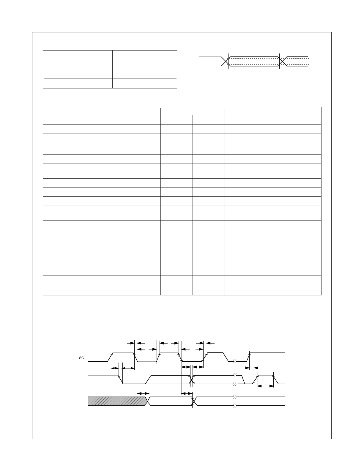
AC Test Conditions
Input Pulse Levels VCC x 0.1 to VCC x 0.9
Input Rise and Fall Times 10 ns
AC Testing Input/Output Waveforms
0.9VCC
0.1VCC
Input & Output Timing Levels VCC x 0.3 to VCC x 0.7
Output Load 1 TTL Gate and C
= 100 pF
L
Read and Write Cycle Limits (Standard and Low VCC Range 2.7V - 5.5V)
Symbol Parameter 100 KHz 400 KHz Units
Min Max Min Max
f
SCL
T
I
t
AA
t
BUF
t
HD:STA
t
LOW
t
HIGH
t
SU:STA
t
HD:DAT
t
SU:DAT
t
R
t
F
t
SU:STO
t
DH
t
WR
(Note 4) 4.5V to 5.5V V
SCL Clock Frequency 100 400 KHz
Noise Suppression Time Constant at
SCL, SDA Inputs (Minimum V
IN
100 50 ns
Pulse width)
SCL Low to SDA Data Out Valid 0.3 3.5 0.1 0.9 µs
Time the Bus Must Be Free before 4.7 1.3 µs
a New Transmission Can Start
Start Condition Hold Time 4.0 0.6 µs
Clock Low Period 4.7 1.5 µs
Clock High Period 4.0 0.6 µs
Start Condition Setup Time 4.7 0.6 µs
(for a Repeated Start Condition)
Data in Hold Time 0 0 ns
Data in Setup Time 250 100 ns
SDA and SCL Rise Time 1 0.3 µs
SDA and SCL Fall Time 300 300 ns
Stop Condition Setup Time 4.7 0.6 µs
Data Out Hold Time 300 50 ns
Write Cycle Time
10 10 ms
15 15
2.7V to 4.5V V
CC
CC
0.7VCC
0.3VCC
Note 4: The write cycle time (tWR) is the time from a valid stop condition of a write sequence to the end of the internal erase/program cycle. During the write cycle, the
FM24C02U/03U bus interface circuits are disabled, SDA is allowed to remain high per the bus-level pull-up resistor, and the device does not respond to its slave address. Refer
"Write Cycle Timing" diagram.
Bus Timing
t
LOW
t
R
t
t
SU:DAT
t
DH
SU:STO
t
BUF
www.fairchildsemi.com
FM24C02U/03U Rev. A.3
SCL
SDA
SDA
OUT
t
F
t
t
LOW
t
SU:STA
IN
t
HD:STA
HIGH
t
HD:DAT
t
AA
5
Page 6
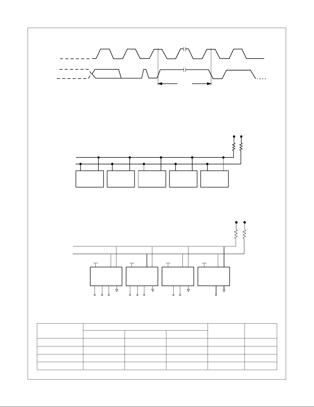
Write Cycle Timing
SCL
FM24C02U/03U – 2K-Bit Standard 2-Wire Bus Interface Serial EEPROM
SDA
Note: The write cycle time (tWR) is the time from a valid stop condition of a write sequence to the end of the internal erase/program cycle.
8th BIT ACK
WORD n
STOP
CONDITION
t
WR
START
CONDITION
Typical System Configuration
SDA
SCL
Master
Transmitter/
Receiver
Note: Due to open drain configuration of SDA and SCL, a bus-level pull-up resistor is called for, (typical value = 4.7kΩ)
Slave
Receiver
Slave
Transmitter/
Receiver
Master
Transmitter
Master
Transmitter/
Receiver
Example of 16K of Memory on 2-Wire Bus
Note: The SDA pull-up resistor is required due to the open-drain/open collector output of IIC bus devices.
The SCL pull-up resistor is recommended because of the normal SCL line inactive 'high' state.
It is recommended that the total line capacitance be less than 400pF
V
CC
V
CC
V
CC
V
CC
SDA
SCL
Device Address Pins Present Memory Size # of Page
FM24C02U/03U Yes Yes Yes 2048 Bits 1
FM24C04U/05U No Yes Yes 4096 Bits 2
FM24C08U/09U No No Yes 8192 Bits 4
FM24C16U/17U No No No 16,384 Bits 8
FM24C02U/03U Rev. A.3
V
CC
24C02/03
A0 A1 A2 V
To
To
SS
To
V
V
SS
SS
V
SS
V
CC
24C02/03
A0 A1 A2 V
To
To
CC
To
V
V
SS
SS
V
SS
V
CC
24C04/05
A1 A2 V
To
To
V
V
CC
SS
SS
V
CC
24C08/09
A2 V
To
V
CC
SS
A0 A1 A2 Blocks
6
www.fairchildsemi.com
Page 7
FM24C02U/03U – 2K-Bit Standard 2-Wire Bus Interface Serial EEPROM
Background Information (IIC Bus)
IIC bus allows synchronous bi-directional communication between a TRANSMITTER and a RECEIVER using a Clock signal
(SCL) and a Data signal (SDA). Additionally there are up to three
Address signals (A2, A1 and A0) which collectively serve as "chip
select signal" to a device (example EEPROM) on the IIC bus.
All communication on the IIC bus must be started with a valid
START condition (by a MASTER), followed by transmittal (by the
MASTER) of byte(s) of information (Address/Data). For every byte
of information received, the addressed RECEIVER provides a valid
ACKNOWLEDGE pulse to further continue the communication
unless the RECEIVER intends to discontinue the communication.
Depending on the direction of transfer (Write or Read), the RECEIVER can be a SLAVE or the MASTER. A typical IIC communication concludes with a STOP condition (by the MASTER).
Addressing an EEPROM memory location involves sending a
command string with the following information:
[DEVICE TYPE]—[DEVICE/PAGE BLOCK SELECTION]—[R/W
BIT]—{acknowledge pulse}—[ARRAY ADDRESS]
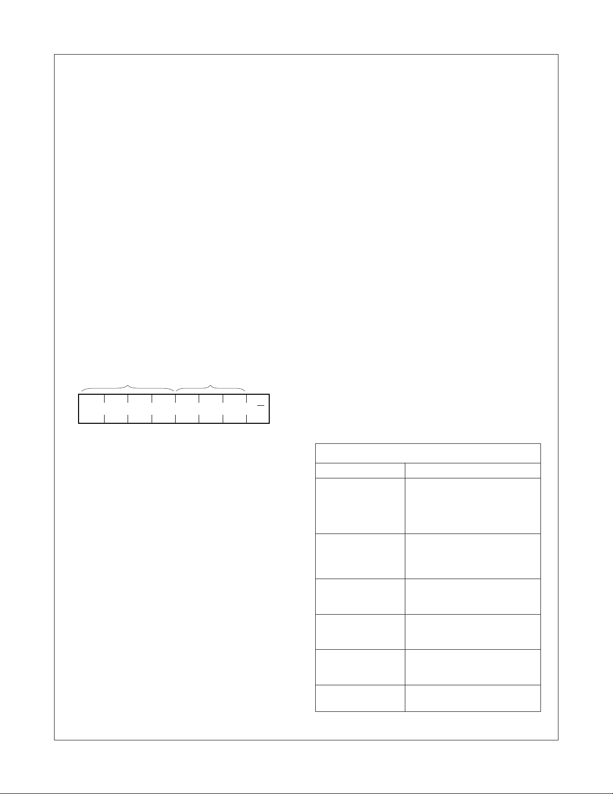
Slave Address
Slave Address is an 8-bit information consisting of a Device type
field (4bits), Device/Page block selection field (3bits) and Read/
Write bit (1bit).
Slave Address Format
Device Type
Identifier
1 0 1 0 A2 A1 A0 R/W (LSB)
Device/Page Block
Selection
Acknowledge
Acknowledge is an active LOW pulse on the SDA line driven by an
addressed receiver to the addressing transmitter to indicate
receipt of 8-bits of data. The receiver provides an ACK pulse for
every 8-bits of data received. This handshake mechanism is done
as follows: After transmitting 8-bits of data, the transmitter releases the SDA line and waits for the ACK pulse. The addressed
receiver, if present, drives the ACK pulse on the SDA line during
the 9th clock and releases the SDA line back (to the transmitter).
Refer
Figure 3
.
Array Address
Array address is an 8-bit information containing the address of a
memory location to be selected within a page block of the device.
16K bit Addressing Limitation:
Standard IIC specification limits the maximum size of EEPROM
memory on the bus to 16K bits. This limitation is due to the
addressing protocol implemented which consists of the 8-bit Slave
Address and an additional 8-bit field called Array Address. This
Array Address selects 1 out of 256 locations (28=256). Since the
data format of IIC specification is 8-bit wide, a total of 256 x 8 =
2048 = 2K bits now becomes addressable by this 8-bit Array
Address. These 2K bits are typically referred as a “Page Block”.
Combining this 8-bit Array Address with the 3-bit Device/Page
address (part of Slave Address) allows a maximum of 8 pages
(23=8) of memory that can be addressed. Since each page is 2K
bits in size, 8 x 2K bits = 16K bits is the maximum size of memory
that is addressable on the Standard IIC bus. This 16Kb of memory
can be in the form of a single 16Kb EEPROM device or multiple
EEPROMs of varying density (in 2Kb multiples) to a maximum
total of 16Kb. To address the needs of systems that require more
than 16Kb on the IIC bus, a different specification called “Ex-
tended IIC Specification” is used.
Device Type
IIC bus is designed to support a variety of devices such as RAMs,
EPROMs etc., along with EEPROMS. Hence to properly identify
various devices on the IIC bus, a 4-bit “Device Type” identifier
string is used. For EEPROMS, this 4-bit string is 1-0-1-0. Every IIC
device on the bus internally compares this 4-bit string to its own
“Device Type” string to ensure proper device selection.
Device/Page Block Selection
When multiple devices of the same type (e.g. multiple EEPROMS)
are present on the IIC bus, then the A2, A1 and A0 address
information bits are also used as part of the Slave Address. Every
IIC device on the bus internally compares this 3-bit string to its own
physical configuration (A2, A1 and A0 pins) to ensure proper
device selection. This comparison is in addition to the “Device
Type” comparison. In addition to selecting an EEPROM, these 3
bits are also used to select a “page block” within the selected
EEPROM. Each page block is 2Kbit (256Bytes) in size. Depending on the density, an EEPROM can contain from a minimum of 1
to a maximum of 8 page blocks (in multiples of 2) and selection of
a page block within a device is by using A2, A1 and A0 bits.
Read/Write Bit
Last bit of the Slave Address indicates if the intended access is
Read or Write. If the bit is "1," then the access is Read, whereas
if the bit is "0," then the access is Write.
DEFINITIONS
WORD 8 bits (byte) of data
PAGE 16 sequential byte locations
starting at a 16-byte address
boundary, that may be programmed during a "page write"
programming cycle
PAGE BLOCK 2048 (2K) bits organized into 16
pages of addressable memory. (8
bits) x (16 bytes) x (16 pages) =
2048 bits
MASTER Any IIC device CONTROLLING the
transfer of data (such as a
microprocessor)
SLAVE Device being controlled
(EEPROMs are always considered
Slaves)
TRANSMITTER Device currently SENDING data on
the bus (may be either a Master or
Slave).
RECEIVER Device currently RECEIVING data
on the bus (Master or Slave)
FM24C02U/03U Rev. A.3
7
www.fairchildsemi.com
Page 8
FM24C02U/03U – 2K-Bit Standard 2-Wire Bus Interface Serial EEPROM
Pin Descriptions
Serial Clock (SCL)
The SCL input is used to clock all data into and out of the device.
Serial Data (SDA)
SDA is a bi-directional pin used to transfer data into and out of the
device. It is an open drain output and may be wire–ORed with any
number of open drain or open collector outputs.
Write Protect (WP) (FM24C03U Only)
If tied to VCC, PROGRAM operations onto the upper half (upper
1Kbits) of the memory will not be executed. READ operations are
possible. If tied to V
WRITE over the entire memory is possible.
This feature allows the user to assign the upper half of the memory
as ROM which can be protected against accidental programming.
When write is disabled, slave address and word address will be
acknowledged but data will not be acknowledged.
This pin has an internal pull-down circuit. However, on systems
where write protection is not required it is recommended that this
pin is tied to V
SS
Device Selection Inputs A2, A1 and A0 (as
appropriate)
These inputs collectively serve as “chip select” signal to an
EEPROM when multiple EEPROMs are present on the same IIC
bus. Hence these inputs, if present, should be connected to V
or VSS in a unique manner to allow proper selection of an EEPROM
amongst multiple EEPROMs. During a typical addressing sequence, every EEPROM on the IIC bus compares the configuration of these inputs to the respective 3 bit “Device/Page block
selection” information (part of slave address) to determine a valid
selection. For e.g. if the 3 bit “Device/Page block selection” is 10-1, then the EEPROM whose “Device Selection inputs” (A2, A1
and A0) are connected to VCC-VSS-V
Depending on the density, only appropriate numbers of “Device
Selection inputs” are provided on an EEPROM. For every “Device
selection input” that is not present on the device, the corresponding bit in the “Device/Page block selection” field is used to select
a “Page Block” within the device instead of the device itself.
Following table illustrates the above:
, normal operation is enabled, READ/
SS
.
respectively, is selected.
CC
CC
Device Operation
The FM24C02U/03U supports a bi-directional bus oriented protocol. The protocol defines any device that sends data onto the bus
as a transmitter and the receiving device as the receiver. The
device controlling the transfer is the master and the device that is
controlled is the slave. The master will always initiate data
transfers and provide the clock for both transmit and receive
operations. Therefore, the FM24C02U/03U will be considered a
slave in all applications.
Clock and Data Conventions
Data states on the SDA line can change only during SCL LOW.
SDA state changes during SCL HIGH are reserved for indicating
start and stop conditions. Refer to
page.
Start Condition
All commands are preceded by the start condition, which is a
HIGH to LOW transition of SDA when SCL is HIGH. The
FM24C02U/03U continuously monitors the SDA and SCL lines for
the start condition and will not respond to any command until this
condition has been met.
Stop Condition
All communications are terminated by a stop condition, which is a
LOW to HIGH transition of SDA when SCL is HIGH. The stop
condition is also used by the FM24C02U/03U to place the device
in the standby power mode, except when a Write operation is
being executed, in which case a second stop condition is required
after tWR period, to place the device in standby mode.
Figure 1
and
Figure 2
on next
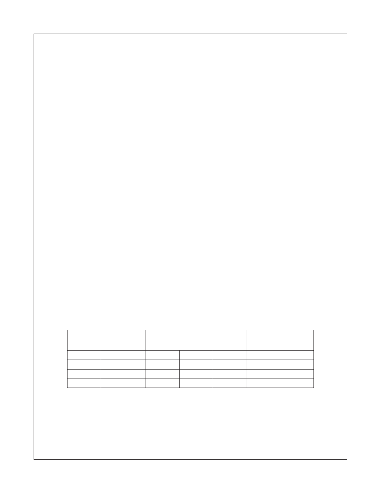
EEPROM Number of Device Selection Inputs Address Bits
Density Page Blocks Provided Selecting Page Block
2k bit 1 A0 A1 A2 None
4k bit 2 — A1 A2 A0
8k bit 4 ——A2 A0 and A1
16k bit 8 ——— A0, A1 and A2
Note that even when just one EEPROM present on the IIC bus,
these pins should be tied to VCC or VSS to ensure proper termination.
FM24C02U/03U Rev. A.3
8
www.fairchildsemi.com
Page 9
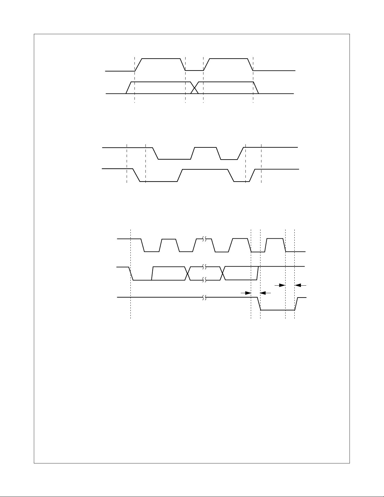
Data Validity (Figure 1)
SCL
FM24C02U/03U – 2K-Bit Standard 2-Wire Bus Interface Serial EEPROM
SDA
DATA STABLE DATA
CHANGE
Start and Stop Definition (Figure 2)
SCL
SDA
START
CONDITION
Acknowledge Response from Receiver (Figure 3)
SCL FROM
MASTER
DATA OUTPUT
FROM
TRANSMITTER
DATA OUTPUT
FROM
RECEIVER
189
STOP
CONDITION
t
AA
t
DH
FM24C02U/03U Rev. A.3
START
CONDITION
ACKNOWLEDGE
PULSE
9
www.fairchildsemi.com
Page 10
FM24C02U/03U – 2K-Bit Standard 2-Wire Bus Interface Serial EEPROM
Acknowledge
The FM24C02U/03U device will always respond with an acknowledge after recognition of a start condition and its slave address. If
both the device and a write operation have been selected, the
FM24C02U/03U will respond with an acknowledge after the
receipt of each subsequent eight bit byte.
In the read mode the FM24C02U/03U slave will transmit eight bits
of data, release the SDA line and monitor the line for an acknowledge. If an acknowledge is detected, FM24C02U/03U will continue
to transmit data. If an acknowledge is not detected,FM24C02U/03U
will terminate further data transmissions and await the stop condition to return to the standby power mode.
Device Addressing
Following a start condition the master must output the address of
the slave it is accessing. The most significant four bits of the slave
address are those of the device type identifier. This is fixed as
1010 for all EEPROM devices.
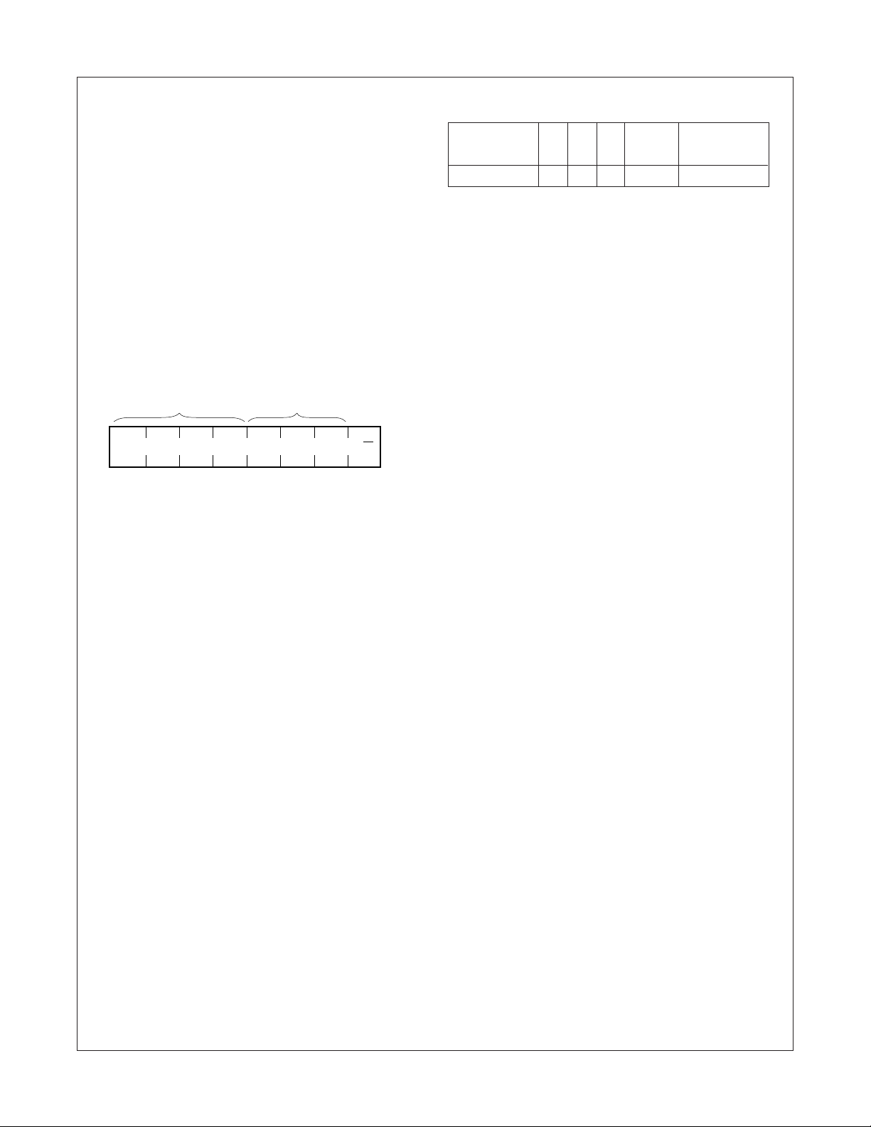
Device Type
Identifier
1 0 1 0 A2 A1 A0 R/W (LSB)
24C02/03
Device
Address
Refer the following table for Slave Addresses string details:
Device A0 A1 A2 Page Page Block
Blocks Addresses
FM24C02U/03U A A A 1 (None)
A: Refers to a hardware configured Device Address pin.
All IIC EEPROMs use an internal protocol that defines a PAGE
BLOCK size of 2K bits (for Word addresses 0x00 through 0xFF).
Therefore, address bits A0, A1, or A2 (if designated 'P') are used
to access a PAGE BLOCK in conjunction with the Word address
used to access any individual data byte.
The last bit of the slave address defines whether a write or read
condition is requested by the master. A '1' indicates that a read
operation is to be executed, and a '0' initiates the write mode.
A simple review: After the FM24C02U/03U recognizes the start
condition, the devices interfaced to the IIC bus wait for a slave
address to be transmitted over the SDA line. If the transmitted
slave address matches an address of one of the devices, the
designated slave pulls the SDA line LOW with an acknowledge
signal and awaits further transmissions.
FM24C02U/03U Rev. A.3
10
www.fairchildsemi.com
Page 11
Write Operations
BYTE WRITE
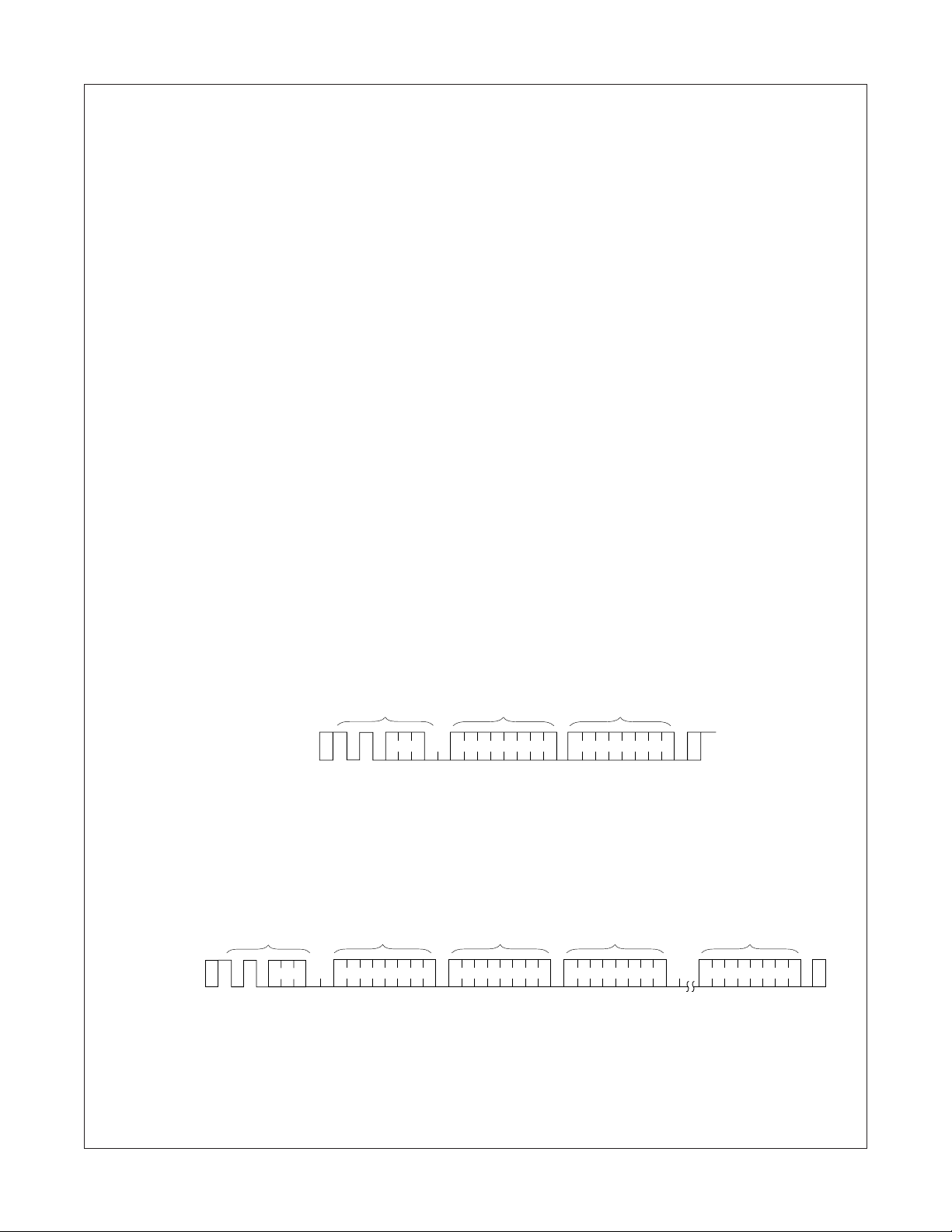
For a write operation, a second address field is required which is a
word address that is comprised of eight bits and provides access to
any one of the 256 bytes in the selected page of memory. Upon
receipt of the byte address, the FM24C02U/03U responds with an
acknowledge and waits for the next eight bits of data, again,
responding with an acknowledge. The master then terminates the
transfer by generating a stop condition at which time the FM24C02U/
03U begins the internal write cycle to the nonvolatile memory. While
the internal write cycle is in progress, the FM24C02U/03U inputs
are disabled, and the device will not respond to any requests from
the master for the duration of tWR. Refer to
acknowledge, and data transfer sequence.
PAGE WRITE
To minimize write cycle time, FM24C02U/03U offer Page Write
feature, by which, up to a maximum of 16 contiguous byte
locations can be programmed all at once (instead of 16 individual
byte writes). To facilitate this feature, the memory array is organized in terms of “Pages.” A Page consists of 16 contiguous byte
locations starting at every 16-Byte address boundary (for example, starting at array address 0x00, 0x10, 0x20 etc.). Page
Write operation limits access to byte locations within a page. In
other words a single Page Write operation will not cross over to
locations on another page but will “roll over” to the beginning of the
page whenever end of Page is reached and additional locations
are continued to be accessed. A Page Write operation can be
initiated to begin at any location within a page (starting address of
the Page Write operation need not be the starting address of a
Page).
Figure 4
for the address,
Page Write is initiated in the same manner as the Byte Write
operation; but instead of terminating the cycle after transmitting
the first data byte, the master can further transmit up to 15 more
bytes. After the receipt of each byte, FM24C02U/03U will respond
with an acknowledge pulse, increment the internal address counter
to the next address, and is ready to accept the next data. If the
master should transmit more than sixteen bytes prior to generating the STOP condition, the address counter will “roll over” and
previously written data will be overwritten. As with the Byte Write
operation, all inputs are disabled until completion of the internal
write cycle. Refer to
Figure 5
for the address, acknowledge, and
data transfer sequence.
Acknowledge Polling
Once the stop condition is issued to indicate the end of the host’s
write operation, the FM24C02U/03U initiates the internal write
cycle. ACK polling can be initiated immediately. This involves
issuing the start condition followed by the slave address for a write
operation. If the FM24C02U/03U is still busy with the write
operation, no ACK will be returned. If the FM24C02U/03U has
completed the write operation, an ACK will be returned and the
host can then proceed with the next read or write operation.
Write Protection (FM24C03U Only)
Programming of the upper half (upper 1Kbit) of the memory will not
take place if the WP pin of the FM24C03U is connected to VCC.
The FM24C03U will respond to slave and byte addresses; but if
the memory accessed is write protected by the WP pin, the
FM24C03U will not generate an acknowledge after the first byte
of data has been received. Thus, the program cycle will not be
started when the stop condition is asserted.
FM24C02U/03U – 2K-Bit Standard 2-Wire Bus Interface Serial EEPROM
Byte Write (Figure 4)
Bus Activity:
Master
SDA Line
Bus Activity:
EEPROM
Page Write (Figure 5)
S
T
SLAVE
Bus Activity:
Master
SDA Line
Bus Activity:
EEPROM
A
R
T
ADDRESS
S
T
A
R
T
A
C
K
SLAVE
ADDRESS
A
C
K
A
C
K
WORD
ADDRESS
S
T
DATA
A
C
K
DATA n + 1DATA nWORD ADDRESS (n)
A
C
K
O
P
A
C
K
S
DATA n + 15
A
C
K
T
O
P
A
C
K
FM24C02U/03U Rev. A.3
11
www.fairchildsemi.com
Page 12
FM24C02U/03U – 2K-Bit Standard 2-Wire Bus Interface Serial EEPROM
Read Operations
Read operations are initiated in the same manner as write
operations, with the exception that the R/W bit of the slave
address is set to a one. There are three basic read operations:
current address read, random read, and sequential read.
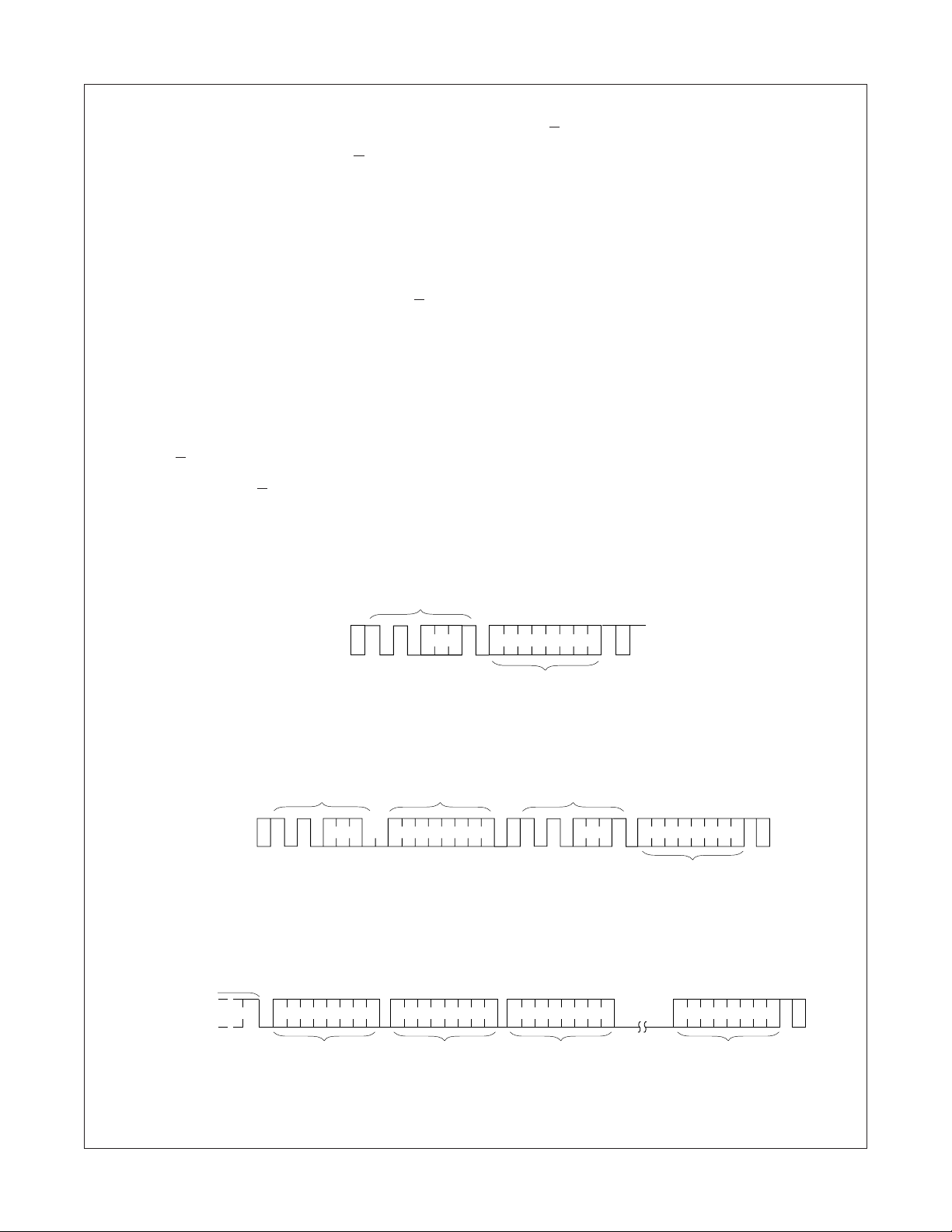
Current Address Read
Internally the FM24C02U/03U contains an address counter that
maintains the address of the last byte accessed, incremented by
one. Therefore, if the last access (either a read or write) was to
address n, the next read operation would access data from
address n + 1. Upon receipt of the slave address with R/W set to
one, the FM24C02U/03U issues an acknowledge and transmits
the eight bit word. The master will not acknowledge the transfer
but does generate a stop condition, and therefore the FM24C02U/
03U discontinues transmission. Refer to
quence of address, acknowledge and data transfer.
Random Read
Random read operations allow the master to access any memory
location in a random manner. Prior to issuing the slave address
with the R/W bit set to one, the master must first perform a
“dummy” write operation. The master issues the start condition,
slave address with the R/W bit set to zero and then the byte
address is read. After the byte address acknowledge, the master
Current Address Read (Figure 6)
Bus Activity:
Master
SDA Line
Bus Activity:
EEPROM
Figure 6
for the se-
S
T
SLAVE
A
ADDRESS
R
T
1 0 1 0 1
immediately issues another start condition and the slave address
with the R/W bit set to one. This will be followed by an acknowledge from the FM24C02U/03U and then by the eight bit word. The
master will not acknowledge the transfer but does generate the
stop condition, and therefore the FM24C02U/03U discontinues
transmission. Refer to
Figure 7
for the address, acknowledge, and
data transfer sequence.
Sequential Read
Sequential reads can be initiated as either a current address read
or random access read. The first word is transmitted in the same
manner as the other read modes; however, the master now
responds with an acknowledge, indicating it requires additional
data. The FM24C02U/03U continues to output data for each
acknowledge received. The read operation is terminated by the
master not responding with an acknowledge or by generating a
stop condition.
The data output is sequential with the data from address n
followed by the data from n + 1. The address counter for read
operations increments all word address bits, allowing the entire
memory contents to be serially read during one operation. After
the entire memory has been read, the counter "rolls over" to the
beginning of the memory. FM24C02U/03U continues to output
data for each acknowledge received. Refer to
address, acknowledge, and data transfer sequence.
S
T
O
P
A
C
K
DATA
NO
A
C
K
Figure 8
for the
Random Read (Figure 7)
Bus Activity:
Master
SDA Line
Bus Activity:
EEPROM
Sequential Read (Figure 8)
Bus Activity:
Master
SDA Line
Bus Activity:
EEPROM
FM24C02U/03U Rev. A.3
Slave
Address
S
T
A
R
T
A
C
K
SLAVE
ADDRESS
A
C
K
A
C
K
WORD
ADDRESS
12
S
T
T
SLAVE
ADDRESS
DATA n + 2DATA n +1DATA n +1
A
DATA n
C
K
A
C
K
DATA n + x
A
R
A
C
K
A
C
K
S
T
O
P
NO
A
C
K
S
T
O
P
NO
A
C
K
www.fairchildsemi.com
Page 13
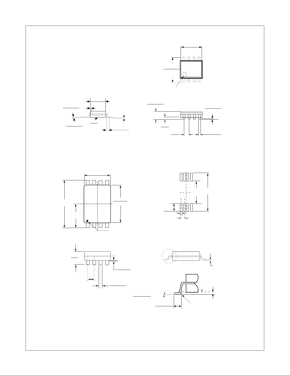
Physical Dimensions inches (millimeters) unless otherwise noted
0.189 - 0.197
(4.800 - 5.004)
8765
0.228 - 0.244
(5.791 - 6.198)
1234
Lead #1
IDENT
FM24C02U/03U – 2K-Bit Standard 2-Wire Bus Interface Serial EEPROM
0.010 - 0.020
(0.254 - 0.508)
0.0075 - 0.0098
(0.190 - 0.249)
Typ. All Leads
0.246 - 0.256
(6.25 - 6.5)
0.123 - 0.128
(3.13 - 3.30)
0.150 - 0.157
(3.810 - 3.988)
x 45¡
0.004
(0.102)
All lead tips
8-Pin Molded Small Outline Package (M8)
0.114 - 0.122
(2.90 - 3.10)
85
14
Pin #1 IDENT
0.053 - 0.069
8¡ Max, Typ.
All leads
0.016 - 0.050
(0.406 - 1.270)
Typ. All Leads
(1.346 - 1.753)
Package Number M08A
0.169 - 0.177
(4.30 - 4.50)
0.004 - 0.010
(0.102 - 0.254)
0.014
(0.356)
(1.78) Typ
(0.42) Typ
0.050
(1.270)
Typ
(0.65) Typ
(4.16) Typ
0.014 - 0.020
(0.356 - 0.508)
(7.72) Typ
Land pattern recommendation
Seating
Plane
Typ.
FM24C02U/03U Rev. A.3
0.0433
Max
(1.1)
See detail A
0¡-8¡
0.0256 (0.65)
Typ.
0.002 - 0.006
(0.05 - 0.15)
0.0075 - 0.0118
(0.19 - 0.30)
DETAIL A
Typ. Scale: 40X
0.020 - 0.028
(0.50 - 0.70)
Notes: Unless otherwise specified
1. Reference JEDEC registration MO153. Variation AA. Dated 7/93
8-Pin Molded Thin Shrink Small Outline Package (MT8)
Package Number MTC08
13
Seating
plane
0.0035 - 0.0079
Gage
plane
0.0075 - 0.0098
(0.19 - 0.25)
www.fairchildsemi.com
Page 14
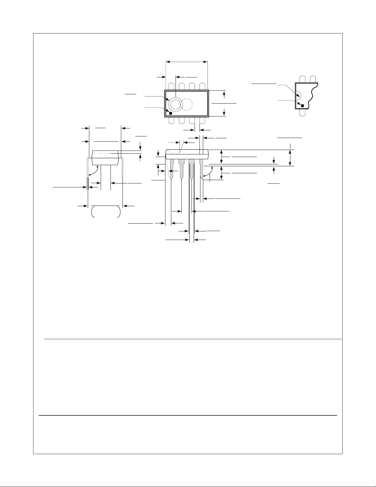
Physical Dimensions inches (millimeters) unless otherwise noted
0.373 - 0.400
(9.474 - 10.16)
0.090
(2.286)
8765
1234
0.040
(1.016)
20° ± 1°
0.065
(1.651)
0.050
(1.270)
+
Typ.
0.250 - 0.005
(6.35 ± 0.127)
0.039
(0.991)
0.130 ± 0.005
(3.302 ± 0.127)
0.125 - 0.140
(3.175 - 3.556)
90° ± 4°
Typ
0.018 ± 0.003
(0.457 ± 0.076)
0.100 ± 0.010
(2.540 ± 0.254)
0.060
(1.524)
95° ± 5°
0.009 - 0.015
(0.229 - 0.381)
0.280
MIN
(7.112)
0.300 - 0.320
(7.62 - 8.128)
+0.040
0.325
-0.015
+1.016
8.255
-0.381
0.092
DIA
(2.337)
Pin #1 IDENT
0.030
(0.762)
0.125
(3.175)
DIA
NOM
0.045 ± 0.015
(1.143 ± 0.381)
Option 1
MAX
0.032 ± 0.005
(0.813 ± 0.127)
RAD
Pin #1
IDENT
0.020
(0.508)
Min
FM24C02U/03U – 2K-Bit Standard 2-Wire Bus Interface Serial EEPROM
87
1
Option 2
0.145 - 0.200
(3.683 - 5.080)
Molded Dual-In-Line Package (N)
Package Number N08E
Life Support Policy
Fairchild's products are not authorized for use as critical components in life support devices or systems without the express written
approval of the President of Fairchild Semiconductor Corporation. As used herein:
1. Life support devices or systems are devices or systems which,
(a) are intended for surgical implant into the body, or (b) support
or sustain life, and whose failure to perform, when properly
used in accordance with instructions for use provided in the
labeling, can be reasonably expected to result in a significant
injury to the user.
Fairchild Semiconductor Fairchild Semiconductor Fairchild Semiconductor Fairchild Semiconductor
Americas Europe Hong Kong Japan Ltd.
Customer Response Center Fax: +44 (0) 1793-856858 8/F, Room 808, Empire Centre 4F, Natsume Bldg.
Tel. 1-888-522-5372 Deutsch Tel: +49 (0) 8141-6102-0 68 Mody Road, Tsimshatsui East 2-18-6, Yushima, Bunkyo-ku
English Tel: +44 (0) 1793-856856 Kowloon. Hong Kong Tokyo, 113-0034 Japan
Français Tel: +33 (0) 1-6930-3696 Tel; +852-2722-8338 Tel: 81-3-3818-8840
Italiano Tel: +39 (0) 2-249111-1 Fax: +852-2722-8383 Fax: 81-3-3818-8841
2. A critical component is any component of a life support device
or system whose failure to perform can be reasonably expected to cause the failure of the life support device or system,
or to affect its safety or effectiveness.
Fairchild does not assume any responsibility for use of any circuitry described, no circuit patent licenses are implied and Fairchild reserves the right at any time without notice to change said circuitry and specifications.
14
FM24C02U/03U Rev. A.3
www.fairchildsemi.com
 Loading...