

Page 1
2211
FIXED DIP DELAY LINE
data
3
TD/TR = 10
(SERIES 2211)
delay
devices, inc.
FEATURES PACKAGES
• High bandwidth (TD/TR =10)
• Low profile
• Epoxy encapsulated
• Meets or exceeds MIL-D-23859C
N/C
N/C
N/C
N/C
N/C
N/C
N/C
N/C
N/C
N/C
GND
1
IN
2
3
4
5
6
7
8
9
10
11
12
24
23
22
21
20
19
18
17
16
15
14
13
N/C
OUT
N/C
N/C
N/C
N/C
N/C
N/C
N/C
N/C
N/C
N/C
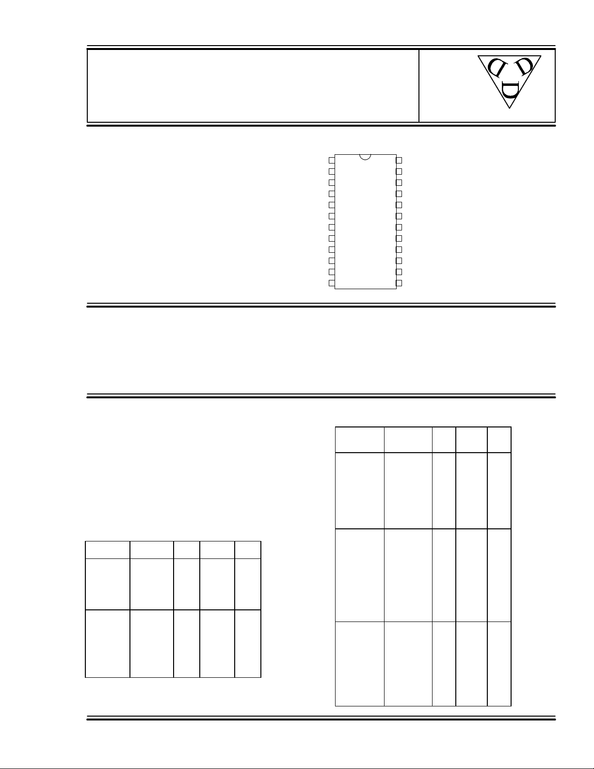
2211-xxz (DIP)
2211-xxzC4 (Gull-Wing)
xx = Delay (TD)
z = Impedance Code
PIN DESCRIPTIONS
IN Signal Input
OUT Signal Output
GND Ground
FUNCTIONAL DESCRIPTION
The 2211-series device is a fixed, single-input, single-output, passive delay line. The signal input (IN) is
reproduced at the output (OUT) with a delay (TD) given by the device dash number. The characteristic
impedance of the line is given by the letter code that follows the dash number (See Table). The rise time
(TR) of the line is 10% of TD, and the 3dB bandwidth is given by 3.5 / TD.
SERIES SPECIFICATIONS
• Dielectric breakdown: 50 Vdc
• Distortion @ output: 10% max.
• Operating temperature: -55°C to +125°C
• Storage temperature: -55°C to +125°C
• Temperature coefficient: 100 PPM/°C
DASH NUMBER SPECIFICATIONS
Part
Number
2211-50A
2211-60A
2211-80A
2211-100A
2211-150A
2211-200A
2211-50B
2211-60B
2211-80B
2211-100B
2211-150B
2211-200B
2211-300B
2211-400B
1997 Data Delay Devices
T
D
(ns)
50.0 ± 2.5
60.0 ± 3.0
80.0 ± 4.0
100 ± 5.0
150 ± 7.5
200 ± 10.0
50.0 ± 2.5
60.0 ± 3.0
80.0 ± 4.0
100 ± 5.0
150 ± 7.5
200 ± 10.0
300 ± 15.0
400 ± 20.0
T
Imped.
R
(ns)
10.0 50 6.0
15.0 50 6.0
20.0 50 7.0
10.0 100 7.0
15.0 100 8.0
20.0 100 8.5
30.0 100 11.0
40.0 100 12.0
(ΩΩ)
5.0 50 3.2
6.0 50 3.6
8.0 50 5.0
5.0 100 6.0
6.0 100 6.0
8.0 100 6.5
R
(ΩΩ)
DC
DASH NUMBER SPECIFICATIONS
Part
Number
2211-40C
2211-80C
2211-120C
2211-200C
2211-300C
2211-400C
2211-500C
2211-600C
2211-800C
2211-50D
2211-100D
2211-150D
2211-200D
2211-250D
2211-300D
2211-400D
2211-500D
2211-600D
2211-800D
2211-1000D
2211-200G
2211-300G
2211-400G
2211-500G
2211-600G
2211-800G
2211-1000G
2211-1200G
2211-1500G
2211-2000G
T
D
(ns)
40.0 ± 2.0
80.0 ± 4.0
120 ± 6.0
200 ± 10.0
300 ± 15.0
400 ± 20.0
500 ± 25.0
600 ± 30.0
800 ± 40.0
50.0 ± 2.5
100 ± 5.0
150 ± 7.5
200 ± 10.0
250 ± 12.5
300 ± 15.0
400 ± 20.0
500 ± 25.0
600 ± 30.0
800 ± 40.0
1000 ± 50.0
200 ± 10.0
300 ± 15.0
400 ± 20.0
500 ± 25.0
600 ± 30.0
800 ± 40.0
1000 ± 50.0
1200 ± 60.0
1500 ± 75.0
2000 ± 100
T
Imped
R
(ns)
4.0 200 7.0
8.0 200 8.0
12.0 200 10.0
20.0 200 13.0
30.0 200 12.0
40.0 200 15.0
50.0 200 17.0
60.0 200 23.0
80.0 200 38.0
5.0 250 7.0
10.0 250 10.0
15.0 250 12.0
20.0 250 22.0
25.0 250 21.0
30.0 250 23.0
40.0 250 26.0
50.0 250 30.0
60.0 250 37.0
80.0 250 41.0
100 250 47.0
20.0 500 20.0
30.0 500 37.0
40.0 500 40.0
50.0 500 45.0
60.0 500 52.0
80.0 500 80.0
100 500 100
120 500 110
150 500 130
200 500 156
(ΩΩ)
R
.
(ΩΩ)
DC
Doc #97027 DATA DELAY DEVICES, INC. 1
2/7/97 3 Mt. Prospect Ave. Clifton, NJ 07013
Page 2

2211
FUNCTIONAL DIAGRAM
1.270±.010
.015 TYP.
.070 MAX.
.018 TYP.
1.280±.020
.020 TYP.
.040 TYP.
.100
.090
1.100
.010±.002
IN OUT
GND
PACKAGE DIMENSIONS
20 19 18 1724 23 22 21
1 2 3 4 5 6 7 8
1.100±.010
11 Equal spaces
each .100±.010
Non-Accumulative
16 15 14 13
.580
MAX.
.010
±.002
1211109
Lead Material:
.280
MAX.
Nickel-Iron alloy 42
TIN PLATE
.600
±.005
DIP (2214-xxz)
131415161718192021222324
.882
±.005
.007
±.005
.050
±.010
1 2 3 4 5 6 7 8 9 10 11 12
.710
±.005
.590
MAX.
.280
MAX.
Gull-Wing (2214-xxzC4)
Doc #97027 DATA DELAY DEVICES, INC. 2
2/7/97 Tel: 973-773-2299 Fax: 973-773-9672 http://www.datadelay.com
Page 3

2211
PASSIVE DELAY LINE TEST SPECIFICATIONS
10%
10%
50%
50%
90%
90%
50%
50%
10%
10%
90%
90%INOUT
OUT
TRIGINTRIG
OSCILLOSCOPE
TEST CONDITIONS
INPUT: OUTPUT:
Ambient Temperature: 25oC ± 3oC R
Input Pulse: High = 3.0V typical C
Low = 0.0V typical Threshold: 50% (Rising & Falling)
Source Impedance: 50Ω Max.
Rise/Fall Time: 3.0 ns Max. (measured
at 10% and 90% levels)
Pulse Width (TD <= 75ns): PWIN = 100ns
Period (TD <= 75ns): PERIN = 1000ns
Pulse Width (TD > 75ns): PWIN = 2 x T
Period (TD > 75ns): PERIN = 10 x T
D
D
NOTE: The above conditions are for test only and do not in any way restrict the operation of the device.
PER
PW
IN
T
RISE
: 10MΩ
load
: 10pf
load
IN
T
FALL
INPUT
SIGNAL
OUTPUT
SIGNAL
PULSE
GENERATOR
R
50 Ω
V
IH
T
RISE
T
RISE
V
OH
Timing Diagram For Testing
IN
DEVICE UNDER
TEST (DUT)
RIN = R
OUT
= Z
LINE
T
FALL
V
IL
T
FALL
V
OL
R
OUT
Test Setup
Doc #97027 DATA DELAY DEVICES, INC. 3
2/7/97 3 Mt. Prospect Ave. Clifton, NJ 07013
 Loading...