

Page 1

Data Sheet (Preliminary)
Conexant Proprietary Information
Doc. No.100444A
December 21, 1999
SmartACFL
Modem
V.90/K56flex/V.34/V.32bis Modem Device Sets with Microcontroller (L2702),
Modem Data Pump (P9373), SmartDAA
(20463), and Optional Voice Codec (20437)
for Low Power Applications
The Conexant SmartACFL V.90/K56flex Modem Device Set with SmartDAA
technology supports analog data up to 56 Kbps, analog fax to 14.4 Kbps,
telephone answering machine (TAM), V.80 synchronous access mode, onboard DSVD, voice/speakerphone (optional), and cellular/GSM operation.
Serial, parallel, or PC Card host interface operation is supported depending on
the selected model (Table 1).
The modem supports ITU-T V.90/K56flex, V.34 and V.32bis data
modulations and is designed to operate with dial-up telephone lines in the U.S.
and worldwide. PC Card and parallel host interface models also support analog
cellular direct connect and GSM direct connect. Low profile, small TQFP
packages and low voltage operation with low power consumption make this
device set ideal for laptop, notebook, and palmtop applications using the
parallel host or serial DTE interface with the MCU, or the PC Card interface
with the MCUP.
The SmartACFL device set consists of a Microcontroller (MCU or MCUP) in a
128-pin TQFP, a Modem Data Pump (MDP) in a 100-pin TQFP, and a Line
Side Device (LSD) (SmartDAA device) in a 32-pin TQFP. The optional Voice
Codec (VC), in a 32-pin TQFP, supports voice/full-duplex speakerphone
(FDSP) operation with interfaces to a microphone and speaker and to a
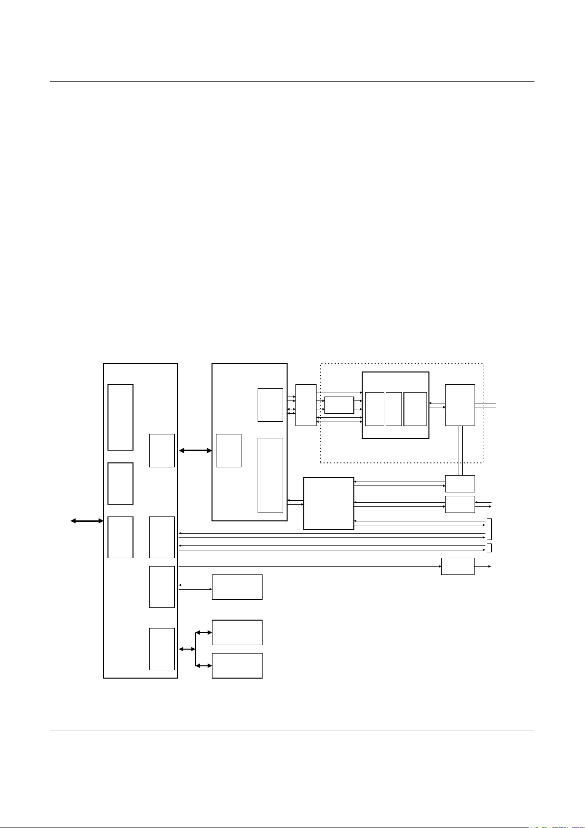
telephone handset/headset. Figure 1 identifies the major hardware signal
interfaces. The MCUP supports two peripheral channels, one channel for the
modem and a second channel for an optional user-defined function
(Function 2).
Conexant's SmartDAA technology (patent pending) eliminates the need for a
costly line transformer, relays, and opto-isolators typically used in discrete DAA
(Data Access Arrangement) implementations. The SmartDAA architecture also
simplifies product implementation by eliminating the need for country-specific
components enabling worldwide homologation of a single modem board design
and a single bill of materials (BOM).
The SmartDAA system-powered DAA operates reliably without drawing power
from the line, unlike line-powered DAAs that operate poorly when line current is
insufficient due to long lines or poor line conditions. Enhanced features, such
as monitoring of local extension status without going off-hook, are also
supported.
Incorporating Conexant’s proprietary Digital Isolation Barrier (DIB) design
(patent pending) and other innovative DAA features, the SmartDAA
architecture simplifies application design, minimizes layout area, and reduces
component cost.
Features
•
V.90 data/V.17 fax modem
•
SmartDAA technology
−
System side powered DAA operates
under poor line current supply
conditions
−
Wake-on-ring
−
Ring detection
−
Line polarity reversal detection
−
Line current loss detection
−
Pulse dialing
−
Call waiting detection
−
Digital PBX line protection
−
Meets world-wide DC VI Masks
requirements
−
Caller ID detection
•
Data/Fax/Voice call discrimination
•
Hardware-based modem controller
•
Hardware-based digital signal
processor (DSP)
•
Voice/full-duplex speakerphone mode
(S models)
•
V.70 DSVD using optional RCDSVD
SCP (S models)
•
World-wide operation
•
Industry standard communication
commands
•
Selectable parallel/serial interface with
speeds up to 230.4 kbps
−
Parallel 16550A UART-compatible
interface
−
Serial ITU-T V.24 (EIA/TIA-232-E)
•
V.80 synchronous access mode
•
Direct mode (serial interface)
•
Synchronous data mode
(serial interface)
•
V.22 bis fast connect
•
Analog cellular direct connect
•
GSM direct connect
•
Sleep mode
•
Thin packages support low profile
designs
•
+3.3V operation with +5V tolerant
digital inputs
Page 2

SmartACFL
V.90/K56flex Modem Device Sets with SmartDAA Technology for Low Power Applications
2
Conexant
Doc. No. 100444A
Proprietary Information
Table 1. SmartACFL Modem Models and Functions
Model/Order/Part Numbers Supported Functions
Marketing Name Device Set
Order No.
MCU
[128-Pin
TQFP]
Part No.
MDP
[100-Pin
TQFP]
Part No.
LSD
[32-Pin
TQFP]
Part No.
Optional
Voice Codec
(VC)
[32-Pin TQFP]
Part No.
V.90/K56fle
x Data
V.34
Data
V.32 bis
Data,
V.17 Fax,
Fax Cl 1,
Fax Cl 2,
TAM,
W-W, V.80
Voice/
FDSP
SmartACFL/56S-PCC DS56-L492-001 L2702-12 P9373-11 20463-11 20437-11 Y Y Y Y
SmartACFL/56-PCC DS56-L492-011 L2702-12 P9373-11 20463-11 — Y Y Y —
SmartACFL/56S DS56-L492-021 L2702-15 P9373-11 20463-11 20437-11 Y Y Y Y
SmartACFL/56 DS56-L492-031 L2702-15 P9373-11 20463-11 — Y Y Y —
Notes:
1. Model options:
S Voice and speakerphone
PCC PC Card host interface (serial DTE/parallel host if not PCC)
56 56 kbps max. rate per V.90
33 33.6 kbps max. rate per V.34
14 14.4 kbps max. rate per V.32bis
2. Supported functions (Y = Supported; — = Not supported):
TAM Telephone answering machine support (handset support requires S model)
Fax Cl 1 and Cl 2 Fax Class 1 and Fax Class 2 support
FDSP Full-duplex speakerphone
Revision History
Revision Date Comments
A 12/21/99 Initial public release of document
Copyright © Conexant Systems, Inc., 1999. All Rights Reserved.
Information in this document is provided in connection with Conexant Systems, Inc. ("Conexant") products. These materials are provided by
Conexant as a service to its customers and may be used for informational purposes only. Conexant assumes no responsibility for errors or
omissions in these materials. Conexant may make changes to specifications and product descriptions at any time, without notice. Conexant
makes no commitment to update the information contained herein. Conexant shall have no responsibility whatsoever for conflicts or
incompatibilities arising from future changes to its specifications and product descriptions.
No license, express or implied, by estoppel or otherwise, to any intellectual property rights is granted by this document. Except as provided in
Conexant’s Terms and Conditions of Sale for such products, Conexant assumes no liability whatsoever.
THESE MATERIALS ARE PROVIDED "AS IS" WITHOUT WARRANTY OF ANY KIND, EITHER EXPRESS OR IMPLIED, RELATING TO
SALE AND/OR USE OF CONEXANT PRODUCTS INCLUDING LIABILITY OR WARRANTIES RELATING TO FITNESS FOR A
PARTICULAR PURPOSE, MERCHANTABILITY, OR INFRINGEMENT OF ANY PATENT, COPYRIGHT OR OTHER INTELLECTUAL
PROPERTY RIGHT. Conexant further does not warrant the accuracy or completeness of the information, text, graphics or other items
contained within these materials. Conexant shall not be liable for any special, indirect, incidental, or consequential damages, including without
limitation, lost revenues or lost profits, which may result from the use of these materials.
Conexant products are not intended for use in medical, life saving or life sustaining applications. Conexant customers using or selling
Conexant products for use in such applications do so at their own risk and agree to fully indemnify Conexant for any damages resulting from
such improper use or sale.
The following are trademarks of Conexant Systems, Inc.: Conexant, the Conexant C symbol, “What’s Next in Communications Technologies”,
SmartDAA, SmartHSF, and SmartACFL. Product names or services listed in this publication are for identification purposes only, and may be
trademarks of third parties. Third-party brands and names are the property of their respective owners.
Reader Response:
Conexant strives to produce quality documentation and welcomes your feedback. Please send
comments and suggestions to [email protected]. For technical questions, contact your local Conexant
sales office or field applications engineer.
Page 3
V.90/K56flex Modem Device Sets with SmartDAA Technology for Low Power Applications SmartACFL
Doc. No. 100444A
Conexant
3
Proprietary Information
Introduction
(continued)
The optional Voice Codec (VC) supports voice/fullduplex speakerphone (FDSP) operation with
interfaces to a microphone and speaker and to a
telephone handset/headset. The optional RCDSVD
Speech Codec Processor (SCP) supports DSVD.
The modem operates by executing firmware from
external 1 Mbit (128k X 8) RAM and 2 Mbit (256k X
8) ROM/Flash ROM. The 33S and 14S models can
alternatively use external 1 Mbit or 2 Mbit
ROM/Flash ROM and the MCU’s internal 32K X 8
RAM. For GSM support the ROM size is doubled.
Accelerator kits and reference designs are available
in electronic form to minimize application design time
and costs. The design package includes schematics,
bill of materials (BOM), board layout files in Gerber
format, and complete documentation. The design is
pretested to pass FCC Part 15, Part 68, and CTR 21
for immediate manufacturing.
Applications
•
PC Cards
•
Embedded systems
•
Serial box modems
•
Set top boxes
•
Point of sales terminals
•
Remote monitoring and data collection systems
Modem Data Pump (MDP)
P9373: 100-Pin TQFP
Voice Codec (VC)
20437: 32-Pin TQFP
(Optional)
SPEAKER
(Mic/Speaker)
Interface
(Optional)
TIP
RING
Electronic
Inductor,
Diode Bridge,
Protection &
EMI,
Impedance
Components
SmartDAA
Interface
Modem
Data Pump
(MDP)
Telephone
Line
Digital Speaker
Circuit (Optional)
PCCard/Parallel/
Serial DTE
Interface
MIC
SPEAKER
MD251F2_FID
SOUNDUCER
Digital
Isolation
Barrier
(DIB)
(OEM
supplied)
Line Side Device (LSD)
20463: 32-Pin TQFP
Line
Side
DIB
Interface
(LSDI)
Codec
Telephone
Line
Interface
DAA Hardware
HS Hybrid
Components
(Optional)
Cellular
Interface
GSM
Interface
RAM
1M (128K x 8)
Central
Processor
Unit (MCU)
SPEAKER
Serial EEPROM
2K (256 x 8) to
32K (4K x 8)
(Optional)
ROM/Flash ROM
2M (256K x 8)
4M (512K X 8)*
* = GSM Support
MCU
Interface
MDP
Interface
Internal
RAM
Serial
EEPROM
Interface
Expansion
Memory
Bus
Interface
Cellular and
GSM
Interface
Host
Interface
Microcontroller Unit (MCU)
L2702: 128-Pin TQFP
Rectifier and
Filter
Components
Figure 1. SmartACFL Modem Major Interfaces
Page 4

SmartACFL
V.90/K56flex Modem Device Sets with SmartDAA Technology for Low Power Applications
4
Conexant
Doc. No. 100444A
Proprietary Information
Detailed Features
General Modem Features
•
Downloadable Architecture
−
Downloadable MCU firmware from the host/DTE
−
Downloadable MDP code modules from the
MCU, transparent to the host
•
V.90 data modem with receive rates up to 56k bps
and send rates up to V.34 rates
−
ITU-T V.90, K56flex, V.34 (33.6 kbps), V.32 bis,
V.32, V.22 bis, V.22, V.23, and V.21; Bell 212A
and 103
−
V.42 LAPM and MNP 2-4 error correction
−
V.42 bis and MNP 5 data compression
−
MNP 10EC™ enhanced cellular performance
−
V.250 (ex V.25 ter) and V.251 (ex V.25 ter
Annex A) commands
•
V.22 bis fast connect
•
Analog cellular direct connect
•
GSM direct connect
•
V.17 fax modem with send and receive rates up to
14.4 kbps
−
ITU-T V.17, V.29, V.27 ter, and V.21 ch. 2
−
EIA/TIA 578 Class 1 and T.30 Class 1.0
commands
•
V.80 synchronous access mode supports hostcontrolled communication protocols with H.324
interface support
•
Data/Fax/Voice call discrimination
•
Hardware-based modem controller
•
Worldwide operation
−
US/Japan/Canada/TBR21 and other countries
−
Caller ID and distinctive ring detection
−
Call progress, blacklisting
•
Telephony/TAM
−
V.253 commands
−
8-bit µ-Law/A-Law coding (G.711)
−
8-bit/16-bit linear coding
−
8 kHz sample rate
−
Concurrent DTMF, ring, and Caller ID detection
•
Full-duplex speakerphone mode (S models)
−
Microphone and speaker interface
−
Telephone handset or headset interface
−
Acoustic and line echo cancellation
−
Microphone gain and muting
−
Speaker volume control and muting
•
PC Card interface (MCUP only) supports two
functions with programmable I/O and window size
•
JTAG Boundary Scan support
•
Built-in host/DTE interface with speeds up to 230.4
kbps
−
Parallel 16550A UART-compatible interface
(MCU)
−
Serial ITU-T V.24 (EIA/TIA-232-E) (MCU)
−
PC Card (MCUP)
•
Flow control and speed buffering
•
Automatic format/speed sensing
•
Serial sync/async data; parallel async data
•
Sleep mode
•
Thin packages support low profile designs (1.6 mm
max. height)
•
MCU (L2702): 128-pin TQFP
•
MDP (P9373): 100-pin TQFP
•
LSD (20463): 32-pin TQFP
•
VC (20437): 32-pin TQFP
Description
General
The SmartACFL device set, comprised of separate
microcontroller (MCU), modem data pump (MDP),
and line side device (LSD) devices, provides the
processing core for a complete modem design. The
optional Voice Codec (VC) supports voice/full-duplex
speakerphone (FDSP) operation with interfaces to a
microphone and speaker and to a telephone
handset/headset (S models). The S model can also
be ordered with an RCDSVD Speech Codec
Processor (SCP) in a 100-pin PQFP to support
DSVD.
Modem operation, including dialing, call progress,
telephone line interface, telephone handset interface,
voice/speakerphone interface, and host interface
functions are supported and controlled through the
V.250, V.251, and V.253-compatible command set.
The modem hardware connects to the host via a
parallel, serial, or PC Card interface. The OEM adds
discrete components as required by the modem
model and the application to complete the system
(Table 1). These components may include a crystal
circuit, EEPROM, DIB components, telephone line
interface, optional voice/speakerphone interface, and
optional cellular/GSM interface.
Parallel interface operation, including cellular and
GSM support, is selected by PARIF input high. Serial
interface operation is selected by PARIF input low.
Cellular operation is selected by LINE/CELL input
low. GSM operation is selected by LINE/GSM input
low.
Page 5

V.90/K56flex Modem Device Sets with SmartDAA Technology for Low Power Applications SmartACFL
Doc. No. 100444A
Conexant
5
Proprietary Information
Data/Fax Modes
In V.90/K56flex data modem mode, the modem can
receive data from a digitally connected central site
modem (CSM) at line speeds up to 56 kbps.
Asymmetrical data transmission supports sending
data up to V.34 rates; this mode can fallback to fullduplex V.34 mode, and to lower rates as dictated by
line conditions.
In V.34 data mode, the modem operates at line
speeds up to 33.6 kbps. Error correction (V.42/MNP
2-4) and data compression (V.42 bis/MNP 5)
maximize data transfer integrity and boost average
data throughput up to 230.4 kbps. Non-errorcorrecting mode is also supported.
Data modem modes perform complete handshake
and data rate negotiations. Using V.34 modulation to
optimize modem configuration for line conditions, the
modem can connect at the highest data rate that the
channel can support from 33600 bps down to 2400
bps with automatic fallback. Automode operation in
V.34 is provided in accordance with PN3320 and in
V.32 bis in accordance with PN2330. All tone and
pattern detection functions required by the applicable
ITU or Bell standard are supported.
In V.32 bis mode, the modem operates at line
speeds up to 14.4 kbps.
In V.22 bis fast connect mode, the modem can
connect at 2400 bps with a very short training time,
which is very efficient for small data transfers.
In fax modem mode, the modem can operate in 2wire, half-duplex, synchronous mode and can
support Group 3 facsimile send and receive speeds
of 14400, 12000, 9600, 7200, 4800, and 2400 bps.
Fax data transmission and reception performed by
the modem are controlled and monitored through the
EIA/TIA-578 Fax Class 1, T.30 Fax Class 1.0, or Fax
Class 2 command interface. Full HDLC formatting,
zero insertion/deletion, and CRC
generation/checking are provided. Both transmit and
receive fax data are buffered within the modem. Data
transfer to and from DTE is flow controlled by
XON/XOFF and RTS/CTS.
Synchronous Access Mode (SAM) - Video
Conferencing
V.80 Synchronous Access Mode between the
modem and the host/DTE is provided for hostcontrolled communication protocols, e.g., H.324
video conferencing applications.
Voice-call-first (VCF) before switching to a
videophone call is also supported.
Worldwide Operation
The modem operates in US/Japan/Canada/TBR21
and other countries. Country dependent parameters
for functions such as dialing, carrier transmit level,
calling tone, call progress tone detection, answer
tone detection, blacklisting, and relay control are
programmable by ConfigurACE II for Windows.
SmartDAA technology allows a single PCB design
and single BOM to be homologated worldwide.
Advanced features such as digital PBX protection
are also supported.
TAM Mode
TAM Mode features include 8-bit µ-Law, A-Law, and
linear coding at 8 kHz sample rate. Full-duplex voice
supports concurrent voice receive and transmit.
Tone detection and generation, call discrimination,
and concurrent DTMF detection are also supported.
ADPCM (4-bit IMA) coding is supported to meet
Microsoft WHQL logo requirements.
TAM Mode is supported by three submodes:
1. Online Voice Command Mode supports
connection to the telephone line or, for the S
model, a handset.
2. Voice Receive Mode supports recording voice or
audio data input from the telephone line or, for
the S model, a microphone/handset.
3. Voice Transmit Mode supports playback of voice
or audio data to the telephone line or, for the S
model, a speaker/handset.
Page 6

SmartACFL
V.90/K56flex Modem Device Sets with SmartDAA Technology for Low Power Applications
6
Conexant
Doc. No. 100444A
Proprietary Information
Voice/Speakerphone Mode (S Models)
S models include additional telephone handset,
external microphone, and external speaker
interfaces that support voice and full-duplex
speakerphone operation.
Hands-free full-duplex telephone operation is
supported in Speakerphone Mode under host
control. Speakerphone Mode features an advanced
proprietary speakerphone algorithm which supports
full-duplex voice conversation with acoustic, line, and
handset echo cancellation. Parameters are
constantly adjusted to maintain stability with
automatic fallback from full-duplex to pseudo-duplex
operation. The speakerphone algorithm allows
position independent placement of microphone and
speaker. The host can separately control volume,
muting, and AGC in microphone and speaker
channels.
V.70 DSVD Mode using RCDSVD SCP Device
(S Models)
On-board DSVD operation requires installation of the
optional RCDSVD SCP (R6715-14). GSM operation
is not available when the RCDSVD SCP is
connected because MCU port PB5 is used for SCP
chip select output (~SVDSEL) rather than address
line A18 output which is needed to support the 4M
ROM.
DSVD provides full-duplex digital simultaneous voice
and data over a single telephone line. DSVD uses
codecs in the RCDSVD SCP to code (compress)
analog speech signals on the RCDSVD LINEIN pin
or MICIN pin for passing to the modem controller in
digitized form. DSVD also decodes (decompresses)
coded speech received from the modem controller
for routing to the RCDSVD LINEOUT pin or
SPKP/SPKN pins in analog form.
DSVD operates in accordance with ITU-T
interoperable G.729 and G.729 Annex A with
interoperable G.729 Annex B. Voice activity
detection supports speech coding at an average bit
rate significantly lower than 8.0 kbps.
DSVD decoder timing recovery algorithm
compensates for clock skew, asynchronous host-todecoder data transfer delay, intervening variable
length data block transmission delay, and loss of
encoded speech data.
The voice interface can be in the form of a headset,
handset or a microphone and speaker (half-duplex
speakerphone). Handset echo cancellation supports
handset use through a hybrid.
In Handset Mode, the RCDSVD SCP interfaces to
the telephone interface circuit using the Line Input
(LINEIN) and Line Out (LINEOUT) lines. In Headset
or Speakerphone Mode, the RCDSVD SCP
interfaces to the audio interface circuit using the
Microphone Input (MICIN) and Speaker out (SPKR)
lines.
GSM (Parallel Host or PC Card Interface)
GSM operation requires installation of 4M (512k x 8)
ROM (56 models) or 2M ROM (33 and 14 models).
ON-board DSVD is not available when the 4 Mbit
ROM is installed since the MCU port PB5 is used for
address line 18 rather than RCDSVD SCP chip
select output (~SVOSEL).
Features supported in GSM operation include:
•
Data modem
−
V.21, V.23, V.22, V.22 bis, V.32
−
ISDN interoperability: 300 bps to 9600 bps
•
Transparent asynchronous mode up to 9600 bps
•
Non-transparent mode (RLP) up to 9600 bps
•
Fax modem send and receive rate up to 9600 bps
•
AT GSM commands (ETSI 07.07)
•
GSM direct connect
•
Firmware interface for OEM-provided phone driver
•
Automatic GSM cable presence detection
•
Built-in parallel host (16550A UART) interface
Sleep Mode
Sleep mode is supported in the modem device set
and the RCDSVD SCP device.
Additional Information
Additional information is described in the SmartACFL
Modem Device Family with SmartDAA Technology
for Low Power Applications Designer’s Guide (Doc.
No. 100446) and the Command Reference Manual
(Doc. No. 100500).
Page 7

V.90/K56flex Modem Device Sets with SmartDAA Technology for Low Power Applications SmartACFL
Doc. No. 100444A
Conexant
7
Proprietary Information
Hardware Description
SmartDAA technology (patent pending) eliminates
the need for a costly analog transformer, relays, and
opto-isolators that are typically used in discrete DAA
implementations. The programmable SmartDAA
architecture simplifies product implementation in
worldwide markets by eliminating the need for
country-specific components.
Microcontroller (MCU/MCUP)
The microcontroller is a Conexant 8-bit
microcomputer with pins to support serial
DTE/parallel host bus/PC Card, MDP, voice/TAM,
speakerphone, and RCDSVD SCP interface
operation. The operating voltage is +3.3V with +5V
tolerant inputs.
The MCUP incorporates a built-in PC Card interface
and CIS memory allowing the MCUP to directly
connect to the PC Card 68-pin socket without
requiring external PICA and CIS devices.
The MCU connects to the DTE/host via a V.24
(EIA/TIA-232-E) serial DTE interface or a parallel
host bus depending on installed firmware, whereas
the MCUP connects to a PC Card socket via built-in
PC Card interface. Unless otherwise stated,
references to general microcontroller functions
include both the MCUP and MCU.
The MCU performs the command processing and
host interface functions. The crystal frequency is
28.224 MHz. The MCU outputs a 28.224 MHz clock
to the MDP eliminating need for a separate MDP
crystal circuit.
The MCU connects to the MDP via dedicated lines
and the external bus. The external bus also connects
to OEM-supplied RAM (56 models), ROM/flash
ROM, and to the optional RCDSVD SCP.
The MCU connects to a serial EEPROM over a
dedicated serial interface.
Two independent functions are supported; the
modem function and an optional user-defined
Function 2. A Card Option Configuration Register
and a Configuration and Status Register for each
function allow independent configuration/control and
status reporting of the respective function.
The MCUP PC Card interface features include:
•
PC Card interface logic and memory
−
Internal 512-byte Card Information Structure
(CIS) provides the tuple information needed to
define the PC Card functionality.
−
CIS Table is configurable from ROM/flash
memory (default) or from NVRAM (option)
−
Address decode logic
•
Modem Function
−
Decoding for standard COM ports in
Overlapping I/O Address Mode
−
Independent I/O Address Mode support
−
Power-down mode control
−
Digital speaker pass-through
−
Supports two ring handling methods
−
Ring Indicate pass-through to Status Change
−
Six 8-bit Modem Function Card Configuration
Registers
Configuration Option Register (full support)
Configuration and Status Register (full support)
Pin Replacement Register (CREADY and
RREADY)
Extended Status Register (RIEvt and RIEnab)
I/O Base Register 0
I/O Base Register 1
•
Optional User-defined Function 2
−
Reset and chip select control
−
Power-down mode control
−
16-bit data transfer control
−
Disable EEPROM control
−
Interrupt request pass through
−
Four 8-bit Card Configuration Registers
Configuration Option Register (full support)
Configuration and Status Register (full support)
I/O Base Register 0
I/O Base Register 1
•
MCU and MCUP packaged in 128-pin TQFP
Page 8

SmartACFL
V.90/K56flex Modem Device Sets with SmartDAA Technology for Low Power Applications
8
Conexant
Doc. No. 100444A
Proprietary Information
RCDSVD Speech Codec Processor (SCP)
(Optional)
The RCDSVD SCP (R6715-14), required for onboard DSVD operation, is packaged in a 100-pin
PQFP. The 56.448 MHz crystal frequency is
supplied by the MDP XCLK output.
MCU/MCUP Firmware
MCU/MCUP firmware performs processing of
general modem control, command sets, data
modem, error correction and data compression
(ECC), fax class 1, fax class 2, DSVD,
voice/audio/TAM/speakerphone, W-class, V.80,
analog cellular, GSM, and serial DTE/parallel
host/PC Card interface functions according to
modem models (Table 1).
Configurations of the modem firmware are provided
to support parallel host bus interface (MCU), serial
DTE interface (MCU) or PC Card interface (MCUP)
operation.
The modem firmware is provided in object code form
for the OEM to program into external ROM/flash
ROM. The modem firmware may also be provided in
source code form under a source code addendum
license agreement.
Modem Data Pump (MDP)
The Modem Data Pump (MDP) supports data/fax
modem, voice record from and playback to the
telephone line, and optional voice/full-duplex
speakerphone operation. The MDP communicates
with the MCU via parallel bus, serial data and clock,
and serial voice (optional) signals. Downloadable
architecture allows upgrading of MDP code from the
MCU.
The MDP, packaged in a 100-pin TQFP, includes a
modem controller interface, a digital signal processor
(DSP), a voice codec (VC) interface, and a
SmartDAA Interface.
The MDP performs telephone line signal
modulation/demodulation in a hardware DSP which
reduces computational load on the host processor.
Downloadable architecture allows updating of MDP
executable code.
The SmartDAA Interface communicates with, and
supplies power and clock to, the LSD through the
DIB.
The input clock frequency is 28.224 MHz and is
supplied by the MCU. The operating voltage is +3.3V
with +5V tolerant inputs.
ADPCM voice processing is supported.
Downloading of MDP code from the MCU is
supported.
Digital Isolation Barrier (DIB) (OEM Supplied)
The DIB electrically DC isolates the MDP from the
LSD. The MDP is connected to a fixed digital ground
and operates with standard CMOS logic levels. The
LSD is connected to a floating ground and can
tolerate high voltage input (compatible with
telephone line and typical surge requirements).
A digital transformer (DXFMR) in the DIB power
channel couples power and clock digital waveforms
from the MDP to the LSD.
The DIB data channel supports bidirectional halfduplex serial transfer of data, control, and status
information between the MDP and the LSD over two
lines.
Page 9

V.90/K56flex Modem Device Sets with SmartDAA Technology for Low Power Applications SmartACFL
Doc. No. 100444A
Conexant
9
Proprietary Information
SmartDAA Line Side Device (LSD)
The LSD includes a Line Side DIB Interface (LSDI),
a coder/decoder (codec), and a Telephone Line
Interface (TLI).
The LSDI communicates with, and receives power
and clock from, the SmartDAA interface in the MDP
through the DIB.
LSD power is received from the top of the DIB
DXFMR secondary winding through a half-wave
rectifying diode and capacitive power filter circuit.
The CLK input is also accepted from the top of the
DXFMR secondary winding through a capacitor and
a resistor in series.
Information is transferred between the LSD and the
MDP through the DIB_P and DIB_N pins. These pins
connect to the MDP DIB_DATAP and DIB_DATAN
pins, respectively, through the DIB.
The TLI integrates DAA and direct telephone line
interface functions and connects directly to the line
TIP and RING pins, as well as to external line
protection components.
Direct LSD connection to TIP and RING allows realtime measurement of telephone line parameters,
such as the telephone central office (CO) battery
voltage and individual telephone line (copper wire)
resistance. Direct LSD connection also allows
dynamic regulation of the off-hook TIP and RING
voltage and total current drawn from the CO. This
allows the modem to maintain compliance with U.S.
and worldwide regulations and to actively control the
DAA power dissipation.
Voice Codec (VC)
The optional VC, packaged in a 32-pin TQFP,
supports voice/full-duplex speakerphone (FDSP)
operation with interfaces to a microphone and
speaker and to a telephone handset/headset.
Page 10
SmartACFL
V.90/K56flex Modem Device Sets with SmartDAA Technology for Low Power Applications
10
Conexant
Doc. No. 100444A
Proprietary Information
MCU/MCUP (L2702) Pinout Diagrams
1
2
3
4
5
6
7
8
9
10
11
12
13
14
15
16
17
18
19
20
21
22
23
24
25
26
27
28
29
30
31
32
33
34
35
36
37
38
102
101
100
99
98
97
96
95
94
93
92
91
90
89
88
87
86
85
84
83
82
81
80
79
78
77
76
75
74
73
72
71
70
69
68
67
66
65
~ROMSEL
~DPSEL
A16
A15
A14
A13
A12
A11
A10
A9
A8
VDD
A7
A6
A5
A4
A3
A2
A1
A0
TDI
TDO
TMS
TRSTP
TCK
GND
D7
D6
D5
D4
D3
D2
D1
D0
~TST
NVMCLK
~RXD
~DPRXD
NC
NC
NC
N
C
NC
~M
R
ES
~RES
NC
NC
NC
NC
NC
NC
~W
R
ITE
~READ
NC
NC
N
C
~DTR
G
N
D
XTLI
VDD
XTLO
G
ND
NC
~STPM
O
DE
~D
SR
~CTS
~R
LSD
~DRSO
U
T
~AAIND
~RI
~TM
~RDL
N
C
~NM
I
~DTR
IND
PD
1
PD2
~AL
~RTS
DPIRQ
~RLY1
~RLY2
~RLY3
~RLY4
LCS
PE5
PARIF
~EXTOH
GND
VGG
DV1TP
CLKOUT
NCNCNCNCNC
RINGD
NVMDATA
~TXD
~TXCLK
~RXCLK/~SCPIRQ
39
40
41
42
43
44
45
46
47
48
49
50
51
52
53
54
55
56
57
58
59
60
61
62
63
64
128
127
126
125
124
123
122
121
120
119
118
117
116
115
114
113
112
111
110
109
108
107
106
105
104
103
1156F3-4 PO-MCU-Ser-128T
NCNCGNDNCNCNCNCNCNCNCNCNCNCNCNCNCPG3
PG2
PG1
PG0
GND
~TMIND
~WKRESOUT
~SCPSEL
A17
~RAMSEL
Figure 2. MCU Pin Signals - Serial DTE Interface 128-Pin TQFP
Page 11
V.90/K56flex Modem Device Sets with SmartDAA Technology for Low Power Applications SmartACFL
Doc. No. 100444A
Conexant
11
Proprietary Information
1
2
3
4
5
6
7
8
9
10
11
12
13
14
15
16
17
18
19
20
21
22
23
24
25
26
27
28
29
30
31
32
33
34
35
36
37
38
102
101
100
99
98
97
96
95
94
93
92
91
90
89
88
87
86
85
84
83
82
81
80
79
78
77
76
75
74
73
72
71
70
69
68
67
66
65
~ROMSEL
~DPSEL
A16
A15
A14
A13
A12
A11
A10
A9
A8
VDD
A7
A6
A5
A4
A3
A2
A1
A0
TDI
TDO
TMS
TRSTP
TCK
GND
D7
D6
D5
D4
D3
D2
D1
D0
~TST
NVMCLK/TXDCLK
GSMTXD
DAA/GSM
N
C
NC
N
C
N
C
NC
~M
R
ES
~R
ES
NC
NC
N
C
N
C
NC
N
C
~W
R
ITE
~READ
N
C
NC
N
C
~HCS
G
N
D
XTLI
VD
D
XTLO
G
ND
NC
~STPM
O
DE
HD
0
H
D1
HD
2
HD3
H
D4
HD
5
H
D6
H
D
7
N
C
~N
M
I
H
A0
H
A1
HA2
~HWT
~HRD
DPIRQ
~RLY1/CTRL0
~RLY2/CTRL1/CTRL0
~RLY3/CELBSY
~RLY4
LCS
CELDATA
PARIF
DAA/CELL or ~EXTOH
GND
VGG
DV1TP
CLKOUT
NCNCNCNCNC
RINGD
NVMDATA
GSMRXD
~CELBSY/RXDCLK
CELCLK/GSMINP0/~SCPIRQ
39
40
41
42
43
44
45
46
47
48
49
50
51
52
53
54
55
56
57
58
59
60
61
62
63
64
128
127
126
125
124
123
122
121
120
119
118
117
116
115
114
113
112
111
110
109
108
107
106
105
104
103
1156F3-5 PO-MCU-Par-128T
NCNCGNDNCNCNCNCNCNCNCNCNCNCNCNCNCPG3
PG2
PG1
PG0
GND
HINT
~WKRESOUT
A18/~SCPSEL
A17
~RAMSEL
Cellular
GSM
RCDSVD
Firmware option
Figure 3. MCU Pin Signals - Parallel Host Interface - 128-Pin TQFP
Page 12
SmartACFL
V.90/K56flex Modem Device Sets with SmartDAA Technology for Low Power Applications
12
Conexant
Doc. No. 100444A
Proprietary Information
1
2
3
4
5
6
7
8
9
10
11
12
13
14
15
16
17
18
19
20
21
22
23
24
25
26
27
28
29
30
31
32
33
34
35
36
37
38
102
101
100
99
98
97
96
95
94
93
92
91
90
89
88
87
86
85
84
83
82
81
80
79
78
77
76
75
74
73
72
71
70
69
68
67
66
65
~ROMSEL
~DPSEL
A16
A15
A14
A13
A12
A11
A10
A9
A8
VDD
A7
A6
A5
A4
A3
A2
A1
A0
TDI
TDO
TMS
TRSTP
TCK
GND
D7
D6
D5
D4
D3
D2
D1
D0
~TST
NVMCLK/TXDCLK
GSMTXD
DAA/GSM
~O
E
~W
E
M
RD
Y
SPKR
IN
RESET
~M
R
ES
PO
R
_R
C
SPKRO
U
T
~IN
PACK
~IR
EQ
R
INT_RC
R
ING
IN
~STSC
HG
~W
R
ITE
~R
EAD
~C
H
2C
S
~IR
EQ
2
~PW
R
D
W
N
2
PD4
G
ND
XTLI
VDD
XTLO
G
N
D
~RESO
U
T2
PD
3
H
D
0
H
D1
H
D2
H
D
3
H
D
4
H
D5
H
D
6
H
D
7
~W
AIT
~N
M
I
H
A0
H
A1
HA2
~IOWR
~IORD
DPIRQ
~RLY1/CTRL0
~RLY2/CTRL1/CTRL0
~RLY3/CELBSY
~RLY4
LCS
CELDATA
PARIF
DAA/CELL or EXTOH
GND
VGG
DV1TP
CLKOUT
~CE2
A0OUT
~IO16E
~IOIS16
~DISEEP
RINGOUT
NVMDATA
GSMRXD
~CELBSY/RXDCLK
CELCLK/GSMINP0/~SCPIRQ
39
40
41
42
43
44
45
46
47
48
49
50
51
52
53
54
55
56
57
58
59
60
61
62
63
64
128
127
126
125
124
123
122
121
120
119
118
117
116
115
114
113
112
111
110
109
108
107
106
105
104
103
1156F3-6 PO-MCUP-128T
~REG
~CE1
GND
HA11
HA10
HA9
HA8
HA7
HA6
HA5
HA4
HA3
HA15
HA14
HA13
HA12
PG3
PG2
PG1
PG0
GND
HINT
READY
A18/~SCPSEL
A17
~RAMSEL
Cellular
GSM
RCDSVD
Firmware option
Figure 4. MCUP Pin Signals - PC Card Interface - 128-Pin TQFP
Page 13

V.90/K56flex Modem Device Sets with SmartDAA Technology for Low Power Applications SmartACFL
Doc. No. 100444A
Conexant
13
Proprietary Information
MDP (P9373) Hardware Pins and Signals
General
The major functional application signals are
summarized below.
System Control and Status
The following discrete signals are used by the host to
control and monitor MDP operation:
•
Wakeup Reset (WKRES#); input
•
Interrupt Request for MDP Interface (IRQ); output
•
Raw Ring (SSD_RING#); output
•
Ring Wake Reset (SSD_RINGWAKE#); output
•
SmartDAA Interrupt for SmartDAA Interface
(SSD_INT); output
Digital Speaker Interface
The following output is used for audible call progress
or carrier monitoring in Data/Fax mode only where
sound quality is not important.
•
Digital Speaker Output (DSPKOUT); output
Host Parallel Bus Interface
The parallel address, data, and control signals are:
•
Address Lines (A[6:0]); input
•
Data Lines (D[7:0]), input/output
•
Chip Select (CS#); input
•
Read Enable (READ#); input
•
Write Enable (WRITE#); output
Host Serial Data Interface
The serial data and clock signals are:
•
Receive Data (RXD); output
•
Receive Data Clock (RXCLK); output
•
Transmit Data (TXD); input
•
Transmit Data Clock (TXCLK); output
Host Serial Voice Interface (S models)
The serial data and clock signals are:
•
Serial Data Out (SI_DD); output
•
Serial Data In (SI_DU); input
•
Serial Shift Clock (SI_CLK); input
•
Sample Shift Clock (SI_FRAME); input
LSD Interface (Through DIB)
The DIB interface signals are:
•
Clock and Power Positive (PWRCLKP); output
•
Clock and Power Negative (PWRCLKN); output
•
Data Positive (DIB_DATAP); input/output
•
Data Negative (DIB_DATAN); input/output
VC Interface
The VC interface signals are:
•
Sleep (IASLEEP); output
•
Master Clock (M_CLK); output
•
Voice Serial Clock (V_SCLK); output
•
Voice Serial Control (V_CTRL); output
•
Voice Serial Frame Sync (V_STROBE); input
•
Voice Serial Transmit Data (V_TXSIN); output
•
Voice Serial Receive Data (V_RXOUT); input
MDP Signal Interface and Pin Assignments
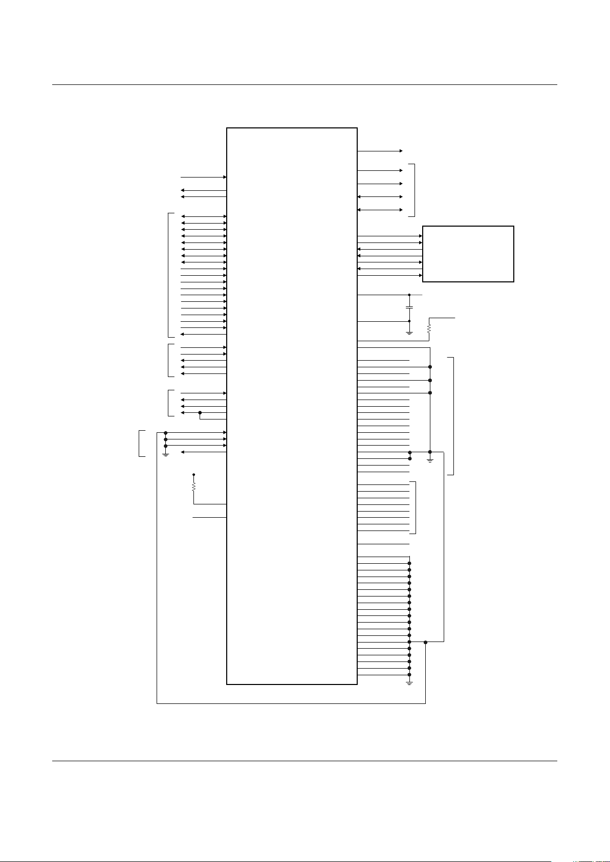
The MDP (P9373) 100-pin TQFP hardware interface
signals are shown in Figure 5.
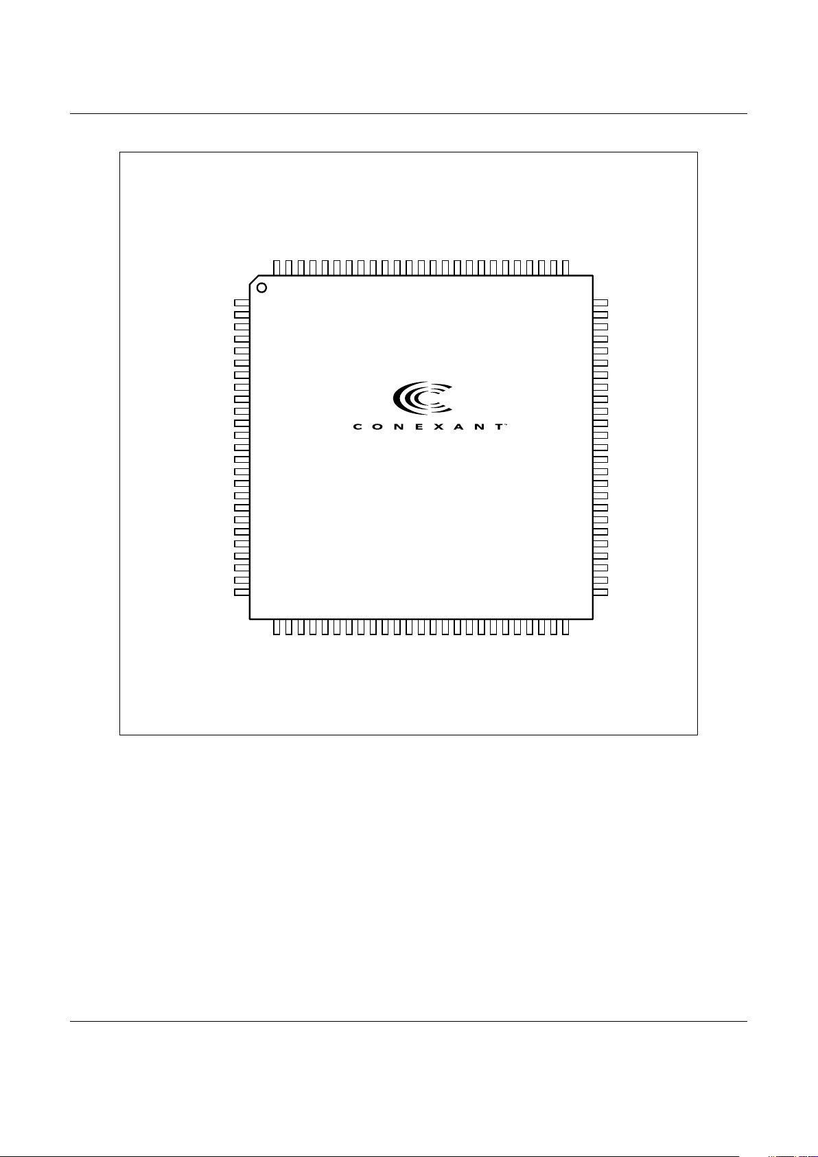
The MDP (P9373) 100-pin TQFP pin signals are
shown in Figure 6.
Page 14
SmartACFL
V.90/K56flex Modem Device Sets with SmartDAA Technology for Low Power Applications
14
Conexant
Doc. No. 100444A
Proprietary Information
CLKIN
XCLK
YCLK
D0 (PC0)
D1 (PC1)
D2 (PC2)
D3 (PC3)
D4 (PC4)
D5 (PC5)
D6 (PC6)
D7 (PC7)
A0 (PD0)
A1 (PD1)
A2 (PD2)
A3 (PD3)
A4 (PD4)
A5
A6
CS# (PD5)
WRITE# (PD6)
READ# (PD7)
IRQ (PB5)
RESET#
WKRES#
SSD_RING#
SSD_RINGWAKE#
SSD_INT
TXD (PA2)
TXCLK (PA3)
RXD (PA6)
RXCLK (PA7)
GP00
SI_FRAME (SA4CLK)
SI_CLK (SR4CLK)
SI_DU (SR8IN)
SI_DD (SR8OUT)
LPO_RC
DDC
48
14
15
67
66
65
64
62
61
60
59
53
52
51
50
49
25
40
55
56
57
35
96
27
95
9
70
36
42
38
44
33
24
23
20
34
84
94
MCU
PARALLEL BUS INTERFACE
DSPKOUT
PWRCLKP
PWRCLKP
DIB_DATAP
DIB_DATAN
IASLEEP
M_CLK (PB0)
V_SCLK (SR2CLK)
V_STROBE (SA2CLK)
V_TXSIN (SR3OUT)
V_RXOUT (SR3IN)
V_CTRL (SR2IO)
PLLVDD
PLLVSS
TESTP
XYCNT
M_CTRL (SR1IO)
M_RXOUT (SR4IN)
M_TXSIN (SR4OUT)
V_CLKIN (IA2CLK)
M_CLKIN (IA1CLK)
M_STROBE (SA1CLK)
PB1
PF6
PF7
GP01
RESERVED
RESERVED
RESERVED
RESERVED
NC
NC
NC
NC
VDD
VDD
VDD
VDD
VDD
VDD
VDD
VDD
VGG
GND
GND
GND
GND
GND
GND
GND
GND
GND
GND
GND
GND
GND
GND
GND
GND
GND
GND
GND
87
92
93
90
89
97
5
3
1
4
2
6
98
99
18
19
100
12
81
29
86
82
78
28
43
30
16
76
77
79
71
72
74
75
7
17
32
45
46
58
69
83
26
8
10
11
13
21
22
31
37
39
41
47
54
63
68
73
80
85
88
91
100444A, fig5, mdp_his_p93_100t
MODEM DATA
PUMP
(MDP)
P9373
100-PIN TQFP
VOICE CODEC
(VC)
20437
32-PIN TQFP
(OPTIONAL)
+3.3V
+3.3V
DIGITAL SPEAKER OUTPUT
DIGITAL
ISOLATION
BARRIER
(DIB)
NC
+5V/+3.3V
MCU
SERIAL VOICE
INTERFACE
MCU
SERIAL DATA AND CLOCK
INTERFACE
MCU
1uF
MCU:CLKOUT
NC
SLEEP
M_CLKIN
M_SCK
M_STROBE
M_TXSIN
M_RXOUT
M_CNTRLSIN
RCDSVD: XTLI (OPTIONAL)
NC
10K
+3.3V
53.6K
VCC
Figure 5. MDP (P9373) 100-Pin TQFP Hardware Interface Signals
Page 15
V.90/K56flex Modem Device Sets with SmartDAA Technology for Low Power Applications SmartACFL
Doc. No. 100444A
Conexant
15
Proprietary Information
MD248F4 PO-HSD-100TQFP
1
2
3
4
5
6
7
8
9
10
11
12
13
14
15
16
17
18
19
20
21
22
23
24
25
26
27
28
29
30
31
32
33
34
35
36
37
38
39
40
41
42
43
44
45
46
47
48
49
50
75
74
73
72
71
70
69
68
67
66
65
64
63
62
61
60
59
58
57
56
55
54
53
52
51
100
99
98
97
96
95
94
93
92
91
90
89
88
87
86
85
84
83
82
81
80
79
78
77
76
V_STROBE (SA2CLK)
V_RXOUT (SR3IN)
V_SCLK (SR2CLK)
V_TXSIN (SR3OUT)
M_CLK (PB0)
V_CTRL (SR2IO)
VDD
GND
SSD_RINGWAKE#
GND
GND
M_RXOUT (SR4IN)
GND
XCLK
YCLK
RESERVED
VDD
TESTP
XYCNT
SI_DU (SR8IN)
GND
GND
SI_CLK (SR4CLK)
SI_FRAME (SA4CLK)
A5
NC
NC
GND
NC
NC
SSD_INT
VDD
GND
D0 (PC0)
D1 (PC1)
D2 (PC2)
D3 (PC3)
GND
D4 (PC4)
D5 (PC5)
D6 (PC6)
D7 (PC7)
VDD
READ# (PD7)
WRITE# (PD6)
CS# (PD5)
GND
A0 (PD0)
A1 (PD1)
A2 (PD2)
M_CTRL (SR1IO)
PLLVSS
PLLVDD
IASLEEP
RESET#
SSD_RING#
DCC
PWRCLKN
PWRCLKP
GND
DIB_DATAP
DIB_DATAN
GND
DSPKOUT
M_CLKIN (IA1CLK)
GND
LPO_RC
VDD
M_STROBE (SA1CLK)
M_TXSIN (SR4OUT)
GND
RESERVED
PB1
RESERVED
RESERVED
VGG
WKRES#
PF6
V_CLKIN (IA2CLK)
GP01
GND
VDD
GP00
SI_DD (SR8OUT)
IRQ (PB5)
TXD (PA2)
GND
RXD (PA6)
GND
A6
GND
TXCLK (PA3)
PF7
RXCLK (PA7)
VDD
VDD
GND
CLKIN
A4 (PD4)
A3 (PD3)
P9373
Figure 6. MDP (P9373) 100-Pin TQFP Pin Signals
Page 16

SmartACFL
V.90/K56flex Modem Device Sets with SmartDAA Technology for Low Power Applications
16
Conexant
Doc. No. 100444A
Proprietary Information
LSD Hardware Pins and Signals
MDP Interface (Through DIB)
The DIB interface signals are:
•
Clock (CLK); input
•
Digital Power (PWR+); input power
•
Digital Ground (DGND); digital ground
•
Data Positive (DIB_P); input
•
Data Negative (DIB_N); input
Telephone Line Interface
The telephone line interface signals are:
•
RING AC Coupled (RAC1); input
•
TIP AC Coupled (TAC1); input
•
Electronic Inductor Resistor (EIR); output
•
TIP and RING DC Measurement (TRDC); input
•
DAC Output Voltage (DAC); output
•
Electronic Inductor Capacitor (EIC)
•
Electronic Inductor Output (EIO)
•
Electronic Inductor Feedback (EIF)
•
Resistive Divider Midpoint (DCF)
•
Transmit Analog Output (TXA); output
•
Receive Analog Input (RXI); input
•
Receiver Gain (RXG); output
•
MOV Enable (MOVEN); output
•
World-wide Impedance 0 (ZW0); input
•
US Impedance 0 (ZUS0); input
•
Transmit Feedback (TXF); input
•
Transmit Output (TXO); output
LSD Signal Interface and Pin Assignments
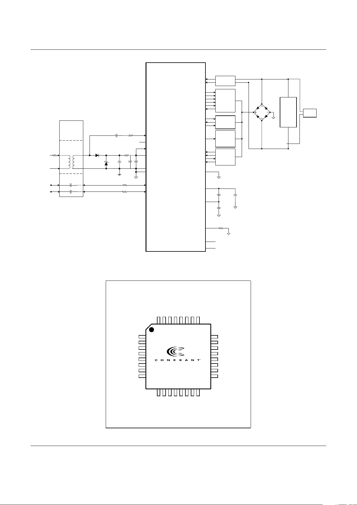
The LSD (20463) 32-pin TQFP hardware interface
signals are shown by major interface in Figure 7.
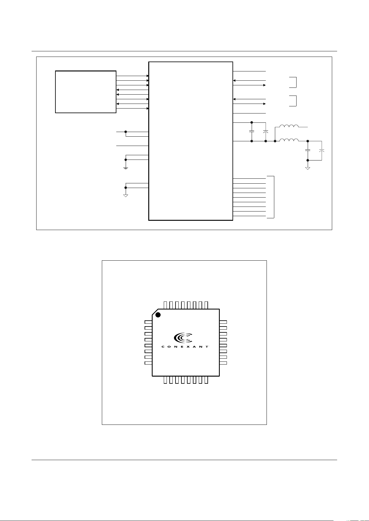
The LSD (20463) 32-pin TQFP pin signals are
shown in Figure 8.
Page 17
V.90/K56flex Modem Device Sets with SmartDAA Technology for Low Power Applications SmartACFL
Doc. No. 100444A
Conexant
17
Proprietary Information
CLK
PWR+
AVDD
DVDD
DGND
AGND
DIB_P
DIB_N
27
31
24
26
25
23
28
29
RAC1
TAC1
EIR
EIC
DAC
TRDC
EIO
EIF
RXG
RXI
TXA
MOVEN (GPIO1)
ZW0
ZUS0
TXO
TXF
DCF
VREF
VC
RBIAS
GPIO2
POR
9
11
15
2
6
5
21
22
4
3
18
32
14
17
20
19
16
8
7
13
1
30
100444A_HIS_20463_Smart ACFL
LINE SIDE DEVICE
(LSD)
20463
32-PIN TQFP
Electronic
Inductor,
Offhook,
Pulse Dial,
and TIP and
RING VI
Control
AGND_LSD
RJ11
Jack
Safety
and
EMI
Protection
AGND_LSD
TIP
RING
Ring In
Filter
AGND_LSD
0.1uF
0.1uF
10 uF
AGND_LSD
Echo
Cancellation
and
Receiver
Impedance
Matching
and
Transmitter
Pulse Dial
Voltage
Protection
(Country
Specific)
GND_LSD
1K
10 pF
0.1uF 0.1uF
1
K
1
K
AGND_LSD
DIGITAL
ISOLATION
BARRIER
(DIB)
PWRCLKP
PWRCLKN
DIB_DATAP
DIB_DATAN
DATA
CHANNEL
10 pF
10 pF
POWER AND
CLOCK
CHANNEL
10
NC
143K
AGND_LSD
VDD
NC
10uF
Figure 7. LSD (20463) 32-Pin TQFP Hardware Interface Signals
MD245F6 PO-20463-32T
1
2
3
4
5
6
7
8
9
10
11
12
13
14
15
16
32
31
30
29
28
27
26
25
24
23
22
21
20
19
18
17
GPIO2
EIC
RXI
RXG
TRDC
DAC
VC
VREF
AVDD
AGND
EIF
EIO
TXO
TXF
TXA
ZUS0
RAC1
RAC2
TAC1
TAC2
RBIAS
ZW0
EIR
DCF
MOVEN (GPIO1)
PWR+
POR
DIB_N
DIB_P
CLK
DVDD
DGND
20463
Figure 8. LSD (20463) 32-Pin TQFP Pin Signals
Page 18

SmartACFL
V.90/K56flex Modem Device Sets with SmartDAA Technology for Low Power Applications
18
Conexant
Doc. No. 100444A
Proprietary Information
VC (20437) Hardware Pins and Signals
(S Models)
General
Microphone and analog speaker interface signals, as
well as telephone handset/head interface signals are
provided to support functions such as speakerphone
mode, telephone emulation, microphone voice
record, speaker voice playback, and call progress
monitor.
Speakerphone Interface
The following signals are supported:
•
Speaker Out (M_SPKR_OUT); analog output Should be used in speakerphone designs where
sound quality is important.
•
Microphone (M_MIC_IN); analog input
Telephone Handset/Headset Interface
•
Telephone Input (M_LINE_IN), input (TELIN) –
Optional connection to a telephone handset a
telephone handset interface circuit.
•
Telephone output (M_LINE_OUTP); output
(TELOUT) - Optional connection to a telephone
handset interface circuit.
•
Center Voltage (VC_HANDSET); output reference
voltage.
MDP Interface
The following interface signals are supported:
•
Reset (POR); input
•
Sleep (SLEEP); input
•
Master Clock (M_CLKIN); input.
•
Serial Clock (M_SCK); output.
•
Control (M_CNTRLSIN); input
•
Serial Frame Sync (M_STROBE); output.
•
Serial Transmit Data (M_TXSIN); input.
•
Serial Receive Data (M_RXOUT); output.
VC Interface Signals and Pin Assignments
The VC (20437) 32-pin TQFP hardware interface
signals are shown by major interface in Figure 9.
The VC (20437) 32-pin TQFP pin signals are shown
in Figure 10.
Page 19
V.90/K56flex Modem Device Sets with SmartDAA Technology for Low Power Applications SmartACFL
Doc. No. 100444A
Conexant
19
Proprietary Information
MD248F7 20437-HIS
VOICE CODEC
(VC)
20437
32-PIN TQFP
AUDIO
CIRCUIT
NC
SPK OUT
MIC
TELIN
TELOUT
MODEM
DATA PUMP
(MSD)
+3.3V
VAA (+3.3V)
1
4
19
21
23
20
22
18
17
25
5
28
26
6
27
IASLEEP
DRESET#
M_CLK
V_SCLK
V_STROBE
V_TXSIN
V_RXOUT
V_CTRL
SLEEP
POR
M_CLKIN
M_SCK
M_STROBE
M_TXSIN
M_RXOUT
M_CNTRLSIN
VDD
VDD
MAVDD
VSS
SET3V_BAR2
MAVSS
VSUB
M_DIG_SPEAKER
M_MIC_IN
M_SPKR_OUT
M_LINE_IN
M_LINE_OUTP
M_LINE_OUTM
VREF
VC
M_MIC_BIAS
M_RELAYA
M_RELAYB
M_ACT90
M_1BIT_OUT
D_LPBK_BAR
NC
NC
NC
2
13
3
14
9
10
11
12
15
24
16
29
30
31
7
8
32
0.1
AGND
10
0.1 10
NC
HANDSET
INTERFACE
NC
AGND
GND
FERRITE
FERRITE
VC_HAND
Figure 9. VC (20437) 32-Pin TQFP Hardware Interface Signals
MD241F8 PO-20437_32T
1
2
3
4
5
6
7
8
9
10
11
12
13
14
15
16
32
31
30
29
28
27
26
25
24
23
22
21
20
19
18
17
SLEEP
M_DIG_SPEAKER
M_SPKR_OUT
POR
MAVDD
MAVSS
NC
NC
M_RELAYA
M_STROBE
M_RXOUT
M_SCK
M_TXSIN
M_CLKIN
M_CNTRLSIN
VDD
M_LINE_OUTP
M_LINE_OUTM
VREF
VC
M_MIC_IN
M_LINE_IN
M_MIC_BIAS
M_RELAYB
NC
D_LPBK_BAR
M_1BIT_OUT
M_ACT90
VSS
VSUB
SET3V_BAR2
VDD
20437
Figure 10. VC (20437) 32-Pin TQFP Pin Signals
Page 20
SmartACFL
V.90/K56flex Modem Device Sets with SmartDAA Technology for Low Power Applications
20
Conexant
Doc. No. 100444A
Proprietary Information
Electrical and Environmental Specifications
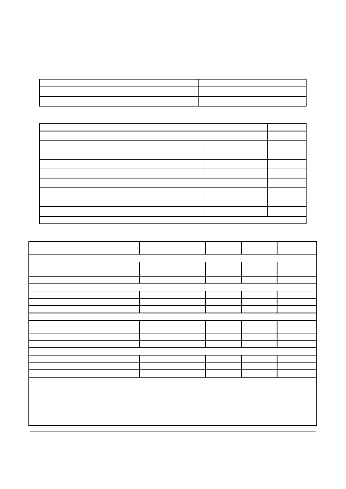
Table 2. Operating Conditions
Parameter Symbol Limits Units
Supply Voltage V
DD
MCU, MDP, VC: +3.0 to +3.6 VDC
Operating Temperature Range T
A
-0 to +70 °C
Table 3. Absolute Maximum Ratings
Parameter Symbol Limits Units
Supply Voltage V
DD
-0.5 to +4.6 VDC
Input Voltage V
IN
-0.5 to (VIO +0.5)* VDC
Storage Temperature Range T
STG
-55 to +125 °C
Analog Inputs V
IN
-0.3 to (VAA + 0.5) VDC
Voltage Applied to Outputs in High Impedance (Off) State V
HZ
-0.5 to (VIO +0.5)* VDC
DC Input Clamp Current I
IK
±20 mA
DC Output Clamp Current I
OK
±20 mA
Static Discharge Voltage (25°C) V
ESD
±2500 VDC
Latch-up Current (25°C) I
TRIG
±400 mA
* VIO = +3.3V ± 0.3V or +5V ± 5%.
Table 4. Current and Power Requirements
Mode
Typ Current
(Ityp) (mA)
Max Current
(Imax) (mA)
Typ Power
(Ptyp) (mW)
Max Power
(Pmax) (mW)
Notes
MCU (L2702-xx)
Normal Mode TBD TBD TBD TBD f = 28.224 MHz
Sleep Mode TBD TBD TBD TBD f = 28.224 MHz
Stop Mode TBD TBD TBD TBD f = 0 MHz
MDP (P9373)
Normal Mode TBD TBD TBD TBD f = 28.224 MHz
Sleep Mode TBD TBD TBD TBD f = 28.224 MHz
Stop Mode TBD TBD TBD TBD f = 0 MHz
LSD (20463)
Normal Mode: Off-hook, normal data
connection
TBD TBD TBD TBD
Normal Mode: On-hook, idle, waiting for ring TBD TBD TBD TBD
Low Power Mode TBD TBD TBD TBD
VC (20437)
Normal Mode TBD TBD TBD TBD
Sleep Mode TBD TBD TBD TBD
Stop Mode TBD TBD TBD TBD
1. Operating voltage: VDD = +3.3V ± 0.3V.
2. Test conditions: VDD = +3.3V for typical values; VDD = +3.6V for maximum values.
3. Input Ripple ≤ 0.1 Vpeak-peak.
4. f = Internal frequency.
5. Stop Mode is the same as Sleep Mode with clocks turned off.
6. Typical current (Ityp) estimated; Max current estimated from Ityp: Imax = Ityp * 1.1.
7. Typical power (Ptyp) computed from Ityp: Ptyp = Ityp * 3.3V; Max power (Pmax) computed from Imax: Pmax = Imax * 3.6V.
Page 21
V.90/K56flex Modem Device Sets with SmartDAA Technology for Low Power Applications SmartACFL
Doc. No. 100444A
Conexant
21
Proprietary Information
Package Dimensions
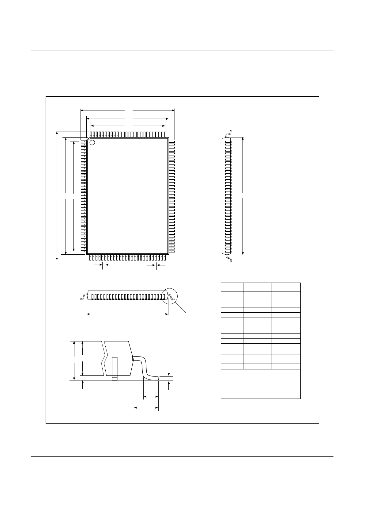
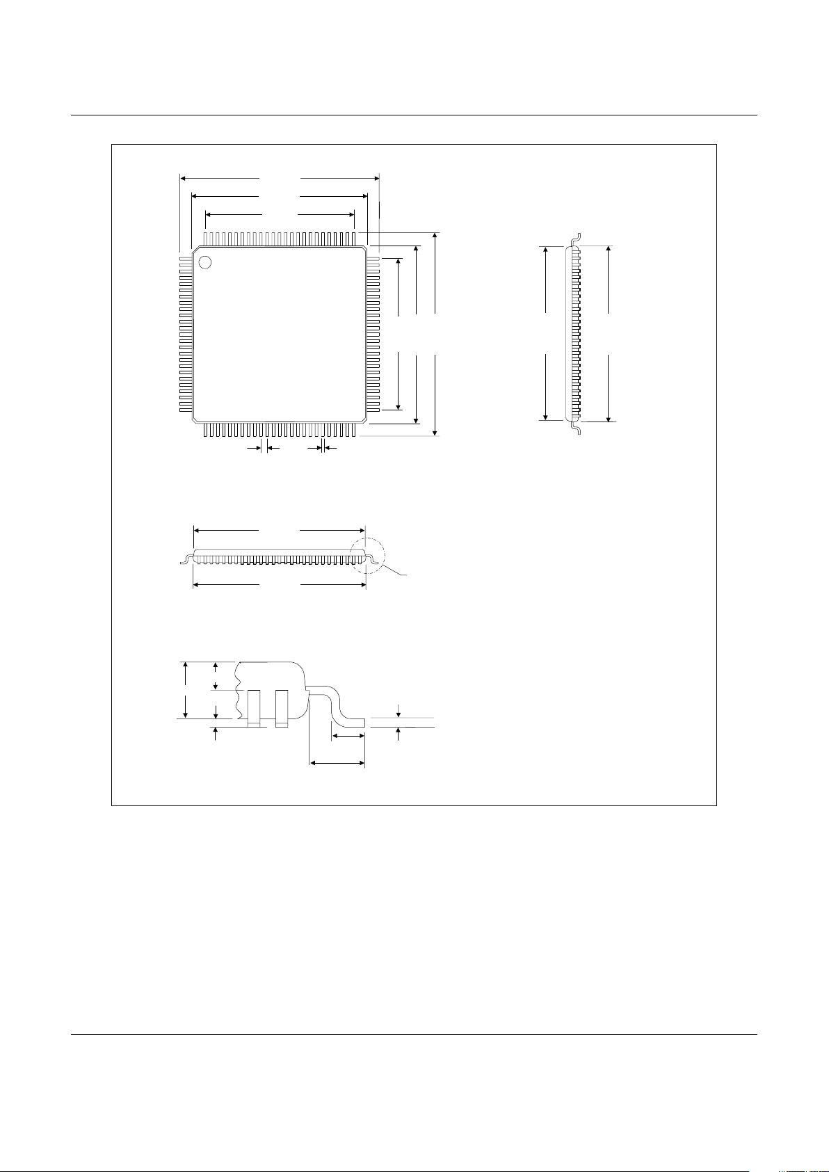
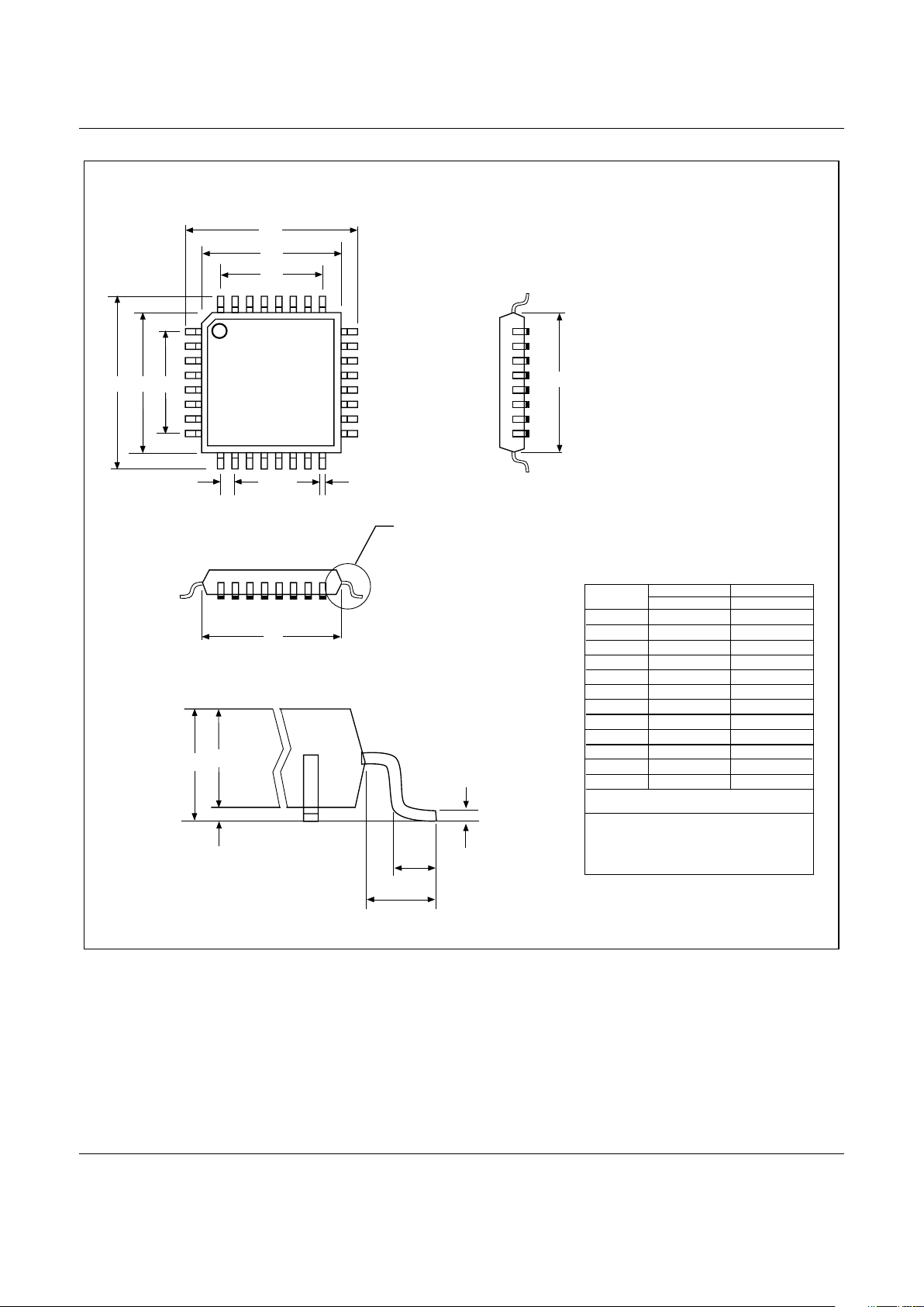
The package dimensions are shown in Figure 11 (128-pin TQFP), Figure 12 (100-pin TQFP) and Figure 13
(32-pin TQFP).
e
b
D
D1
E1
DETAIL A
DETAIL A
A1
L1
c
L
A
E1
E2
E
D2
D1
A2
Millimeters
0.05
21.75
15.75
0.5
0.17
0.11
1.6 MAX
0.15
1.4 REF
22.25
20.0 REF
18.5 REF
16.25
14.0 REF
12.5 REF
0.75
1.0 REF
0.50 BSC
0.27
0.17
0.08 MAX
0.0020
0.8563
0.6201
0.0197
0.0067
0.0043
A
A1
A2
D
D1
D2
E
E1
E2
L
L1
e
b
c
Coplanarity
Min.
Max.
Min.
Max.
Inches
Dim.
Ref: 128-PIN TQFP (GP00-D264)
* Metric values (millimeters) should be used for
PCB layout. English values (inches) are
converted from metric values and may include
round-off errors.
0.0630 MAX
0.0059
0.0551 REF
0.8760
0.7874 REF
0.7283 REF
0.6398
0.5512 REF
0.4921 REF
0.0295
0.0394 REF
0.0197 BSC
0.0106
0.0067
0.0031 MAX
PD-TQFP-128 (040395)
PIN 1
REF
Figure 11. Package Dimensions - 128-Pin TQFP
Page 22
SmartACFL
V.90/K56flex Modem Device Sets with SmartDAA Technology for Low Power Applications
22
Conexant
Doc. No. 100444A
Proprietary Information
DETAIL A
COPLANARITY = 0.08 MAX.
0.60
+0.15, -0.10
0.14 ± .03
16.00 ± 0.15
16.00 ± 0.15
14.00 ± 0.05
12.00 REF
12.00 REF
14.00 ± 0.05
PIN 1
REF
13.87 ± 0.05
14.00 ± 0.05
1.00 REF
1.00 ± .05
0.50 REF
13.87 ± 0.05
14.00 ± 0.05
0.500 BSC
0.22 ± 0.05
Ref. 100-PIN TQFP (GP00-D530)
PD-TQFP-100-D530 (032699)
DETAIL A
0.10 ± .05
Figure 12. Package Dimensions - 100-Pin TQFP
Page 23
V.90/K56flex Modem Device Sets with SmartDAA Technology for Low Power Applications SmartACFL
Doc. No. 100444A
Conexant
23
Proprietary Information
DETAIL A
A1
L1
c
L
A
D1
A2
Millimeters
0.05
8.75
0.5
0.30
0.13
1.6 MAX
0.15
1.4 REF
9.25
7.0 REF
5.6 REF
0.75
1.0 REF
0.80 BSC
0.40
0.19
0.10 MAX
0.0020
0.3445
0.0197
0.0118
0.0051
A
A1
A2
D
D1
D2
L
L1
e
b
c
Coplanarity
Min.
Max.
Min.
Max.
Inches
Dim.
Ref: 32-PIN TQFP (GP00-D262)
* Metric values (millimeters) should be used for
PCB layout. English values (inches) are
converted from metric values and may include
round-off errors.
0.0630 MAX
0.0059
0.0551 REF
0.3642
0.2756 REF
0.2205 REF
0.0295
0.0394 REF
0.0315 BSC
0.0157
0.0075
0.004 MAX
PD-TQFP-32 (040395)
DETAIL A
D1
e
b
D
D2
D1
D1
D
D2
PIN 1
REF
Figure 13. Package Dimensions - 32-Pin TQFP
Page 24

Further Information:
[email protected]
1-800-854-8099 (North America)
33-14-906-3980 (International)
Web Site
www.conexant.com
World Headquarters
Conexant Systems, Inc.
4311 Jamboree Road,
P.O. Box C
Newport Beach, CA 92658-8902
Phone: (949) 483-4600
Fax: (949) 483-6375
U.S. Florida/South America
Phone: (727) 799-8406
Fax: (727) 799-8306
U.S. Los Angeles
Phone: (805) 376-0559
Fax: (805) 376-8180
U.S. Mid-Atlantic
Phone: (215) 244-6784
Fax: (215) 244-9292
U.S. North Central
Phone: (630) 773-3454
Fax: (630) 773-3907
U.S. Northeast
Phone: (978) 692-7660
Fax: (978) 692-8185
U.S. Northwest/Pacific West
Phone: (408) 249-9696
Fax: (408) 249-7113
U.S. South Central
Phone: (972) 733-0723
Fax: (972) 407-0639
U.S. Southeast
Phone: (919) 858-9110
Fax: (919) 858-8669
U.S. Southwest
Phone: (949) 483-9119
Fax: (949) 483-9090
APAC Headquarters
Conexant Systems Singapore,
Pte. Ltd.
1 Kim Seng Promenade
Great World City
#09-01 East Tower
Singapore 237994
Phone: (65) 737 7355
Fax: (65) 737 9077
Australia
Phone: (61 2) 9869 4088
Fax: (61 2) 9869 4077
China
Phone: (86 2) 6361 2515
Fax: (86 2) 6361 2516
Hong Kong
Phone: (852) 2 827 0181
Fax: (852) 2 827 6488
India
Phone: (91 11) 692 4780
Fax: (91 11) 692 4712
Korea - Seoul Office
Phone: (82 2) 565 2880
Fax: (82 2) 565 1440
Korea - Taegu Office
Phone: (82 53) 745-2880
Fax: (82 53) 745-1440
Europe Headquarters
Conexant Systems France
Les Taissounieres B1
1681 Route des Dolines
BP 283
06905 Sophia Antipolis Cedex
France
Phone: (33 1) 41 44 36 50
Fax: (33 1) 93 00 33 03
Europe Central
Phone: (49 89) 829 1320
Fax: (49 89) 834 2734
Europe Mediterranean
Phone: (39 02) 9317 9911
Fax (39 02) 9317 9913
Europe North
Phone: (44 1344) 486 444
Fax: (44 1344) 486 555
Europe South
Phone: (33 1) 41 44 36 50
Fax: (33 1) 41 44 36 90
Middle East Headquarters
Conexant Systems Commercial
(Israel) Ltd.
P.O. Box 12660
Herzlia 46733
Israel
Phone: (972 9) 952 4064
Fax: (972 9) 951 3924
Japan Headquarters
Conexant Systems Japan Co., Ltd.
Shimomoto Bui lding
1-46-3 Hatsudai,
Shibuya-ku
Tokyo, 151-0061
Japan
Phone: (81 3) 5371 1567
Fax: (81 3) 5371 1501
Taiwan Headquar te rs
Conexant Systems, Taiwan Co., Ltd.
Room 2808
International Trade Building
333 Keelung Road, Section 1
Taipei 110
Taiwan, ROC
Phone: (886 2) 2720 0282
Fax: (886 2) 2757 6760
 Loading...