

Page 1
—1—
E93574C8X
Sony reserves the right to change products and specifications without prior notice. This information does not convey any license by
any implication or otherwise under any patents or other right. Application circuits shown, if any, are typical examples illustrating the
operation of the devices. Sony cannot assume responsibility for any problems arising out of the use of these circuits.
Absolute Maximum Ratings (Ta=25 °C)
• Reverse voltage VR 30 V
• Peak reverse voltage VRM 35 V
(RL≥10 kΩ)
• Operating temperature Topr 85 °C
• Storage temperature Tstg –55 to +150 °C
Description
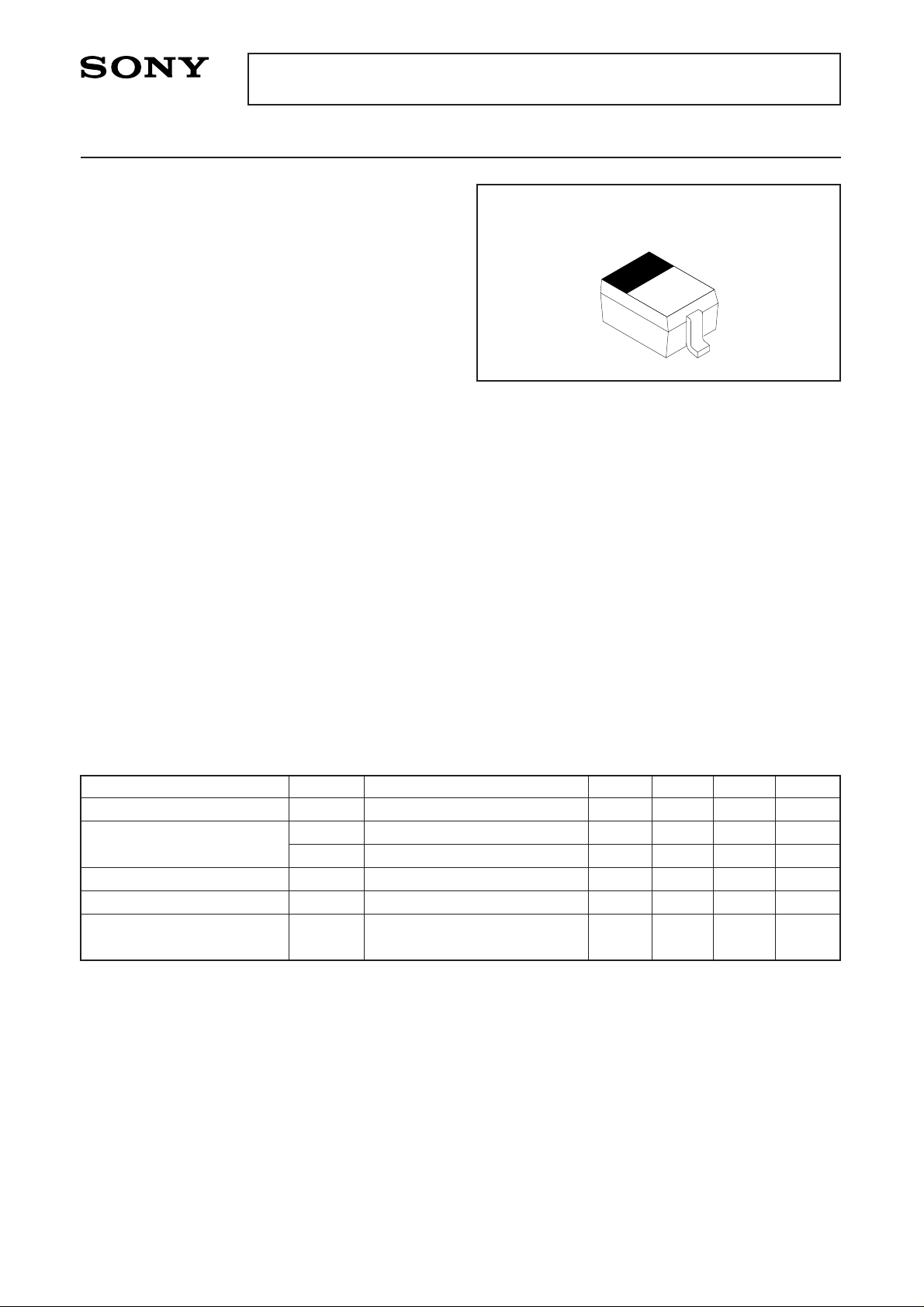
The 1T362A is a variable capacitance diode
designed for electronic tuning of TV tuners and the
super-miniature package allows the tuner
miniaturization.
Features
• Super miniature package
• Low series resistance 0.65 Ω Max. (f=470 MHz)
• Large capacitance ratio 6.5 Typ. (C2/C25)
• Small leakage current 10 nA Max. (VR=28 V)
• Capacitance deviation within 2 %
Applications
Electronic tuning of TV and CATV
Structure
Silicon epitaxial planar type diode
Silicon Variable Capacitance Diode
M-235
1T362A
Electrical Characteristics (Ta=25 °C)
Item
Reverse current
Diode capacitance
Capacitance ratio
Series resistance
Capacitance deviation in a
matching group
Symbol
IR
C2
C25
C2/C25
rs
∆C
Conditions
VR=28 V
VR=2 V, f=1 MHz
VR=25 V, f=1 MHz
f=1 MHz
CD=14 pF, f=470 MHz
VR=2 to 25 V, f=1 MHz
Min. Typ. Max. Unit
10 nA
14.01 15.00 16.33 pF
2.10 2.27 2.39 pF
6.5
0.57 0.65 Ω
2%
∆C:The capacitance deviation of continuous 20 pcs of 1T362A is ranged within 2% in any place of the
taping package.
Page 2
—2—
1T362A
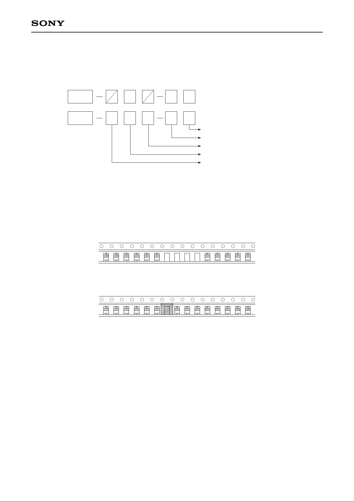
Product Name and Package Specification for the 1T362A.
According to the classification number for the combination of capacitance deviations (hereafter ∆C), assembly
method and automatic mounting equipment section, the following product names are assigned.
Note1) In taping packaging of products groups according to the ∆C classification, products must be divided
according to the group. If taping is performed without grouping into categories, products from two
different groups may be mounted on the same tuner, so that ∆C cannot be assured during tuning,
making tuning defective.
A: Panasert method; Sections are divided by four blank spaces on the carrier tape.
B: Sanyo method; Black tape is affixed to one blank space on the carrier tape to mark sections.
Note 2) ∆C kit number
When taping each group, taping is performed in kit number multiples.
01; Incomplete kit (∆C not guaranteed)
04; 4 kits
20; 20 kits
Recommended kit number; 4 and 20
Other) Minimum number of kits per group is 240 (60 or more at the beginning of the carrier tape). Up
to nine sections on one reel.
Note 3) “MAP” is the method where the neighboring chips are assembled continuously in order to enhance the
concentration of the capacitance deviation in a matching group.
1T362ABase model 04 T8 A
A
1T362ADerived model 20M A T8
Note 1 : Package specification as ordered by customer
∗ Taping direction ∗ T8 only to consolidate specifications
Special selection symbol
Note 2 : ∆C kit number
Note 3 : Assembly method M=MAP
Page 3
—3—
1T362A
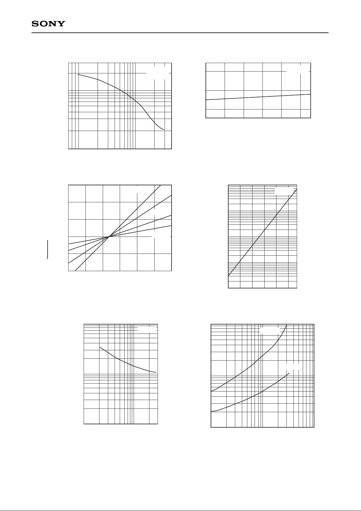
Diode capacitance vs. Reverse voltage
20
10
5
2
1
Diode capacitance (pF)
Reverse voltage (V)
Ta=25°C
f=1MHz
1 2 5 10 20
Diode capacitance vs. Ambient temperature
1.03
1.02
1.01
1.00
0.99
0.98
Ta-Ambient temperature (°C)
VR=1V
f=1MHz
VR=25V
V
R=2V
V
R=10V
–20 0 20 40 60 80 100
Reverse voltage vs. Ambient temperature
50
40
30
VR-Reverse voltage (V)
Ta-Ambient temperature (°C)
IR=10µA
–20 0 20 40 60 80
Diode capacitance
C (Ta)
C (25°C)
Reverse current vs. Ambient temperature
1000
100
10
1
Ta-Ambient temperature (°C)
VR=28V
–20 0 20 40 60 80
IR-Reverse current (pA)
Thermal coefficient of diode capacitance
1000
100
10
1
Thermal coefficient (ppm/°C)
VR-Reverse voltage (V)
10 30
f=1MHz
Reverse current vs. Reverse voltage
100
10
1
1
IR-Reverse current (pA)
VR-Reverse voltage (V)
10 100
Ta=60°C
Ta=25°C
Page 4
SONY CODE
EIAJ CODE
JEDEC CODE
PACKAGE WEIGHT
M-235
∗1.25
+ 0.2
– 0.1
0.3
+ 0.1
– 0.05
∗1.7 ± 0.1
2.5 ± 0.2
1
2
0.3
+ 0.1
– 0.05
∗0.9 ± 0.1
0.2
0 ± 0.05
0° to 10°
0.11
+ 0.1
– 0.06
M-235
0.1g
NOTE: Dimension “∗” does not include mold protrusion.
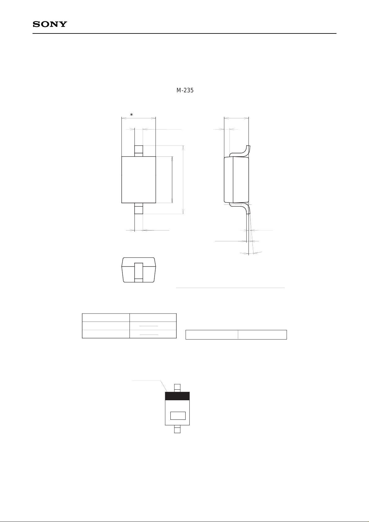
Package Outline Unit : mm
1T362A
—4—
Marking
1
2
CATHODE MARK
62
B
Notes
1) B:Lot No.(Year and Month of manufacture)
Year;Last one digit
Month;A,B,C(for Oct. to Dec.)
1 to 9(for Jan.to Sept.)
 Loading...