

Page 1
1SMC5348 THRU 1SMC5388
FEATURE
S
MECHANICAL DATA
MAXIMUM RATINGS AND ELECTRICAL CHARACTERISTIC
S
D
FSM
STG
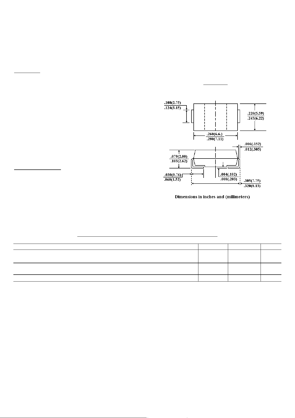
DO-214A
B
SURFACE MOUNT SILICON ZENER DIODE
VOLTAGE - 11 TO 200 Volts Power - 5.0 Watts
l
For surface mounted applications in order to
optimize board space
l
Low profile package
l
Built-in strain relief
l
Glass passivated junction
l
Low inductance
l Typical ID less than 1 £gA above 13V
l
High temperature soldering :
260 ¢J/10 seconds at terminals
l
Plastic package has Underwriters Laboratory
Flammability Classification 94V-O
Case: JEDEC DO-214AB Molded plastic
over passivated junction
Terminals: Solder plated, solderable per
MIL-STD-750, method 2026
Standard Packaging: 16mm tape(EIA-481)
Weight: 0.007 ounce, 0.21 gram
Ratings at 25¢Jambient temperature unless otherwise specified.
SYMBOL VALUE UNITS
DC Power Dissipation @ TL=75 ¢J, Measure at Zero Lead Length(Fig. 1)
Derate above 75¢J(Note 1)
Peak forward Surge Current 8.3ms single half sine-wave superimposed on rated
load(JEDEC Method) (Note 1,2)
Operating Junction and Storage Temperature Range TJ,T
NOTES:
1. Mounted on 8.0mm2 copper pads to each terminal.
2. 8.3ms single half sine-wave, or equivalent square wave, duty cycle = 4 pulses per minute maximum.
P
I
See Fig. 5 Amps
-55 to +150 ¢J
5.0
40.0
Watts
mW/¢J
Page 2
1SMC5348 THRU 1SMC538
8
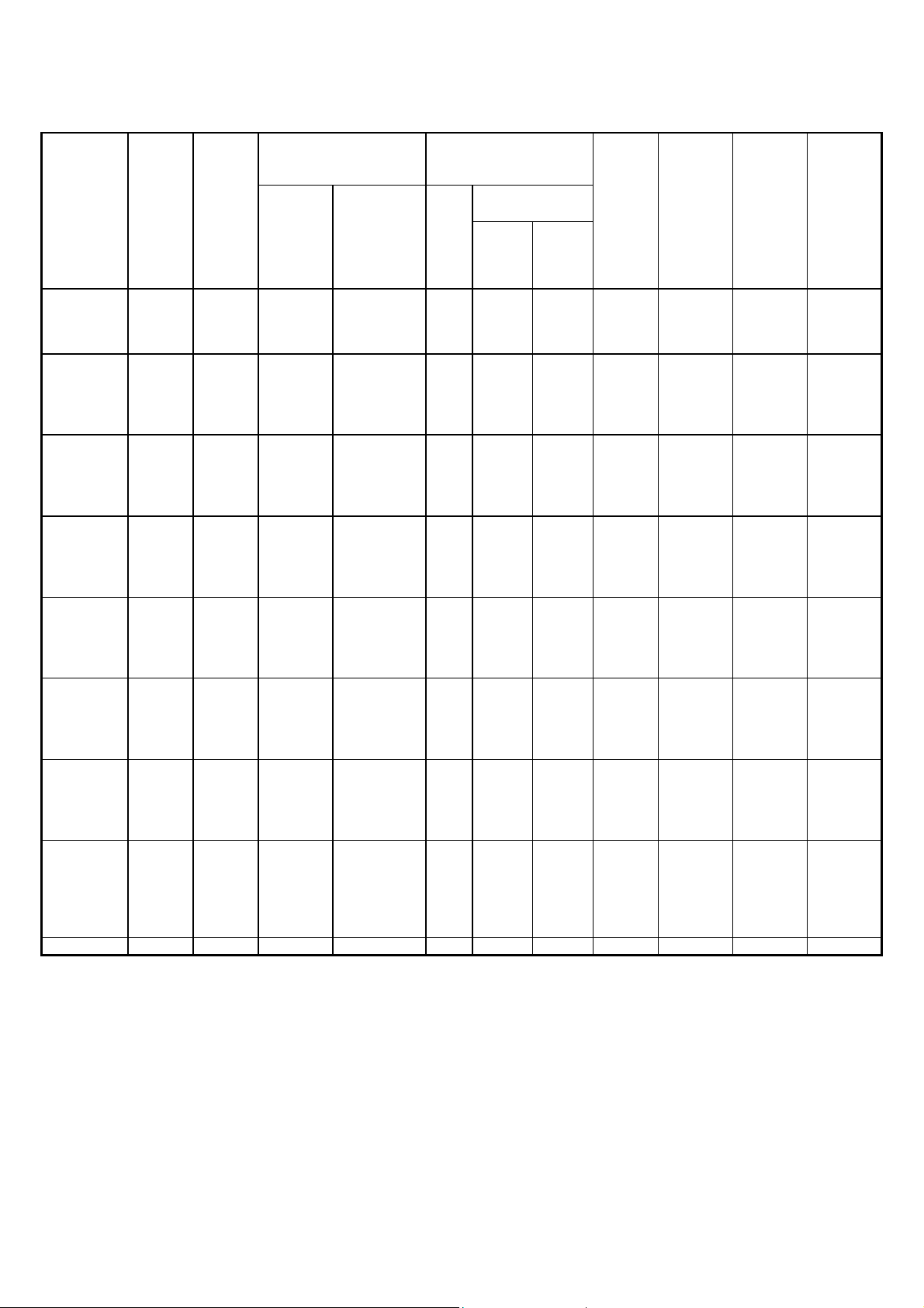
ELECTRICAL CHARACTERISTICS (TA=25¢Junless otherwise noted, VF=1.2 Max @
IF=1A for all types
.
Maximum ZenerImpedanceMax reverseLeakage Curren
t
@ V
R
Volts
Type No.(Note 1.)NominalZener
Voltage
Vz @
I
Z
T
volts(Note 2.)Testcurrent
I
Z
T
m
A
Z
Z
T
@
I
Z
T
Ohms(Note 2.)
Z
Z
k
@
I
Z
K
= 1mAOhms(Note 2.)
I
R
£g
ANon & ASuffixB-Suffi
x
MaxSurg
e
Current
Ir Amps(Note 3.)MaxVoltag
e
Regulatio
n
Vz, Volts(Note 4.)MaximumRegulato
r
Current
I
Z
M
mA(Note 5.)DeviceMarking
Code1SMC534
8
1SMC53491SMC53501SMC535
1
1
1
12131
4
125
100100100
2.5
2.52.52.5
125
1251007
5521188.69.410.
1
8.4
9.19.910.
687.576.7
0.2
5
0.250.250.2
5
430
395365340
348
B
349B350B351B1SMC53521SMC53531SMC535
4
1SMC535
5
1SMC535615161
7
1
8
1975757
0
6
5
652.52.52.5
2.5
3757575
7
5
75110.5
0.5
0.510.811.512.2
1
3
13.711.512.212.
9
13.
7
14.46.365.8
5.5
5.30.250.30.3
5
0.4
0.431529528
0
265
250352B353B354B
355
B
356B1SMC53571SMC535
8
1SMC535
9
1SMC53601SMC5361202
2
2
4
2527655
0
5
0
505033.
5
3.5
45757
5
100
1101200.50.
5
0.5
0.50.514.415.
8
17.
3
1819.415.216.
7
18.
2
1920.65.14.
7
4.4
4.34.10.40.45
0.5
5
0.550.6237216
198
190176357B358
B
359
B
360B361
B
1SMC536
2
1SMC53631SMC53641SMC536
5
1SMC53662
8
30333
6
395
0
40403
0
306
81011
14130
140150160
1700.
5
0.50.50.5
0.520.1
21.623.825.
9
28.121.
2
22.825.127.
4
29.73.9
3.73.53.3
3.10.
6
0.60.60.6
5
0.65170
158144132
122362B
363B364B365
B
366
B
1SMC53671SMC536
8
1SMC536
9
1SMC53701SMC5371434
7
5
1
5660302
5
2
5
2020202
5
2
7
354019021
0
230
2803500.50.
5
0.5
0.50.53133.
8
36.
7
40.34332.735.
8
38.
8
42.645.52.82.
7
2.5
2.32.20.70.
8
0.9
11.211010
0
9
3
8679367B368
B
369
B
370B371
B
1SMC537
2
1SMC53731SMC53741SMC537
5
1SMC53766
2
68758
2
872
0
20201
5
154
2
44456
5
75400
500620720
7600.
5
0.50.50.5
0.544.6
49545
9
6347.
1
51.75662.
2
662.1
21.91.8
1.71.35
1.51.61.8
276
70635
8
54.5372
B
373B374B375
B
376
B
1SMC53771SMC537
8
1SMC537
9
1SMC53801SMC538191100
110
120130151
2
1
2
1010759
0
125
17019076080
0
100
0
115012500.50.
5
0.5
0.50.565.57
2
79.
2
86.493.669.27
6
83.
6
91.298.81.61.
5
1.4
1.31.22.22.
5
2.5
2.52.552.547.
5
4
3
39.536.6377B378
B
379
B
380B381
B
1SMC538
2
1SMC53831SMC53841SMC53851SMC538
6
1SMC5387140
15016017018
0
190
8
888
5
523
0
33035038043
0
4501500
150016501750175
0
18500.5
0.50.50.50.
5
0.510
1
10811512213
0
13710
6
11412212913
7
1441.
2
1.11.11
1
0.92.
5
333
4
534
31.629.42826.
4
25382
B
383B384B385B386
B
387
B
1SMC5388200548018500.51441520.9523.6388
B
£G
NOTE:
1. TOLERANCE AND VOLTAGE DESIGNATION - The JEDEC type numbers shown indicate a tolerance of ¡Ó 10% with
guaranteed limits on only Vz, IR, Ir, and VF as shown in the electrical characteristics table. Units with guaranteed
limits on all seven parameters are indicated by suffix “B” for ¡Ó 5% tolerance.
2. ZENER VOLTAGE (Vz) AND IMPEDANCE (ZZT & ZZK) - Test conditions for Zener voltage and impedance are as
follows; Iz is applied 40 ¡Ó 10 ms prior to reading. Mounting contacts are located from the inside edge of mounting
clips to the body of the diode.(TA=25 ¢J
¡Ï¢·
¡Ð¢±
¢J).
Page 3

3. SURGE CURRENT (Ir) - Surge current is specified as the maximum allowable peak, non-recurrent square-wave
current with a pulse width, PW, of 8.3 ms. The data given in Figure 5 may be used to find the maximum surge
current for a quare wave of any pulse width between 1 ms and 1000ms by plotting the applicable points on
logarithmic paper. Examples of this, using the 6.8v and 200V zeners, are shown in Figure 6. Mounting
contact located as specified in Note 3. (TA=25 ¢J
¡Ï¢·
¡Ð¢±
¢J).
4. VOLTAGE REGULATION (£GVz) - Test conditions for voltage regulation are as follows: Vz measurements are made
at 10% and then at 50% of the Iz max value listed in the electrical characteristics table. The test currents are the
same for the 5% and 10% tolerance devices. The test current time druation for each Vz measurement is 40 ¡Ó 10 ms.
(TA=25 ¢J
¡Ï¢·
¢J). Mounting contact located as specified in Note2.
¡Ð¢±
5. MAXIMUM REGULATOR CURRENT (IZM) - The maximum current shown is based on the maximum voltage of a
5% type unit. Therefore, it applies only to the B-suffix device. The actual IZM for any device may not exceed the
value of 5 watts divided by the actual Vz of the device. TL=75 ¢J at maximum from the device body.
APPLICATION NOTE:
Since the actual voltage available from a given zener
diode is temperature dependent, it is necessary to
determine junction temperature under any set of
operating conditions in order to calculate its value. The
following procedure is recommended:
Lead Temperature, TL, should be determined from:
TL = £cLAPD + T
£c
is the lead-to-ambient thermal resistance (¢J/W)
LA
A
and PD is the power dissipation.
Junction T emperature, TJ , may be found from:
TJ = TL + £GT
JL
£GTJL is the increase in junction temperature above the
lead temperature and may be found from Figure 3 for
a train of power pulses or from Figure 4 for dc power.
£GT
= £cJLP
JL
D
For worst-case design, using expected limits of Iz, limits
of PD and the extremes of TJ(£GTJ) may be estimated.
Changes in voltage, Vz, can then be found from:
£GV = £cVZ£GT
£c
, the zener voltage temperature coefficient, is fount
VZ
J
from Figures 2.
Under high power-pulse operation, the zener voltage will
vary with time and may also be affected significantly be
the zener resistance. For best regulation, keep current
excursions as low as possible.
Data of Figure 3 should not be used to compute surge
capability . Surge limitations are given in Figure 5. They
are lower than would be expected by considering only
junction temperature, as current crowding effects cause
temperatures to be extremely high in small spots resulting
in device degradation should the limits of Figure. 5 be
exceeded.
Page 4
RATING AND CHARACTERISTICS CURVES
TL, LEAD TEMPERATURE (¢J)
0
VZ, ZENER VOLTAGE @IZT (VOLTS
)
D = 0.50.20.10.050.020.01D = 0NOTE BELOW 0.1 SECOND,THERMAL RESPONSECURVE IS APPLICABLE TOANY LEAD LENGTH (L)DUTY CYCLE, D = t1 / t2SINGLE PULS
E£GTJL =£KJL(t)PPKREPETITIVE PULSES£GTJL =£KJL(t,D)PPK
TIME (SECONDS
)
2
L, LEAD LENGTH TO HEAT SINK (INCH
)
NOMINAL VZ(V
)
PD
C
£c
IR
1N5348B THRU 1N5388B
TEMPERATURE COEFFICIENTS
300
200
8
6
4
2
0
, MAXIUMU POWER DISSIPATION (WATTS)
0 20 40 60 80 100 120 140 160
L = LEAD LENGTH TO
(SEE FIGURE 5)
HEAT SINK
100
50
30
20
RANGE
10
£c VZ, TEMPERATURE
OEFFICIENT (mA/¢J_@IZT
5
0 20 40 60 80 100 120 140 160 180 200 22
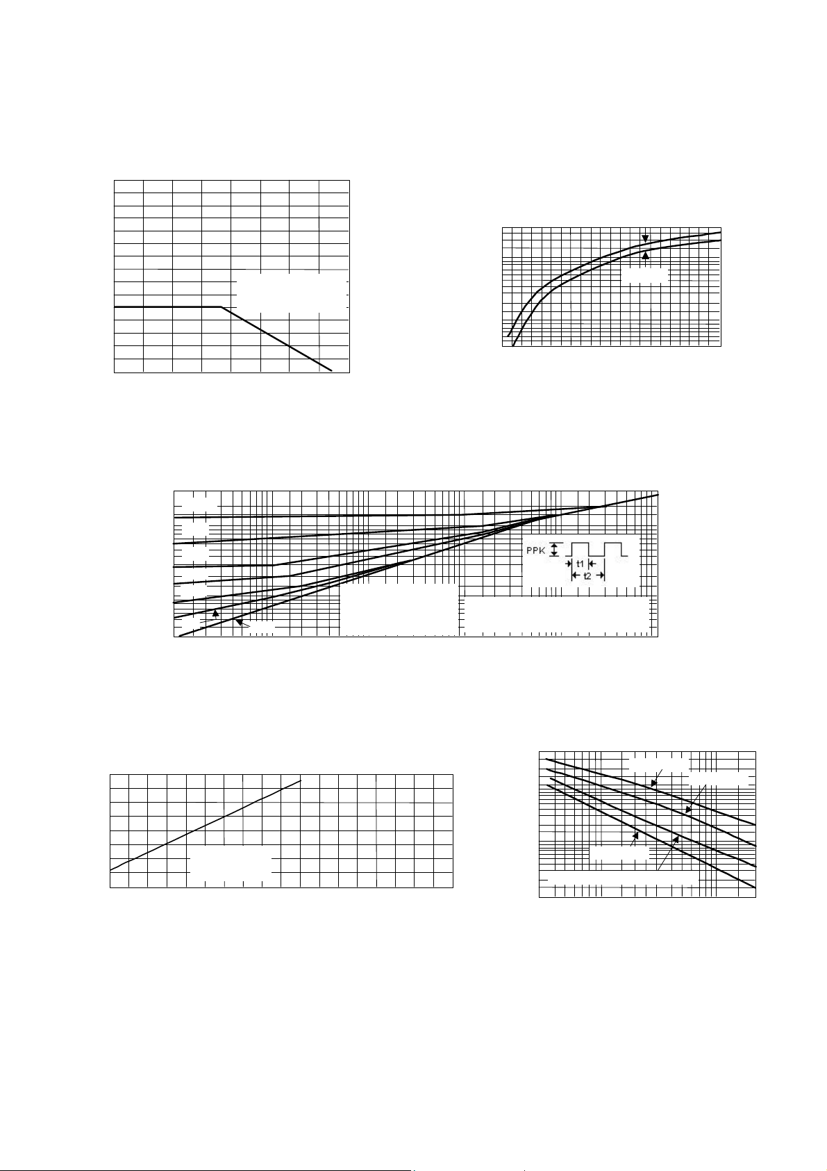
Fig. 1-POWER TEMPERATURE DERATING CURVE Fig. 2-TEMPERATURE COEFFICIENT-RANGE FOR UNITS
6 TO 220 VOLTS
30
20
10
7
5
3
2
LEAD(¢J/W)
1
0.7
JL(t,D), TRANSIENT THERMAL
0.5
RESISTANCE JUNCTION-TO-
0.3
0.0001 0.0002 0.0005 0.001 0.002 0.005 0.01 0.02 0.05 0.1 0.2 0.5 1 2 5 10
Fig. 3-TYPICAL THERMAL RESPONSE
40
40
30
20
10
RESISTANCE (¢J/W)
0
0 0.2
JL, JUNCTION-TO -LEAD THERMAL
MCUNTE ON 8.0mm
COPPER PADS TO
EACH TERMINAL
0.4 0.6
0.8 1
20
10
4
2
1
0.4
0.2
0.1
, PEAK SURGE CURRENT (AMPS)
3 4 6 8 10 20 30 40 60 80 100 200
PW = 1000ms*
SINE / SQUARE WAVE PW = 100ms*
PW = 1ms*
PW = 8.3ms*
Fig. 4-TYPICAL THERMAL RESISTANCE Fig. 5-MAXIMUM NON-REPETITIVE SURGE
CURRENT VERSUS NOMINAL ZENER
VOLT AGE (SEE NOTE 3)
Page 5
RATING AND CHARACTERISTICS CURVES
VZ, ZENER VOLTAGE (VOLTS
)
100
0
VZ, ZENER VOLTAGE (VOLTS)
1000
VZ, ZENER VOLTAGE (VOLTS
)
1N5348B THRU 1N5388B
ZENER VOLTAGE VERSUS ZENER CURRENT
30
20
10
5
2
1
0.5
0.2
0.1
1 10 100 1000
PLOTTED FROM INFORMATION
GIVEN IN FIGURE 6
VZ = 200V
VZ = 6.8V
(FIGURES 7,8, AND 9)
IZ, ZENER CURRENT (mA)
TC = 25
1000
100
10
1
0.1
1 2 3 4 5 6 7 8 9 10
¢J
T = 25
¢J
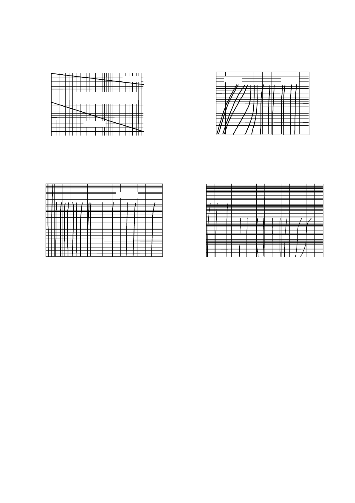
Fig. 6-PEAK SURGE CURRENT VERSUS PULSE
WIDTH(SEE NOTE 3)
T = 25
¢J
100
10
1
IZ, ZENER CURRENT (mA)
0.1
10 20 30 40
70
Fig. 8-ZENER VOLTAGE VERSUS ZENER CURRENT
VZ = 11 THRU 75 VOLTS
Fig. 7-ZENER VOLTAGE VERSUS ZENER CURRENT
VZ = 6.8 THRU 10 VOLTS
100
10
1
IZ, ZENER CURRENT (mA)
0.1
80 100 120 140 160 180 200 220
Fig. 9-ZENER VOLTAGE VERSUS ZENER CURRENT
VZ = 82 THRU 200 VOLTS
*** Data of Figure 3 should not be used to compute surge capability . Surge limitations are given in Figure 5. They are
lower than would be expected by considering only junction temperature, as current crowding effects cause
temperatures to be extremely high in small spots resulting in device degradation should the limits of Figure. 5 be
exceeded
 Loading...