

Page 1

DISCRETE SEMICONDUCTORS
DATA SH EET
ook, halfpage
M3D114
1PS184
High-speed double diode
Product specification
Supersedes data of April 1996
1996 Sep 03
Page 2

Philips Semiconductors Product specification
High-speed double diode 1PS184
FEATURES
• Small plastic SMD package
• High switching speed: max. 4 ns
• Continuous reverse voltage:
max. 80 V
• Repetitive peak reverse voltage:
max. 85 V
• Repetitive peak forward current:
max. 500 mA.
APPLICATIONS
• High-speed switching in e.g.
surface mounted circuits.
DESCRIPTION
The 1PS184 consists of two
high-speed switching diodes with
common cathodes, fabricated in
planar technology, and encapsulated
in the small plastic SMD SC59
package.
21
3
Top view
Marking code: B3T.
Fig.1 Simplified outline (SC59) and symbol.
PINNING
PIN DESCRIPTION
1 anode (a1)
2 anode (a2)
3 common cathode
21
3
MAM084
LIMITING VALUES
In accordance with the Absolute Maximum Rating System (IEC 134).
SYMBOL PARAMETER CONDITIONS MIN. MAX. UNIT
Per diode
V
V
I
RRM
R
F
repetitive peak reverse voltage − 85 V
continuous reverse voltage − 80 V
continuous forward current single diode loaded; see Fig.2;
− 215 mA
note 1
double diode loaded; see Fig.2;
− 125 mA
note 1
I
FRM
I
FSM
repetitive peak forward current − 500 mA
non-repetitive peak forward current square wave; Tj=25°C prior to
surge
t=1µs − 4A
t=1s − 0.5 A
P
tot
T
stg
T
j
total power dissipation T
=25°C; note 1 − 250 mW
amb
storage temperature −65 +150 °C
junction temperature − 150 °C
Note
1. Device mounted on an FR4 printed-circuit board.
1996 Sep 03 2
Page 3

Philips Semiconductors Product specification
High-speed double diode 1PS184
ELECTRICAL CHARACTERISTICS
T
=25°C; unless otherwise specified.
j
SYMBOL PARAMETER CONDITIONS TYP. MAX. UNIT
Per diode
V
F
I
R
C
d
t
rr
V
fr
forward voltage see Fig.3
=1mA 610 − mV
I
F
I
=10mA 740 − mV
F
=50mA − 1.0 V
I
F
I
= 100 mA − 1.2 V
F
reverse current see Fig.4
V
=25V − 30 nA
R
=80V − 0.5 µA
V
R
V
=25V; Tj= 150 °C − 30 µA
R
V
=80V; Tj= 150 °C − 100 µA
R
diode capacitance f = 1 MHz; VR= 0; see Fig.5 − 1.5 pF
reverse recovery time when switched from IF= 10 mA to
− 4ns
IR= 10 mA; RL= 100 Ω;
measured at IR= 1 mA; see Fig.6
forward recovery voltage when switched from IF= 10 mA;
− 1.75 V
tr= 20 ns; see Fig.7
THERMAL CHARACTERISTICS
SYMBOL PARAMETER CONDITIONS VALUE UNIT
R
R
th j-tp
th j-a
thermal resistance from junction to tie-point 250 K/W
thermal resistance from junction to ambient note 1 500 K/W
Note
1. Device mounted on an FR4 printed-circuit board.
1996 Sep 03 3
Page 4
Philips Semiconductors Product specification
High-speed double diode 1PS184
GRAPHICAL DATA
300
I
F
(mA)
200
100
0
0 200
Device mounted on an FR4 printed-circuit board.
single diode loaded
double diode loaded
100
T ( C)
amb
MBD033
o
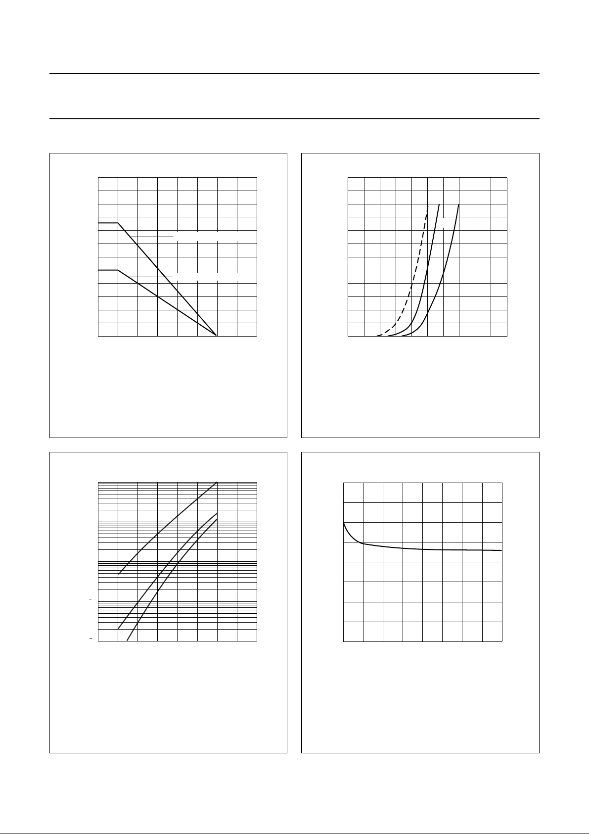
Fig.2 Maximum permissible continuous forward
current as a function of ambient
temperature.
300
handbook, halfpage
I
F
(mA)
200
100
0
02
(1) Tj= 150°C; typical values.
(2) Tj=25°C; typical values.
(3) Tj=25°C; maximum values.
(1) (3)(2)
1
MBG382
VF (V)
Fig.3 Forward current as a function of forward
voltage.
2
10
handbook, halfpage
I
R
(µA)
10
1
1
10
2
10
(1) VR= 80 V; maximum values.
(2) VR= 80 V; typical values.
(3) VR= 25 V; typical values.
(1) (2) (3)
0
100
Tj (
MBG380
o
C)
Fig.4 Reverse current as a function of junction
temperature.
200
0.8
handbook, halfpage
C
d
(pF)
0.6
0.4
0.2
0
0816124
f = 1 MHz; Tj=25°C.
MBG446
VR (V)
Fig.5 Diode capacitance as a function of reverse
voltage; typical values.
1996 Sep 03 4
Page 5

Philips Semiconductors Product specification
High-speed double diode 1PS184
handbook, full pagewidth
R = 50SΩ
V = V I x R
RF S
(1) IR= 1 mA.
I
F
D.U.T.
SAMPLING
OSCILLOSCOPE
R = 50iΩ
MGA881
t
r
10%
V
R
90%
t
p
input signal
Fig.6 Reverse recovery voltage test circuit and waveforms.
t
I
F
t
rr
t
(1)
output signal
I
R = 50SΩ
Ω1 k Ω450
D.U.T.
I
OSCILLOSCOPE
R = 50iΩ
MGA882
Fig.7 Forward recovery voltage test circuit and waveforms.
1996 Sep 03 5
10%
t
r
90%
t
p
input
signal
V
V
fr
t
t
output
signal
Page 6
Philips Semiconductors Product specification
High-speed double diode 1PS184
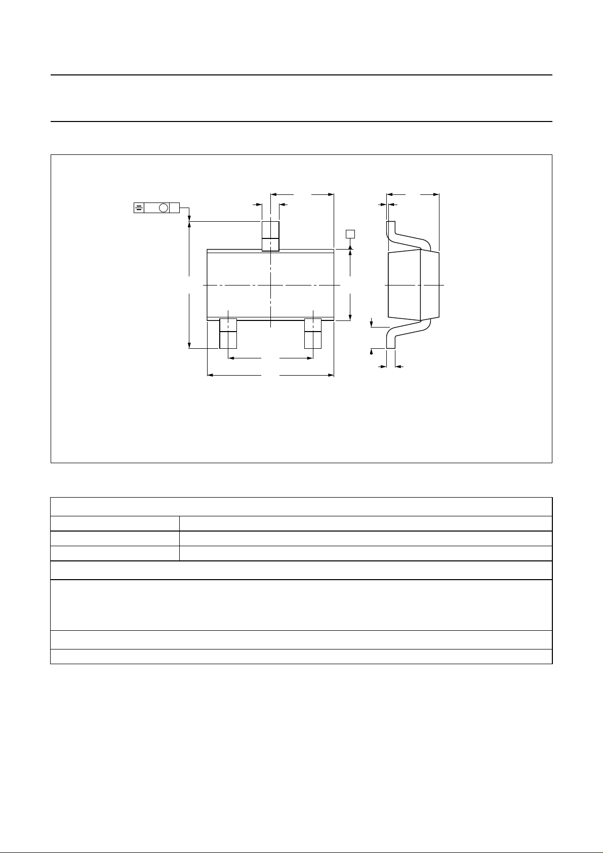
PACKAGE OUTLINE
handbook, full pagewidth
Dimensions in mm.
0.2
1.65
2.1
1.7
3.1
2.7
1.25
3
2
AM
3.0
2.5
0.50
0.35
1
0.100
0.013
A
1.7
1.3
0.6
0.2
MSA313 - 1
1.3
1.0
0.26
0.10
Fig.8 SC59.
DEFINITIONS
Data Sheet Status
Objective specification This data sheet contains target or goal specifications for product development.
Preliminary specification This data sheet contains preliminary data; supplementary data may be published later.
Product specification This data sheet contains final product specifications.
Limiting values
Limiting values given are in accordance with the Absolute Maximum Rating System (IEC 134). Stress above one or
more of the limiting values may cause permanent damage to the device. These are stress ratings only and operation
of the device at these or at any other conditions above those given in the Characteristics sections of the specification
is not implied. Exposure to limiting values for extended periods may affect device reliability.
Application information
Where application information is given, it is advisory and does not form part of the specification.
LIFE SUPPORT APPLICATIONS
These products are not designed for use in life support appliances, devices, or systems where malfunction of these
products can reasonably be expected to result in personal injury. Philips customers using or selling these products for
use in such applications do so at their own risk and agree to fully indemnify Philips for any damages resulting from such
improper use or sale.
1996 Sep 03 6
 Loading...