

Page 1
查询1PS10SB62供应商
DISCRETE SEMICONDUCTORS
DATA SH EET
M3D891
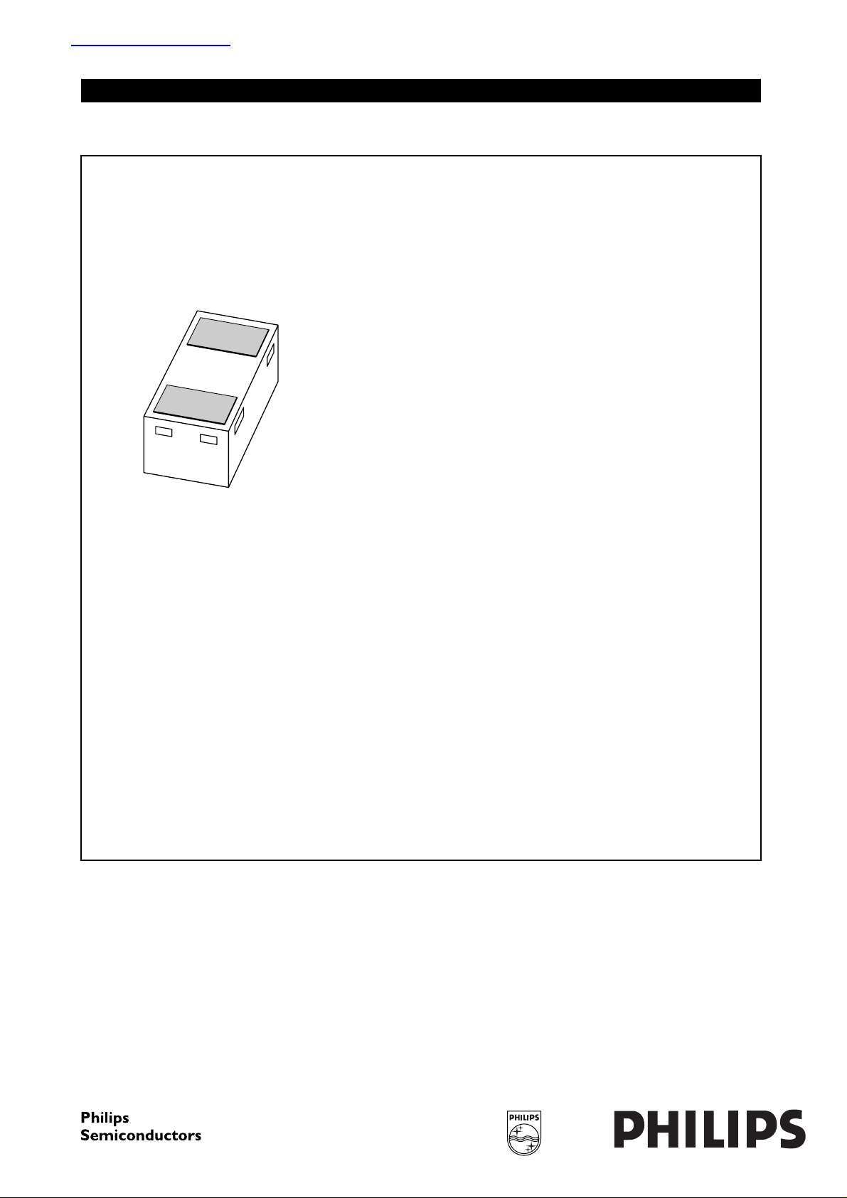
BOTTOM VIEW
1PS10SB62
Schottky barrier diode
Product specification 2003 May 15
Page 2
Philips Semiconductors Product specification
Schottky barrier diode 1PS10SB62
FEATURES
• Ultra high switching speed
• Very low capacitance
• High breakdown voltage
DESCRIPTION
An epitaxial Schottky barrier diode encapsulated in a
SOD882 leadless ultra small plastic package.
ESD sensitive device, observe handling precautions.
• Leadless ultra small plastic package
(1 mm × 0.6 mm × 0.5 mm)
• Boardspace 1.17 mm2 (approx. 10% of SOT23)
handbook, halfpage
• Power dissipation comparable to SOT23.
APPLICATIONS
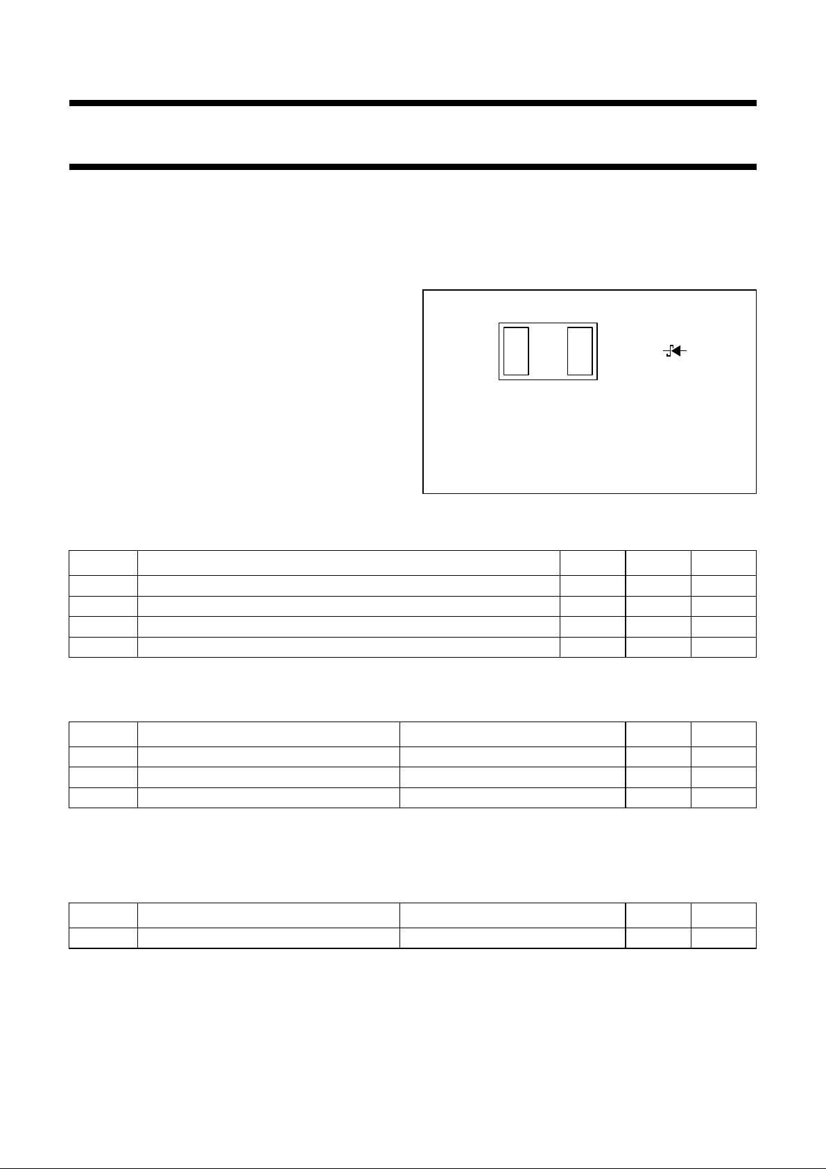
Bottom view
MDB391
• Ultra high-speed switching
• High frequency applications
Marking code: S1.
The marking bar indicates the cathode.
• Mobile communication,digital (still) cameras, PDAs and
PCMCIA cards.
Fig.1 Simplified outline (SOD882) and symbol.
LIMITING VALUES
In accordance with the Absolute Maximum Rating System (IEC 60134).
SYMBOL PARAMETER MIN. MAX. UNIT
V
R
I
F
T
stg
T
j
continuous reverse voltage − 40 V
continuous forward current − 20 mA
storage temperature −65 +150 °C
junction temperature − 150 °C
ELECTRICAL CHARACTERISTICS
T
=25°C unless otherwise specified.
amb
SYMBOL PARAMETER CONDITIONS MAX. UNIT
V
F
I
R
C
d
forward voltage IF= 2 mA; see Fig.2; note 1 800 mV
reverse current VR= 40 V; see Fig.3; note 1 1 µA
diode capacitance VR= 0 V; f = 1 MHz; see Fig.4 0.6 pF
Note
1. Pulse test: pulse width = 300 µs; δ = 0.02.
THERMAL CHARACTERISTICS
SYMBOL PARAMETER CONDITIONS VALUE UNIT
R
th j-a
thermal resistance from junction to ambient note 1 500 K/W
Note
1. Refer to SOD882 standard mounting conditions (footprint), FR4 with 60 µm copper strip line.
Soldering
Reflow soldering is the only recommended soldering method.
2003 May 15 2
Page 3

Philips Semiconductors Product specification
Schottky barrier diode 1PS10SB62
GRAPHICAL DATA
10
handbook, halfpage
I
F
(mA)
MDB388
0
(2)
(1)
−1
10
−2
10
(3)
VF (V)
(1) T
(2) T
(3) T
amb
amb
amb
= 125 °C.
=85°C.
=25°C.
Fig.2 Forward current as a function of forward
voltage; typical values.
4
10
handbook, halfpage
I
R
(nA)
3
10
2
10
(1)
(2)
MDB389
10
(3)
0
−1
2.00.0 0.4 0.8 1.2 1.6
10
(1) T
(2) T
(3) T
amb
amb
amb
= 125 °C.
=85°C.
=25°C.
VR (V)
401003020
Fig.3 Reverse current as a function of reverse
voltage; typical values.
0.4
handbook, halfpage
C
d
(pF)
MDB390
0.36
0.32
0.28
0.24
0.2
01020 40
f = 1 MHz; T
amb
=25°C.
30
VR (V)
Fig.4 Diode capacitance as a function of reverse
voltage; typical values.
2003 May 15 3
Page 4
Philips Semiconductors Product specification
Schottky barrier diode 1PS10SB62
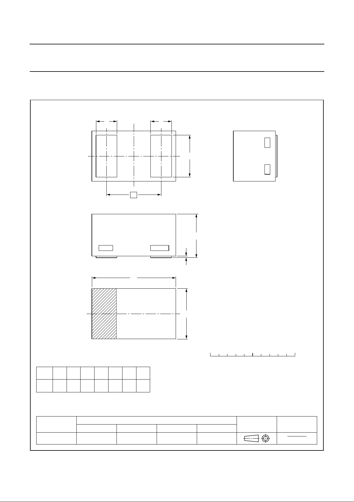
PACKAGE OUTLINE
Leadless ultra small plastic package; 2 terminals; body 1.0 x 0.6 x 0.5 mm SOD882
L
1
e
1
E
L
2
b
A
A
1
(2)
DIMENSIONS (mm are the original dimensions)
A
(1)
UNIT
A
0.50
mm
0.46
Notes
1. Including plating thickness
2. The marking bar indicates the cathode
OUTLINE
VERSION
SOD882
1
be
max.
0.03
DE
0.55
0.62
1.02
0.47
0.55
IEC JEDEC JEITA
0.95
0.65
L
1
0.30
0.22
REFERENCES
2003 May 15 4
D
0 0.5 1 mm
scale
EUROPEAN
PROJECTION
ISSUE DATE
03-04-16
03-04-17
Page 5

Philips Semiconductors Product specification
Schottky barrier diode 1PS10SB62
DATA SHEET STATUS
LEVEL
DATA SHEET
STATUS
(1)
PRODUCT
STATUS
(2)(3)
DEFINITION
I Objective data Development This data sheet contains data from the objective specification for product
development. Philips Semiconductors reserves the right to change the
specification in any manner without notice.
II Preliminary data Qualification This data sheet contains data from the preliminary specification.
Supplementary data will be published at a later date. Philips
Semiconductors reserves the right to change the specification without
notice, in order to improve the design and supply the best possible
product.
III Product data Production This data sheet contains data from the product specification. Philips
Semiconductors reserves the right to make changes at any time in order
to improve the design, manufacturing and supply. Relevant changes will
be communicated via a Customer Product/Process Change Notification
(CPCN).
Notes
1. Please consult the most recently issued data sheet before initiating or completing a design.
2. The product status of the device(s) described in this data sheet may have changed since this data sheet was
published. The latest information is available on the Internet at URL http://www.semiconductors.philips.com.
3. For datasheets describingmultiple type numbers,the highest-levelproduct status determinesthe datasheet status.
DEFINITIONS
DISCLAIMERS
Short-form specification The data in a short-form
specification is extracted from a full data sheet with the
same type number and title. For detailed information see
the relevant data sheet or data handbook.
Limiting valuesdefinition Limiting values givenare in
accordance with the Absolute Maximum Rating System
(IEC 60134). Stress above one or more of the limiting
values may cause permanent damage to the device.
These are stress ratings only and operation of the device
atthese orat any otherconditions abovethosegiven inthe
Characteristics sectionsof the specification isnot implied.
Exposure to limiting values for extended periods may
affect device reliability.
Application information Applications that are
described herein for any of these products are for
illustrative purposes only. Philips Semiconductors make
norepresentation orwarrantythat suchapplicationswill be
suitable for the specified use without further testing or
modification.
Life support applications These products are not
designed for use in life support appliances, devices, or
systems where malfunction of these products can
reasonably be expected to result in personal injury.Philips
Semiconductorscustomers usingorselling these products
for use in such applications do so at their own risk and
agree to fully indemnify Philips Semiconductors for any
damages resulting from such application.
Right to make changes Philips Semiconductors
reserves the right to make changes in the products including circuits, standard cells, and/or software described or contained herein in order to improve design
and/or performance. When theproduct isin fullproduction
(status ‘Production’), relevant changes will be
communicated via a Customer Product/Process Change
Notification (CPCN). Philips Semiconductors assumes no
responsibility or liability for the use of any of these
products, conveys no licence or title under any patent,
copyright, or mask work right to these products, and
makes no representations or warranties that these
products are free from patent, copyright, or mask work
right infringement, unless otherwise specified.
2003 May 15 5
Page 6

Philips Semiconductors Product specification
Schottky barrier diode 1PS10SB62
NOTES
2003 May 15 6
Page 7

Philips Semiconductors Product specification
Schottky barrier diode 1PS10SB62
NOTES
2003 May 15 7
Page 8

Philips Semiconductors – a w orldwide compan y
Contact information
For additional information please visit http://www.semiconductors.philips.com. Fax: +31 40 27 24825
For sales offices addresses send e-mail to: [email protected].
© Koninklijke Philips Electronics N.V. 2003
All rights are reserved. Reproduction in whole or in part is prohibited without the prior written consent of the copyright owner.
The information presented in thisdocument does not form partof any quotation or contract, is believed to be accurate and reliable and may be changed
without notice. No liability will be accepted by the publisher for any consequence of its use. Publication thereof does not convey nor imply any license
under patent- or other industrial or intellectual property rights.
Printed in The Netherlands 613514/01/pp8 Date of release: 2003 May15 Document order number: 9397 750 11303
SCA75
 Loading...