

Datasheet 1PMT5948BT3, 1PMT5947BT3, 1PMT5946BT3, 1PMT5945BT3, 1PMT5944BT3 Datasheet (Motorola)
...Page 1
1
MOTOROLA
1PMT5913BT3 through 1PMT5948BT3
%% $% &# "&!%
"! !# "$
"'# %
This complete new line of zener/tvs diodes offers a 2.5 watt series in a micro
miniature, space saving surface mount package. The Powermite zener/tvs
diodes are designed for use as a tvs or a regulation device in automotive and
telecommunication applications where efficiency, low leakage, size/height and
profile are important.
Features:
• Voltage Range – 3.3 to 91 V
• ESD Rating of Class 3 (> 16 kV) per Human Body Model
• Low Profile – maximum height of 1.1mm
• Integral Heat Sink/Locking Tabs
• Full metallic bottom eliminates flux entrapment
• Small Footprint – Footprint area of 8.45mm
2
• Supplied in 12mm tape and reel – 12,000 units per reel
• Powermite is JEDEC Registered as DO–216AA
MAXIMUM RATINGS
Rating Symbol Value Unit
DC Power Dissipation @ TL = 75°C, Measured at Zero Lead Length
Derate above 75°C
°PD° 2.5
40
°Watts°
mW/°C
DC Power Dissipation @ TA = 25°C(1)
Derate above 25°C
°PD° 380
2.8
°mW
mW/°C
Thermal Resistance from Junction to Lead R
θJL
26 °C/W
Thermal Resistance from Junction to Ambient R
θJA
324 °C/W
Operating and Storage Junction Temperature Range TJ, T
stg
– 65 to +150 °C
Typical Ppk Dissipation @ TL < 25°C, (PW–10/1000 µs per Figure 8)
(2)
P
pk
200 Watts
Typical Ppk Dissipation @ TL < 25°C, (PW–8/20 µs per Figure 9)
(2)
P
pk
1000 Watts
(1)FR4 Board, within 1” to device, using Motorola minimum recommended footprint, as shown in case 403A outline dimensions spec.
(2)Non–repetitive current pulse.
This document contains preview information only and is subject to change without notice.
Powermite is a registered trademark of Microsemi Corporation.
Thermal Clad is a trademark of the Bergquist Company.
SEMICONDUCTOR TECHNICAL DATA
Order this document
by 1PMT5913BT3/D
Motorola, Inc. 1996
%#"&
PLASTIC SURFACE MOUNT
ZENER DIODES
2.5 WATTS
3.3–91 VOLTS
CASE 457–01
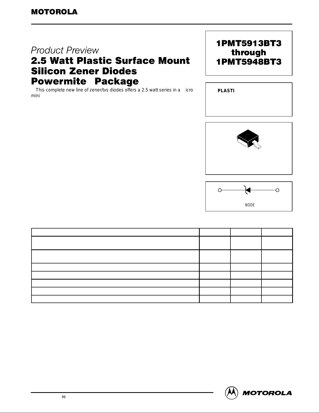
PLASTIC
1
2
1 2
1: CATHODE
2: ANODE
Page 2

MOTOROLA
2
1PMT5913BT3 through 1PMT5948BT3
ELECTRICAL CHARACTERISTICS
(VF = 1.5 Volts Max @ IF = 200 mAdc for all types.)
Nominal
Zener Voltage
Test
Max Zener Impedance (Note 2)
Max Reverse
Leakage Current
Maximum DC
Zener
Device
*
VZ @ I
ZT
Volts
(Note 1)
Current
I
ZT
mA
Z
ZT
@ I
ZT
Ohms
Z
ZK
Ohms
I
ZK
mA
@
I
R
µA
V
R
Volts
@
Current
I
ZM
mAdc
Device
Marking
1PMT5913BT3 3.3 113.6 10 500 1 100 1 454 913B
1PMT5914BT3 3.6 104.2 9 500 1 75 1 416 914B
1PMT5915BT3 3.9 96.1 7.5 500 1 25 1 384 915B
1PMT5916BT3 4.3 87.2 6 500 1 5 1 348 916B
1PMT5917BT3 4.7 79.8 5 500 1 5 1.5 319 917B
1PMT5918BT3 5.1 73.5 4 350 1 5 2 294 918B
1PMT5919BT3 5.6 66.9 2 250 1 5 3 267 919B
1PMT5920BT3 6.2 60.5 2 200 1 5 4 241 920B
1PMT5921BT3 6.8 55.1 2.5 200 1 5 5.2 220 921B
1PMT5922BT3 7.5 50 3 400 0.5 5 6.8 200 922B
1PMT5923BT3 8.2 45.7 3.5 400 0.5 5 6.5 182 923B
1PMT5924BT3 9.1 41.2 4 500 0.5 5 7 164 924B
1PMT5925BT3 10 37.5 4.5 500 0.25 5 8 150 925B
1PMT5926BT3 11 34.1 5.5 550 0.25 1 8.4 136 926B
1PMT5927BT3 12 31.2 6.5 550 0.25 1 9.1 125 927B
1PMT5928BT3 13 28.8 7 550 0.25 1 9.9 115 928B
1PMT5929BT3 15 25 9 600 0.25 1 11.4 100 929B
1PMT5930BT3 16 23.4 10 600 0.25 1 12.2 93 930B
1PMT5931BT3 18 20.8 12 650 0.25 1 13.7 83 931B
1PMT5932BT3 20 18.7 14 650 0.25 1 15.2 75 932B
1PMT5933BT3 22 17 17.5 650 0.25 1 16.7 68 933B
1PMT5934BT3 24 15.6 19 700 0.25 1 18.2 62 934B
1PMT5935BT3 27 13.9 23 700 0.25 1 20.6 55 935B
1PMT5936BT3 30 12.5 26 750 0.25 1 22.8 50 936B
1PMT5937BT3 33 11.4 33 800 0.25 1 25.1 45 937B
1PMT5938BT3 36 10.4 38 850 0.25 1 27.4 41 938B
1PMT5939BT3 39 9.6 45 900 0.25 1 29.7 38 939B
1PMT5940BT3 43 8.7 53 950 0.25 1 32.7 34 940B
1PMT5941BT3 47 8 67 1000 0.25 1 35.8 31 941B
1PMT5942BT3 51 7.3 70 1100 0.25 1 38.8 29 942B
1PMT5943BT3 56 6.7 86 1300 0.25 1 42.6 26 943B
1PMT5944BT3 62 6 100 1500 0.25 1 47.1 24 944B
1PMT5945BT3 68 5.5 120 1700 0.25 1 51.7 22 945B
1PMT5946BT3 75 5 140 2000 0.25 1 56 20 946B
1PMT5947BT3 82 4.6 160 2500 0.25 1 62.2 18 947B
1PMT5948BT3 91 4.1 200 3000 0.25 1 69.2 16 948B
* TOLERANCE AND VOLTAGE DESIGNATION Tolerance designation — The type numbers listed indicate a tolerance of ±5%.
Devices listed in bold, italic are Motorola preferred devices.
Page 3

3
MOTOROLA
1PMT5913BT3 through 1PMT5948BT3
TYPICAL CHARACTERISTICS
Figure 1. Steady State Power Derating Figure 2. Maximum Surge Power
Figure 3. Maximum Surge Power Figure 4. Pulse Waveform 10/1000
Figure 5. Zener Voltage – To 12 Volts Figure 6. Zener Voltage – 14 To 200 Volts
0 25 50 75 100 125 150
6
5
4
3
2
0
T, TEMPERATURE (°C)
P , MAXIMUM POWER DISSIPATION (WATTS)
D
10
100
1000
0.1 1 10 100
PW, PULSE WIDTH (ms)
P , PEAK SURGE POWER (WATTS)
PK
RECTANGULAR
NONREPETITIVE
WAVEFORM
1
T
L
T
A
10
1
0.1 1 100.01
Tp, PULSE WIDTH (ms)
P , PEAK POWER (kW)
PK
NONREPETITIVE
EXPONENTIAL
PULSE WAVEFORM
TJ = 25
°
C
2 4 6 8 10 12
10
8
6
4
2
0
–2
–4
VZ, ZENER VOLTAGE (VOLTS)
, TEMPERATURE COEFFICIENT (mV/ C)
°θ
VZ
VZ @ I
ZT
200
100
70
50
30
20
10
10 20 30 50 70 100 200
VZ, ZENER VOLTAGE (VOLTS)
, TEMPERATURE COEFFICIENT (mV/ C)
°
θ
VZ
VZ @ I
ZT
120
100
80
60
40
0
0 1 2 3 4
t, TIME (ms)
I
ppm
, PEAK PULSE CURRENT (%)
20
5
TA = 25°C
PW (ID) IS DEFINED AS THE
POINT WHERE THE PEAK CURRENT
DECAYS TO 50% OF Ipp.
= 10 µs
PEAK VALUE
I
ppm
HALF VALUE – Ipp/2
10/1000 µs WAVEFORM
AS DEFINED BY R.E.A.
t
d
NOTE 1. ZENER VOLTAGE (VZ) MEASUREMENT
Nominal zener voltage is measured with the device junction
in thermal equilibrium with ambient temperature at 25°C
0.1
0.001
Page 4

MOTOROLA
4
1PMT5913BT3 through 1PMT5948BT3
Figure 7. VZ = 3.3 thru 10 Volts Figure 8. VZ = 12 thru 82 Volts
Z
(ac) = 0.1 IZ(dc) with the ac frequency = 60 Hz.
Figure 9. Effect of Zener Voltage Figure 10. Effect of Zener Current
IZ, ZENER TEST CURRENT (mA)
1k
500
200
100
50
20
10
5
2
1
0.5 1 2 5 10 20 50 100 200 500
Z , DYNAMIC IMPEDANCE (OHMS)
Z
TJ = 25°C
i
Z(rms)
= 0.1 I
Z(dc)
VZ =150V
91V
62V
22V
12V
6.8V
VZ, ZENER VOLTAGE (VOLTS)
5 7 10 20 30 50 70 100
200
100
70
50
30
20
10
7
5
3
2
Z , DYNAMIC IMPEDANCE (OHMS)
Z
10mA
I
Z(dc)
= 1mA
20mA
i
Z(rms)
= 0.1 I
Z(dc)
0 1 2 3 4 5 6 7 8 9 10
100
50
30
20
10
1
0.5
0.3
0.2
0.1
VZ, ZENER VOLTAGE (VOLTS)
I , ZENER CURRENT (mA)
Z
2
5
3
0 10 20 30 40 50 60 70 80 90 100
VZ, ZENER VOLTAGE (VOLTS)
I , ZENER CURRENT (mA)
Z
100
50
30
20
10
1
0.5
0.3
0.2
0.1
2
5
3
NOTE 2. ZENER IMPEDANCE (ZZ) DERIVATION
ZZT and ZZK are measured by dividing the ac voltage drop
across the device by the ac current applied. The specified
limits are for I
Page 5

5
MOTOROLA
1PMT5913BT3 through 1PMT5948BT3
INFORMATION FOR USING THE POWERMITE SURFACE MOUNT PACKAGE
MINIMUM RECOMMENDED FOOTPRINT FOR SURFACE MOUNTED APPLICATIONS
Surface mount board layout is a critical portion of the total
design. The footprint for the semiconductor packages must
be the correct size t o insure proper s older connection
interface between the board and the package. With the
correct pad g eometry, the packages will self align when
subjected to a solder reflow process.
POWERMITE
0.100
2.54
0.025
0.635
0.050
1.27
0.105
2.67
0.030
0.762
inches
mm
POWERMITE POWER DISSIPATION
The power dissipation of the Powermite is a function of the
drain pad size. This can vary from the minimum pad size for
soldering to a pad size given for maximum power dissipation.
Power dissipation for a surface mount device is determined
by T
J(max)
, the maximum rated junction temperature of the
die, R
θJA
, the thermal resistance from the device junction to
ambient, and the operating temperature, TA. Using the
values provided o n the data s heet f or the P owermite
package, PD can be calculated as follows:
The values for the equation are found in the maximum
ratings table on the data sheet. Substituting these values into
the equation for an ambient temperature TA of 25°C, one can
calculate the power dissipation of the device which in this
case is 386 milliwatts.
The 324°C/W for the Powermite package assumes the use
of the recommended footprint on a glass epoxy printed circuit
board to achieve a power dissipation of 386 milliwatts. There
are other alternatives to achieving higher power dissipation
from the Powermite package. Another alternative would be
to use a ceramic substrate or an aluminum core board such
as Thermal Clad. Using a board material such as Thermal
Clad, an aluminum core board, the power dissipation can be
doubled using the same footprint.
SOLDERING PRECAUTIONS
The melting temperature of solder is higher than the rated
temperature of the device. When the entire device is heated
to a high temperature, failure to complete soldering within a
short time could result in device failure. Therefore, the
following items should always be observed in order to
minimize the thermal stress to which the devices are
subjected.
• Always preheat the device.
• The delta temperature between the preheat and soldering
should be 100°C or less.*
• When preheating and soldering, the temperature of the
leads and the case must not exceed the maximum
temperature ratings as shown on the data sheet. When
using infrared heating with the reflow soldering method,
the difference shall be a maximum of 10°C.
• The soldering temperature and time shall not exceed
260°C for more than 10 seconds.
• When shifting from preheating to soldering, the maximum
temperature gradient shall be 5°C or less.
• After soldering has been completed, the device should be
allowed to cool naturally for at least three minutes.
Gradual cooling should be used as the use of forced
cooling will increase the temperature gradient and result
in latent failure due to mechanical stress.
• Mechanical stress or shock should not be applied during
cooling.
* Soldering a device without preheating can cause excessive
thermal shock and stress which can result in damage to the
device.
PD =
PD =
T
150°C – 25°C
324°C/W
J(max)
R
θJA
– T
A
= 386 milliwatts
Page 6

MOTOROLA
6
1PMT5913BT3 through 1PMT5948BT3
OUTLINE DIMENSIONS
CASE 457–01
ISSUE O
DIM MIN MAX MIN MAX
INCHESMILLIMETERS
A 1.75 2.15 0.069 0.081
B 1.75 2.15 0.069 0.086
C 0.85 1.15 0.033 0.045
D 0.40 0.65 0.016 0.026
F 0.70 1.00 0.028 0.039
H –0.05 +0.10 –0.002 +0.004
J 0.10 0.25 0.004 0.010
K 3.60 4.15 0.142 0.163
L 0.50 0.80 0.020 0.031
R 1.20 1.50 0.047 0.059
S 0.50 REF 0.020
NOTES:
1. DIMENSIONING AND TOLERANCING PER ANSI
Y14.5M, 1982.
2. CONTROLLING DIMENSION: MILLIMETER.
3. DIMENSION A DOES NOT INCLUDE MOLD FLASH,
PROTRUSIONS OR GATE BURRS. MOLD FLASH,
PROTRUSIONS OR GATE BURRS SHALL NOT
EXCEED 0.15 (0.006) PER SIDE.
S
B
M
0.08 (0.003) C
S
T
–A–
–B–
S
J
K
–T–
H
L
J
C
D
S
B
M
0.08 (0.003) C
S
T
F
TERM. 1 CATHODE
TERM. 2 ANODE
R
Motorola reserves the right to make changes without further notice to any products herein. Motorola makes no warranty , representation or guarantee regarding
the suitability of its products for any particular purpose, nor does Motorola assume any liability arising out of the application or use of any product or circuit, and
specifically disclaims any and all liability , including without limitation consequential or incidental damages. “Typical” parameters which may be provided in Motorola
data sheets and/or specifications can and do vary in different applications and actual performance may vary over time. All operating parameters, including “Typicals”
must be validated for each customer application by customer’s technical experts. Motorola does not convey any license under its patent rights nor the rights of
others. Motorola products are not designed, intended, or authorized for use as components in systems intended for surgical implant into the body, or other
applications intended to support or sustain life, or for any other application in which the failure of the Motorola product could create a situation where personal injury
or death may occur. Should Buyer purchase or use Motorola products for any such unintended or unauthorized application, Buyer shall indemnify and hold Motorola
and its officers, employees, subsidiaries, affiliates, and distributors harmless against all claims, costs, damages, and expenses, and reasonable attorney fees
arising out of, directly or indirectly, any claim of personal injury or death associated with such unintended or unauthorized use, even if such claim alleges that
Motorola was negligent regarding the design or manufacture of the part. Motorola and are registered trademarks of Motorola, Inc. Motorola, Inc. is an Equal
Opportunity/Affirmative Action Employer.
How to reach us:
USA/EUROPE/Locations Not Listed: Motorola Literature Distribution; JAPAN: Nippon Motorola Ltd.; Tatsumi–SPD–JLDC, 6F Seibu–Butsuryu–Center,
P.O. Box 20912; Phoenix, Arizona 85036. 1–800–441–2447 or 602–303–5454 3–14–2 Tatsumi Koto–Ku, Tokyo 135, Japan. 03–81–3521–8315
MFAX: RMFAX0@email.sps.mot.com – TOUCHTONE 602–244–6609 ASIA/PACIFIC: Motorola Semiconductors H.K. Ltd.; 8B Tai Ping Industrial Park,
INTERNET: http://Design–NET.com 51 Ting Kok Road, Tai Po, N.T., Hong Kong. 852–26629298
1PMT5913BT3/D
*1PMT5913BT3/D*
◊
 Loading...