

Page 1
®
1N 6263
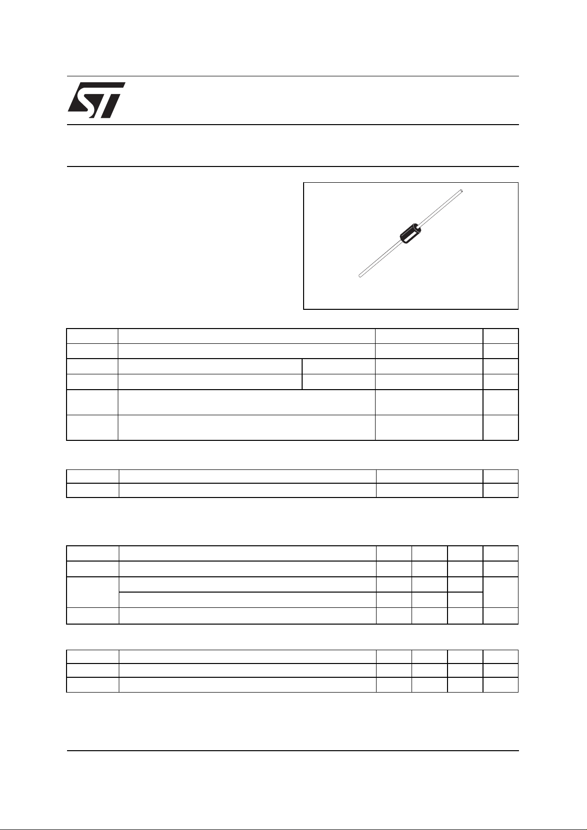
SMALL SIGNAL SCHOTTKY DIODE
DESCRIPTION
Metal to silicon junction diode featuring high breakdown, low turn-on voltage and ultrafast switching.
Primarly intended for high lev el UHF/VHF detection
and pulse application with broad dynamic range.
ABSOLUTE RAT INGS (limiting values)
Symbol Parameter Value Unit
V
I
FSM
T
RRM
I
F
stg
T
T
L
Repetitive Peak Reverse Voltage 60 V
Forward Continuous Current*
Surge non Repetitive Forward Current*
T
t
p
= 25
a
≤ 1s
C
°
Storage and Junction Temperature Range - 65 to 200
j
Maximum Lead Temperature for Soldering during 10s at 4mm
from Case
DO 35
(Glass)
15 mA
50 mA
- 65 to 200
230
C
°
C
°
THERMAL RESISTANCE
Symbol Test Conditions Value Unit
R
th(j-a)
Junction-ambient* 400
ELECTRICAL CHARACTERISTICS
STATIC CHARACTERISTICS
Symbol Test Conditions Min. Typ. Max. Unit
V
BR
* *
V
F
I
* *
R
T
= 25°CI
amb
= 25°CI
T
amb
T
= 25°CI
amb
= 25°CV
T
amb
= 10µA
R
= 1mA
F
= 15mA
F
= 50V
R
60 V
0.41 V
1
0.2
DYNAMIC CHARACTERISTICS
Symbol Test Conditions Min. Typ. Max. Unit
C
τ
* On infinite heatsink with 4mm lead length
** Pulse test: t
Matched batches available on request. Test conditions (forward voltage and/or capacitance) according to customer specification.
= 25°CV
T
amb
T
= 25°CI
amb
300µs δ < 2%
≤
p
.
= 0V f = 1MHz
R
= 5mA Krakauer Method
F
August 1999 Ed: 1A
2.2 pF
100 ps
C/W
°
µ
A
1/3
Page 2
1N 6263
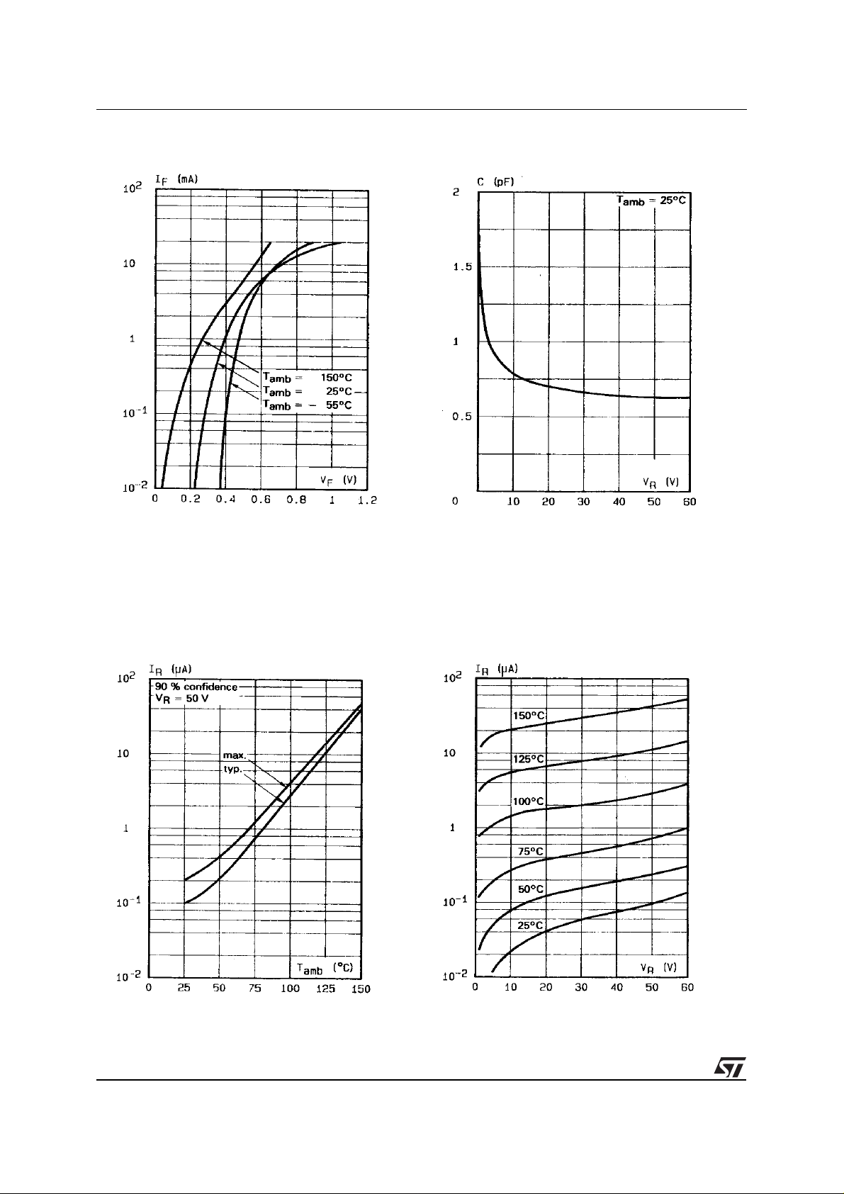
Fig.1 :
Forward current versus forward voltage
(typical values).
Fig.2 :
Capacitance C versus reverse applied
voltage V
(typical values).
R
Fig.3 :
Reverse current versus ambient
temperature.
Fig.4 :
Reverse current versus continuous
reverse voltage (typical values).
2/3
Page 3

PACKAGE MECHANICAL DATA
DO 35 Glass
CA
O
/
O
/
D
Cooling method : by convection and conduction
Marking: clear, ring at cathode end.
Weight: 0.15g
D
C
/
BO
DIMENSIONS
REF.
Millimeters Inches
Min. Max. Min. Max.
A 3.05 4.50 0.120 0.177
B 1.53 2.00 0.060 0.079
C 12.7 0.500
D 0.458 0.558 0.018 0.022
1N 6263
Information furnished is believed to be accurate and reliable. Howev er, STMicroelectronics assumes no responsibility for the consequences of
use of such information nor for any infringement of patents or other rights of third parties which may result from its us e. No license is granted
by implication or otherwise under any patent or patent rights of STMicroelectronics. Specifications mentioned in this publication are subjec t to
change without notice. This publication supersedes and replaces all information previously supplied.
STMicroelectronics products are not authorized for use as critical components in life support devices or systems without express written approval
of STMicroelectronic s.
The ST logo is a registered trademark of STMicroelectronics
© 1999 STMicroelectronics - Printed in Italy - All rights reserved.
STMicroelectronics GROUP OF COMPANIES
Australia - Brazil - China - Finland - France - Germany - Hong Kong - India - Italy - Japan - Malaysia
Malta - Morocco - Singapore - Spain - Sweden - Switzerland - United Kingdom - U.S.A.
http://www.st.com
3/3
 Loading...