

Page 1

1N5820, 1N5821, 1N5822
1N5820 and 1N5822 are Preferred Devices
Axial Lead Rectifiers
. . . employing the Schottky Barrier principle in a large area
metal–to–silicon power diode. State–of–the–art geometry features
chrome barrier metal, epitaxial construction with oxide passivation
and metal overlap contact. Ideally suited for use as rectifiers in
low–voltage, high–frequency inverters, free wheeling diodes, and
polarity protection diodes.
• Extremely Low V
• Low Power Loss/High Efficiency
• Low Stored Charge, Majority Carrier Conduction
Mechanical Characteristics:
• Case: Epoxy, Molded
• Weight: 1.1 gram (approximately)
• Finish: All External Surfaces Corrosion Resistant and Terminal
Leads are Readily Solderable
• Lead and Mounting Surface Temperature for Soldering Purposes:
220°C Max. for 10 Seconds, 1/16″ from case
• Shipped in plastic bags, 500 per bag
• Available Tape and Reeled, 1500 per reel, by adding a “RL’’ suffix to
the part number
• Polarity: Cathode indicated by Polarity Band
• Marking: 1N5820, 1N5821, 1N5822
MAXIMUM RATINGS
Please See the Table on the Following Page
F
http://onsemi.com
SCHOTTKY BARRIER
RECTIFIERS
3.0 AMPERES
20, 30, 40 VOLTS
AXIAL LEAD
CASE 267–03
STYLE 1
MARKING DIAGRAM
Semiconductor Components Industries, LLC, 2000
October, 2000 – Rev. 3
1N582x
1N582x = Device Code
x = 0, 1 or 2
ORDERING INFORMATION
Device Package Shipping
1N5820 Axial Lead 500 Units/Bag
1N5820RL Axial Lead 1500/Tape & Reel
1N5821 Axial Lead 500 Units/Bag
1N5821RL Axial Lead 1500/Tape & Reel
1N5822 Axial Lead 500 Units/Bag
1N5822RL Axial Lead 1500/Tape & Reel
Preferred devices are recommended choices for future use
and best overall value.
1 Publication Order Number:
1N5820/D
Page 2

1N5820, 1N5821, 1N5822
MAXIMUM RATINGS
Rating Symbol 1N5820 1N5821 1N5822 Unit
Peak Repetitive Reverse Voltage
Working Peak Reverse Voltage
DC Blocking Voltage
Non–Repetitive Peak Reverse Voltage V
RMS Reverse Voltage V
Average Rectified Forward Current (Note 1.)
V
0.2 V
R(equiv)
= 28°C/W, P.C. Board Mounting, see Note 5.)
(R
θ
JA
R(dc)
, TL = 95°C
Ambient Temperature
Rated V
R
θ
JA
, P
R(dc)
= 28°C/W
F(AV)
= 0
Non–Repetitive Peak Surge Current
(Surge applied at rated load conditions, half wave, single phase
60 Hz, T
= 75°C)
L
Operating and Storage Junction Temperature Range
(Reverse Voltage applied)
Peak Operating Junction Temperature (Forward Current applied) T
*THERMAL CHARACTERISTICS (Note 5.)
Characteristic
Thermal Resistance, Junction to Ambient R
*ELECTRICAL CHARACTERISTICS (T
Characteristic
Maximum Instantaneous Forward Voltage (Note 2.)
(i
= 1.0 Amp)
F
= 3.0 Amp)
(i
F
(i
= 9.4 Amp)
F
Maximum Instantaneous Reverse Current
@ Rated dc Voltage (Note 2.)
= 25°C
T
L
T
= 100°C
L
1. Lead Temperature reference is cathode lead 1/32″ from case.
2. Pulse Test: Pulse Width = 300 µs, Duty Cycle =2.0%.
*Indicates JEDEC Registered Data for 1N5820–22.
= 25°C unless otherwise noted) (Note 1.)
L
V
RRM
V
RWM
V
RSM
R(RMS)
I
O
T
I
FSM
TJ, T
J(pk)
R
A
stg
20 30 40 V
24 36 48 V
14 21 28 V
90 85 80 °C
80 (for one cycle) A
Symbol 1N5820 1N5821 1N5822 Unit
V
F
0.370
0.475
0.850
i
R
2.0
20
3.0
65 to +125 °C
150
°C
Symbol Max Unit
θ
JA
0.380
0.500
0.900
28 °C/W
0.390
0.525
0.950
mA
2.0
20
2.0
20
A
V
http://onsemi.com
2
Page 3

1N5820, 1N5821, 1N5822
NOTE 3. — DETERMINING MAXIMUM RATINGS
Reverse power dissipation and the possibility of thermal
runaway must be considered when operating this rectifier at
reverse voltages above 0.1 V
. Proper derating may be
RWM
accomplished by use of equation (1).
T
where T
= T
A(max)
= Maximum allowable ambient temperature
A(max)
T
= Maximum allowable junction temperature
J(max)
J(max)
R
P
R
F(AV)
JA
θ
P
(1)
R(AV)
JA
θ
(125°C or the temperature at which thermal
runaway occurs, whichever is lowest)
P
= Average forward power dissipation
F(AV)
P
= Average reverse power dissipation
R(AV)
R
= Junction–to–ambient thermal resistance
JA
θ
Figures 1, 2, and 3 permit easier use of equation (1) by
taking reverse power dissipation and thermal runaway into
consideration. The figures solve for a reference temperature
as determined by equation (2).
TR = T
J(max)
R
P
JA
R(AV)
θ
(2)
Substituting equation (2) into equation (1) yields:
T
Inspection of equations (2) and (3) reveals that T
A(max)
= TR R
P
JA
F(AV)
θ
is the
R
(3)
ambient temperature at which thermal runaway occurs or
where TJ = 125°C, when forward power is zero. The
transition from one boundary condition to the other is
evident on the curves of Figures 1, 2, and 3 as a difference
in the rate of change of the slope in the vicinity of 115°C. The
data of Figures 1, 2, and 3 is based upon dc conditions. For
use in common rectifier circuits, Table 1. indicates
suggested factors for an equivalent dc voltage to use for
conservative design, that is:
V
R(equiv)
= V
F (4)
(FM)
The factor F is derived by considering the properties of the
various rectifier circuits and the reverse characteristics of
Schottky diodes.
EXAMPLE: Find T
for 1N5821 operated in a
A(max)
12–volt dc supply using a bridge circuit with capacitive filter
such that I
Voltage = 10 V
Step 1. Find V
= 2.0 A (I
DC
, R
(rms)
R(equiv).
V
= 1.0 A), I
F(AV)
= 40°C/W.
JA
θ
Read F = 0.65 from Table 1. ,
= (1.41) (10) (0.65) = 9.2 V.
R(equiv)
(FM)/I(AV)
= 10, Input
Step 2. Find TR from Figure 2. Read TR = 108°C
Step 3. Find P
F(AV)
@
Step 4. Find T
@ VR = 9.2 V and R
from Figure 6. **Read P
I
(FM)
I
(AV)
A(max)
T
A(max)
10 and I
from equation (3).
= 108 (0.85) (40) = 74°C.
F(AV)
= 40°C/W.
JA
θ
1.0 A.
F(AV)
= 0.8 5 W
**Values given are for the 1N5821. Power is slightly lower
for the 1N5820 because of its lower forward voltage, and
higher for the 1N5822. Variations will be similar for the
MBR–prefix devices, using P
from Figure 6.
F(AV)
Table 1. Values for Factor F
Full Wave,
Circuit Half Wave Full Wave, Bridge
Load Resistive Capacitive* Resistive Capacitive Resistive Capacitive
Sine Wave 0.5 1.3 0.5 0.65 1.0 1.3
Square Wave 0.75 1.5 0.75 0.75 1.5 1.5
*Note that V
R(PK)
2.0 V
. †Use line to center tap voltage for Vin.
in(PK)
Center Tapped*†
http://onsemi.com
3
Page 4
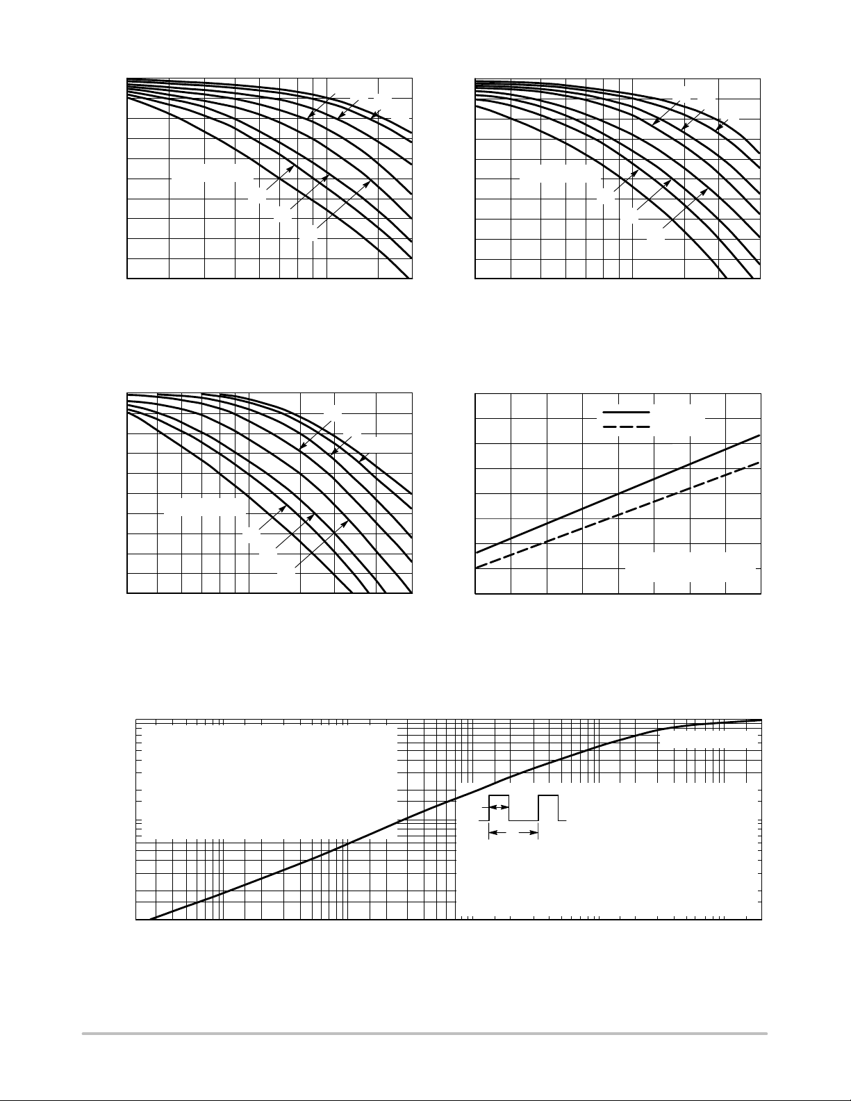
1N5820, 1N5821, 1N5822
125
°
115
105
95
85
, REFERENCE TEMPERATURE ( C)T
R
T
75
125
°
115
105
95
85
, REFERENCE TEMPERATURE ( C)
R
75
20
15
10
8.0
125
20
°
115
15
10
105
R
(°C/W) = 70
JA
50
40
28
5.03.0 4.0 7.0 10 20
, REVERSE VOLTAGE (VOLTS)
V
R
152.0
Figure 1. Maximum Reference T emperature
1N5820
95
85
, REFERENCE TEMPERATURE ( C)
R
T
75
R
(°C/W) = 70
JA
50
40
28
5.03.0 4.0 7.0 10 20
V
, REVERSE VOLTAGE (VOLTS)
R
15
Figure 2. Maximum Reference T emperature
1N5821
40
20
15
10
8.0
35
30
25
MAXIMUM
TYPICAL
20
R
(°C/W) = 70
JA
15
50
40
28
5.0 7.0 10 15 20 3/8 4/8 5/8 6/8 7/8 1.0
V
, REVERSE VOLTAGE (VOLTS)
R
304.0
, THERMAL RESISTANCE
JL
R
10
JUNCTION-TO-LEAD ( C/W)°
5.0
0
2/840
1/80
BOTH LEADS TO HEAT SINK,
EQUAL LENGTH
L, LEAD LENGTH (INCHES)
8.0
30
Figure 3. Maximum Reference T emperature
Figure 4. Steady–State Thermal Resistance
1N5822
1.0
The temperature of the lead should be measured using a ther
mocouple placed on the lead as close as possible to the tie point.
0.5
The thermal mass connected to the tie point is normally large
0.3
enough so that it will not significantly respond to heat surges
generated in the diode as a result of pulsed operation once
0.2
0.1
(NORMALIZED)
0.05
0.03
0.02
r(t), TRANSIENT THERMAL RESISTANCE
0.01
steady-state conditions are achieved. Using the measured val
ue of T
, the junction temperature may be determined by:
L
T
= TL + T
J
JL
t
∆T
∆T
r(t) = normalized value of transient thermal resistance at time, t, i.e.:
r(t
1
t
+ tp, etc.
1
P
p
JL
JL
pk
t
1
= P
• R
pk
= the increase in junction temperature above the lead temperature.
P
[D + (1 - D) • r(t
θ
JL
pk
DUTY CYCLE = t
PEAK POWER, Ppk, is peak of an
TIME
equivalent square power pulse.
+ tp) + r(tp) - r(t1)] where:
1
+ tp) = normalized value of transient thermal resistance at time
0.2 0.5 1.0 2.0 5.0 10 20 50 100 200 500 1.0 k 2.0 k 5.0 k 10 k
t, TIME (ms)
Figure 5. Thermal Response
http://onsemi.com
4
LEAD LENGTH = 1/4″
p/t1
20 k
Page 5

1N5820, 1N5821, 1N5822
10
7.0
5.0
3.0
2.0
1.0
0.7
0.5
SINE WAVE
I
(FM)
(ResistiveLoad)
I
(AV)
Capacitive
Loads
5.0
10
20
SQUARE WAVE
0.3
T
≈ 125°C
, AVERAGE POWER DISSIPATION (WATTS)
F(AV)
P
0.2
0.1
0.2 0.3 0.5 2.0
I
, AVERAGE FORWARD CURRENT (AMP)
F(AV)
0.7 1.0 7.0 10
J
3.00.1
5.0
Figure 6. Forward Power Dissipation 1N5820–22
NOTE 4. – APPROXIMATE THERMAL CIRCUIT MODEL
R
θ
T
dc
A(A)
S(A)
R
θ
T
L(A)
L(A)
R
θ
T
C(A)TJ
J(A)
R
θ
P
D
J(K)
R
θ
T
C(K)
L(K)
R
θ
S(K)
T
A(K)
T
L(K)
Use of the above model permits junction to lead thermal
resistance for any mounting configuration to be found. For
a given total lead length, lowest values occur when one side
of the rectifier is brought as close as possible to the heat sink.
Terms in the model signify:
T
= Ambient Temperature TC = Case Temperature
A
TL = Lead Temperature TJ = Junction Temperature
R
= Thermal Resistance, Heat Sink to Ambient
S
θ
R
= Thermal Resistance, Lead to Heat Sink
L
θ
R
= Thermal Resistance, Junction to Case
J
θ
PD = Total Power Dissipation = PF + P
R
PF = Forward Power Dissipation
PR = Reverse Power Dissipation
(Subscripts (A) and (K) refer to anode and cathode sides,
respectively.) Values for thermal resistance components
are:
R
= 42°C/W/in typically and 48°C/W/in maximum
L
θ
R
= 10°C/W typically and 16°C/W maximum
J
θ
The maximum lead temperature may be found as follows:
TL = T
where
T
J(max)
TJL R
JL
· P
JL
D
θ
NOTE 5. — MOUNTING DATA
Data shown for thermal resistance junction–to–ambient (R
for the mountings shown is to be used as typical guideline values
for preliminary engineering, or in case the tie point temperature
cannot be measured.
TYPICAL VALUES FOR R
Mounting
Method
1
2
3
Lead Length, L (in)
1/8 1/4 1/2 3/4
50 51 53 55 °C/W
58 59 61 63
θ
28
IN STILL AIR
JA
R
θ
°C/W
°C/W
JA
θ
JA
Mounting Method 1
P.C. Board where available
copper surface is small.
)
Mounting Method 2
LL
VECTOR PUSH-IN
TERMINALS T-28
LL
Mounting Method 3
P.C. Board with
2–1/2″ x 2–1/2″
copper surface.
L = 1/2″
BOARD GROUND
PLANE
http://onsemi.com
5
Page 6

1N5820, 1N5821, 1N5822
50
30
20
10
7.0
5.0
3.0
2.0
1.0
0.7
0.5
, INSTANTANEOUS FORWARD CURRENT (AMP)
F
i
0.3
0.2
0.1
T
= 100°C
J
25°C
100
70
50
30
20
, PEAK HALF-WAVE CURRENT (AMP)
FSM
I
10
100
50
20
10
5.0
2.0
1.0
0.5
T
= 75°C
L
f = 60 Hz
1 CYCLE
SURGE APPLIED AT RATED LOAD CONDITIONS
7.0 102.0 3.0
5.0 1001.0
NUMBER OF CYCLES
20 30 50 70
Figure 8. Maximum Non–Repetitive Surge
Current
T
= 125°C
J
100°C
75°C
0.07
0.05
500
300
200
C, CAPACITANCE (pF)
100
70
1.0
1.2
0.40 0.2 0.6 0.8
v
, INSTANTANEOUS FORWARD VOLTAGE (VOLTS)
F
1.10.30.1 0.5 0.7 1.30.9
Figure 7. Typical Forward Voltage
1N5820
T
= 25°C
J
f = 1.0 MHz
1N5822
0.7 7.0 20 30
1.00.5
2.0 3.0 5.0 10
VR, REVERSE VOLTAGE (VOLTS)
Figure 10. Typical Capacitance
1N5821
0.2
R
I , REVERSE CURRENT (mA)
1.4
0.1
0.05
0.02
0.01
25°C
4.0 12 20 28 36
8.00
16
, REVERSE VOLTAGE (VOLTS)
V
R
24 32 40
Figure 9. Typical Reverse Current
NOTE 6. — HIGH FREQUENCY OPERATION
Since current flow in a Schottky rectifier is the result of
majority carrier conduction, it is not subject to junction
diode forward and reverse recovery transients due to minority carrier injection and stored charge. Satisfactory circuit
analysis work may be performed by using a model consisting of an ideal diode in parallel with a variable capacitance.
(See Figure 10.)
1N5820
1N5821
1N5822
http://onsemi.com
6
Page 7

1N5820, 1N5821, 1N5822
PACKAGE DIMENSIONS
AXIAL LEAD
CASE 267–03
ISSUE G
NOTES:
D
1
B
K
A
2
K
1. DIMENSIONING AND TOLERANCING PER ANSI
Y14.5M, 1982.
2. CONTROLLING DIMENSION: INCH.
DIM MIN MAX MIN MAX
A 0.370 0.380 9.40 9.65
B 0.190 0.210 4.83 5.33
D 0.048 0.052 1.22 1.32
K 1.000 --- 25.40 ---
STYLE 1:
PIN 1. CATHODE (POLARITY BAND)
2. ANODE
MILLIMETERSINCHES
http://onsemi.com
7
Page 8

1N5820, 1N5821, 1N5822
ON Semiconductor and are trademarks of Semiconductor Components Industries, LLC (SCILLC). SCILLC reserves the right to make changes
without further notice to any products herein. SCILLC makes no warranty, representation or guarantee regarding the suitability of its products for any particular
purpose, nor does SCILLC assume any liability arising out of the application or use of any product or circuit, and specifically disclaims any and all liability,
including without limitation special, consequential or incidental damages. “Typical” parameters which may be provided in SCILLC data sheets and/or
specifications can and do vary in different applications and actual performance may vary over time. All operating parameters, including “Typicals” must be
validated for each customer application by customer’s technical experts. SCILLC does not convey any license under its patent rights nor the rights of others.
SCILLC products are not designed, intended, or authorized for use as components in systems intended for surgical implant into the body, or other applications
intended to support or sustain life, or for any other application in which the failure of the SCILLC product could create a situation where personal injury or
death may occur. Should Buyer purchase or use SCILLC products for any such unintended or unauthorized application, Buyer shall indemnify and hold
SCILLC and its officers, employees, subsidiaries, affiliates, and distributors harmless against all claims, costs, damages, and expenses, and reasonable
attorney fees arising out of, directly or indirectly, any claim of personal injury or death associated with such unintended or unauthorized use, even if such claim
alleges that SCILLC was negligent regarding the design or manufacture of the part. SCILLC is an Equal Opportunity/Affirmative Action Employer.
PUBLICATION ORDERING INFORMATION
NORTH AMERICA Literature Fulfillment:
Literature Distribution Center for ON Semiconductor
P.O. Box 5163, Denver, Colorado 80217 USA
Phone: 303–675–2175 or 800–344–3860 Toll Free USA/Canada
Fax: 303–675–2176 or 800–344–3867 Toll Free USA/Canada
Email: [email protected]
Fax Response Line: 303–675–2167 or 800–344–3810 Toll Free USA/Canada
N. American Technical Support: 800–282–9855 Toll Free USA/Canada
EUROPE: LDC for ON Semiconductor – European Support
German Phone: (+1) 303–308–7140 (Mon–Fri 2:30pm to 7:00pm CET)
Email: ONlit–[email protected]
French Phone: (+1) 303–308–7141 (Mon–Fri 2:00pm to 7:00pm CET)
Email: ONlit–[email protected]
English Phone: (+1) 303–308–7142 (Mon–Fri 12:00pm to 5:00pm GMT)
Email: [email protected]
EUROPEAN TOLL–FREE ACCESS*: 00–800–4422–3781
*Available from Germany, France, Italy, UK, Ireland
CENTRAL/SOUTH AMERICA:
Spanish Phone: 303–308–7143 (Mon–Fri 8:00am to 5:00pm MST)
Email: ONlit–[email protected]
Toll–Free from Mexico: Dial 01–800–288–2872 for Access –
then Dial 866–297–9322
ASIA/PACIFIC: LDC for ON Semiconductor – Asia Support
Phone: 303–675–2121 (Tue–Fri 9:00am to 1:00pm, Hong Kong Time)
Toll Free from Hong Kong & Singapore:
001–800–4422–3781
Email: ONlit–[email protected]
JAPAN: ON Semiconductor, Japan Customer Focus Center
4–32–1 Nishi–Gotanda, Shinagawa–ku, Tokyo, Japan 141–0031
Phone: 81–3–5740–2700
Email: [email protected]
ON Semiconductor Website: http://onsemi.com
For additional information, please contact your local
Sales Representative.
http://onsemi.com
8
1N5820/D
 Loading...