

Page 1
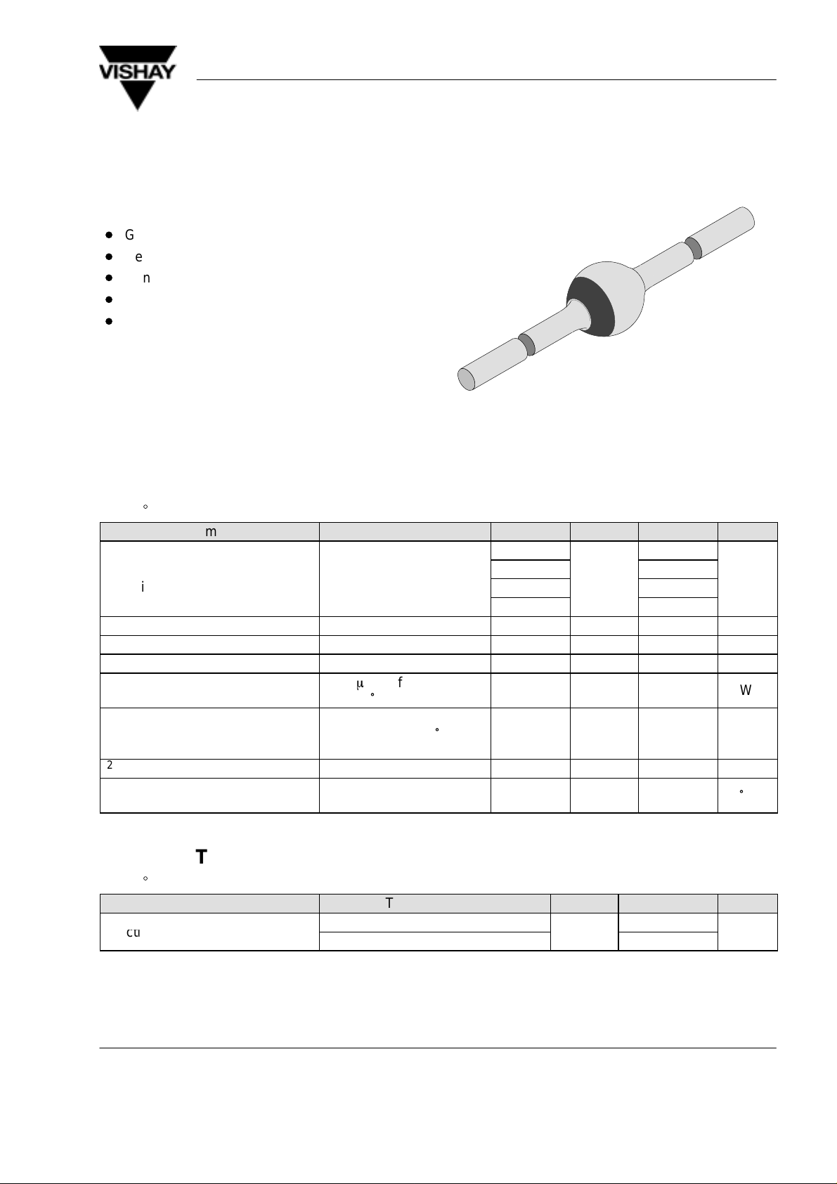
Silicon Mesa Rectifiers
g
R
V
Junction ambient
R
K/W
Features
D
Glass passivated junction
D
Hermetically sealed package
D
Controlled avalanche characteristics
D
Low reverse current
D
High surge current loading
1N5624...1N5627
Vishay Telefunken
Applications
Rectifier, general purpose
94 9588
Absolute Maximum Ratings
Tj = 25_C
Parameter Test Conditions Type Symbol Value Unit
1N5624 200
Reverse voltage=
Repetitive peak reverse voltage
Peak forward surge current tp=10ms, half sinewave I
Repetitive peak forward current I
Average forward current I
Pulse avalanche peak power
Pulse energy in avalanche mode,
non repetitive (inductive load
switch off)
i2*t–rating i2*t 40 A2*s
Junction and storage tempera-
ture range
tp=20ms, half sine wave,
T
=175 °C
j
I
=1A, Tj=175°C E
(BR)R
1N5625
1N5626
1N5627 800
VR=
V
RRM
FSM
FRM
FAV
P
Tj=T
R
R
stg
400
600
100 A
18 A
3 A
1000 W
20 mJ
–65...+175
°
C
Maximum Thermal Resistance
Tj = 25_C
Parameter Test Conditions Symbol Value Unit
l=10mm, TL=constant
on PC board with spacing 25mm
Document Number 86063
Rev. 2, 27-Sep-00
thJA
25
70
www.vishay.com
1 (4)
Page 2
1N5624...1N5627
Reverse current
I
A
Reverse recovery time
t
s
Vishay Telefunken
Electrical Characteristics
Tj = 25_C
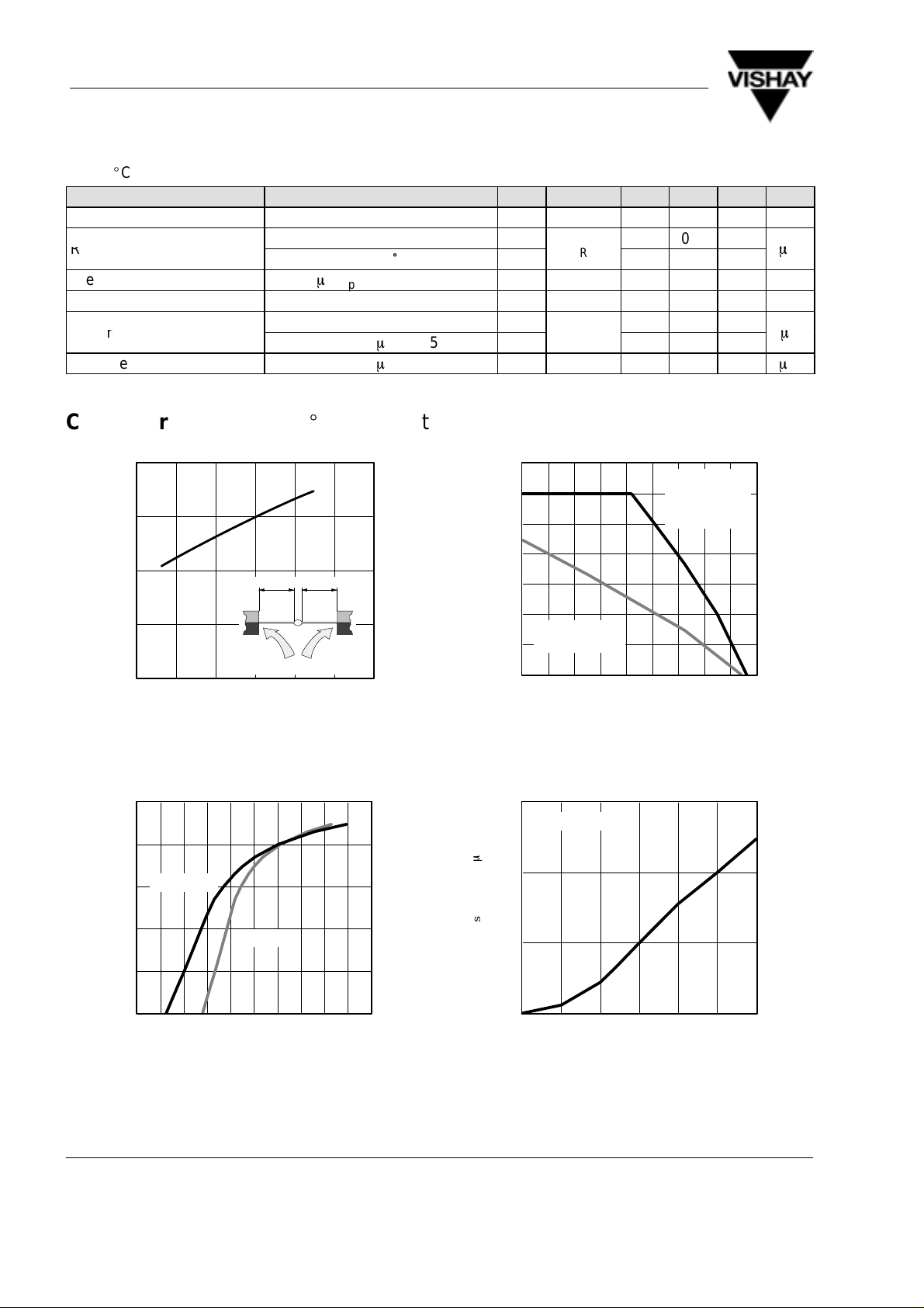
Parameter T est Conditions Type Symbol Min Typ Max Unit
Forward voltage IF=3A V
VR=V
RRM
VR=V
, Tj=100°C
RRM
Breakdown voltage IR=100mA, tp/T=0.01, tp=0.3ms V
Diode capacitance VR=4V, f=1MHz C
IF=0.5A, IR=1A, iR=0.25A
IF=1A, di/dt=5A/ms, VR=50V
Reverse recovery charge IF=1A, di/dt=5A/ms Q
Characteristics (Tj = 25_C unless otherwise specified)
F
R
(BR)
D
rr
rr
1.0 V
0.1 1
5 10
m
1600 V
40 60 pF
2 4
3 6
6 10
m
m
C
40
30
thJA
R – Therm. Resist. Junction / Ambient ( K/W )
94 9563
20
10
0
0 5 10 15 25
l – Lead Length ( mm )
ll
TL=constant
20
30
Figure 1. Max. Thermal Resistance vs. Lead Length
100.000
10.000
1.000
Tj=175°C
3.5
3.0
2.5
2.0
1.5
1.0
R
=70K/W
thJA
PCB: d=25mm
0.5
FAV
I – Average Forward Current ( A )
0
0 20 40 60 80 100 120 140 160 180
T
– Ambient Temperature ( °C )16393
amb
VR=V
RRM
half sinewave
R
=25K/W
thJA
l=10mm
Figure 3. Max. Average Forward Current vs.
Ambient Temperature
1000
VR = V
RRM
m
100
0.100
F
0.010
I – Forward Current ( A)
0.001
0 0.2 0.4 0.6 0.8 1.0 1.2 1.4 1.6 1.8 2.0
Figure 2. Forward Current vs. Forward Voltage
www.vishay.com Document Number 86063
2 (4) Rev. 2, 27-Sep-00
Tj=25°C
VF – Forward Voltage ( V )16392
10
R
I – Reverse Current ( A )
1
25 50 75 100 125 150 175
Tj – Junction Temperature ( °C )16394
Figure 4. Reverse Current vs. Junction Temperature
Page 3
1N5624...1N5627
Vishay Telefunken
300
VR = V
250
200
150
100
50
R
P – Reverse Power Dissipation ( mW )
0
25 50 75 100 125 150 175
Tj – Junction Temperature ( °C )16395
PR–Limit
@80%V
PR–Limit
@100%V
R
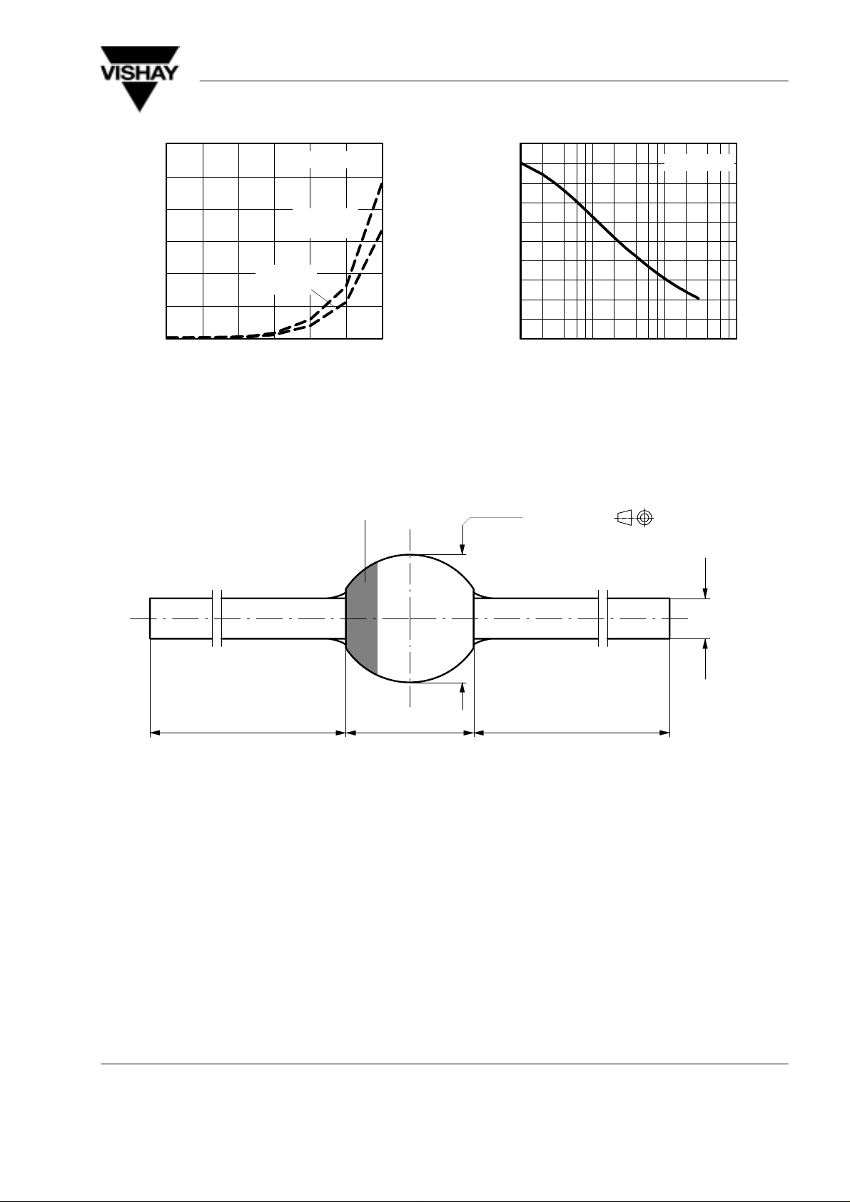
Figure 5. Max. Reverse Power Dissipation vs.
Junction Temperature
Dimensions in mm
Sintered Glass Case
SOD 64
Weight max. 1.0g
Cathode Identification
RRM
R
100
90
80
70
60
50
40
30
20
D
C – Diode Capacitance ( pF )
10
0
0.1 1.0 10.0 100.0
VR – Reverse Voltage ( V )16396
f=1MHz
Figure 6. Diode Capacitance vs. Reverse Voltage
∅ 4.3 max.
technical drawings
according to DIN
specifications
26 min. 26 min.
4.2 max.
∅ 1.35 max.
94 9587
Document Number 86063
Rev. 2, 27-Sep-00
www.vishay.com
3 (4)
Page 4

1N5624...1N5627
Vishay Telefunken
Ozone Depleting Substances Policy Statement
It is the policy of Vishay Semiconductor GmbH to
1. Meet all present and future national and international statutory requirements.
2. Regularly and continuously improve the performance of our products, processes, distribution and operating
systems with respect to their impact on the health and safety of our employees and the public, as well as their
impact on the environment.
It is particular concern to control or eliminate releases of those substances into the atmosphere which are known as
ozone depleting substances (ODSs).
The Montreal Protocol (1987) and its London Amendments (1990) intend to severely restrict the use of ODSs and
forbid their use within the next ten years. V arious national and international initiatives are pressing for an earlier ban
on these substances.
Vishay Semiconductor GmbH has been able to use its policy of continuous improvements to eliminate the use of
ODSs listed in the following documents.
1. Annex A, B and list of transitional substances of the Montreal Protocol and the London Amendments respectively
2. Class I and II ozone depleting substances in the Clean Air Act Amendments of 1990 by the Environmental
Protection Agency (EPA) in the USA
3. Council Decision 88/540/EEC and 91/690/EEC Annex A, B and C (transitional substances) respectively.
Vishay Semiconductor GmbH can certify that our semiconductors are not manufactured with ozone depleting
substances and do not contain such substances.
We reserve the right to make changes to improve technical design and may do so without further notice.
Parameters can vary in different applications. All operating parameters must be validated for each customer application
by the customer. Should the buyer use Vishay-Telefunken products for any unintended or unauthorized application, the
buyer shall indemnify Vishay-Telefunken against all claims, costs, damages, and expenses, arising out of, directly or
indirectly , any claim of personal damage, injury or death associated with such unintended or unauthorized use.
Vishay Semiconductor GmbH, P.O.B. 3535, D-74025 Heilbronn, Germany
Telephone: 49 (0)7131 67 2831, Fax number: 49 (0)7131 67 2423
www.vishay.com Document Number 86063
4 (4) Rev. 2, 27-Sep-00
 Loading...