

Page 1
DISCRETE SEMICONDUCTORS
DATA SH EET
M3D176
1N5225B to 1N5267B
Voltage regulator diodes
Product specification
Supersedes data of April 1992
1996 Apr 26
Page 2
Philips Semiconductors Product specification
Voltage regulator diodes 1N5225B to 1N5267B
FEATURES
• Total power dissipation:
max. 500 mW
• Tolerance series: ±5%
DESCRIPTION
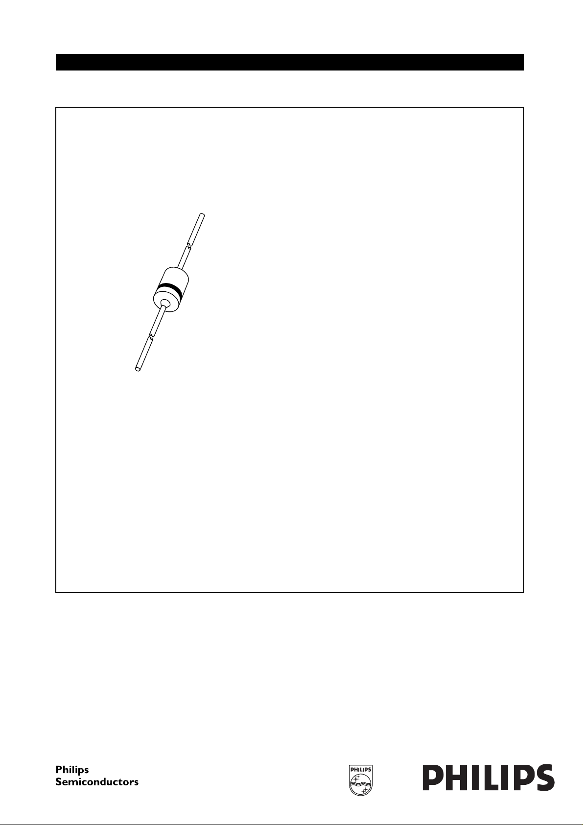
Low-power voltage regulator diodes in hermetically sealed leaded glass
SOD27 (DO-35) packages.
The series consists of 43 types with nominal working voltages from 3.0 to 75 V.
• Working voltage range:
nom. 3.0 to 75 V
• Non-repetitive peak reverse power
dissipation: max. 40 W.
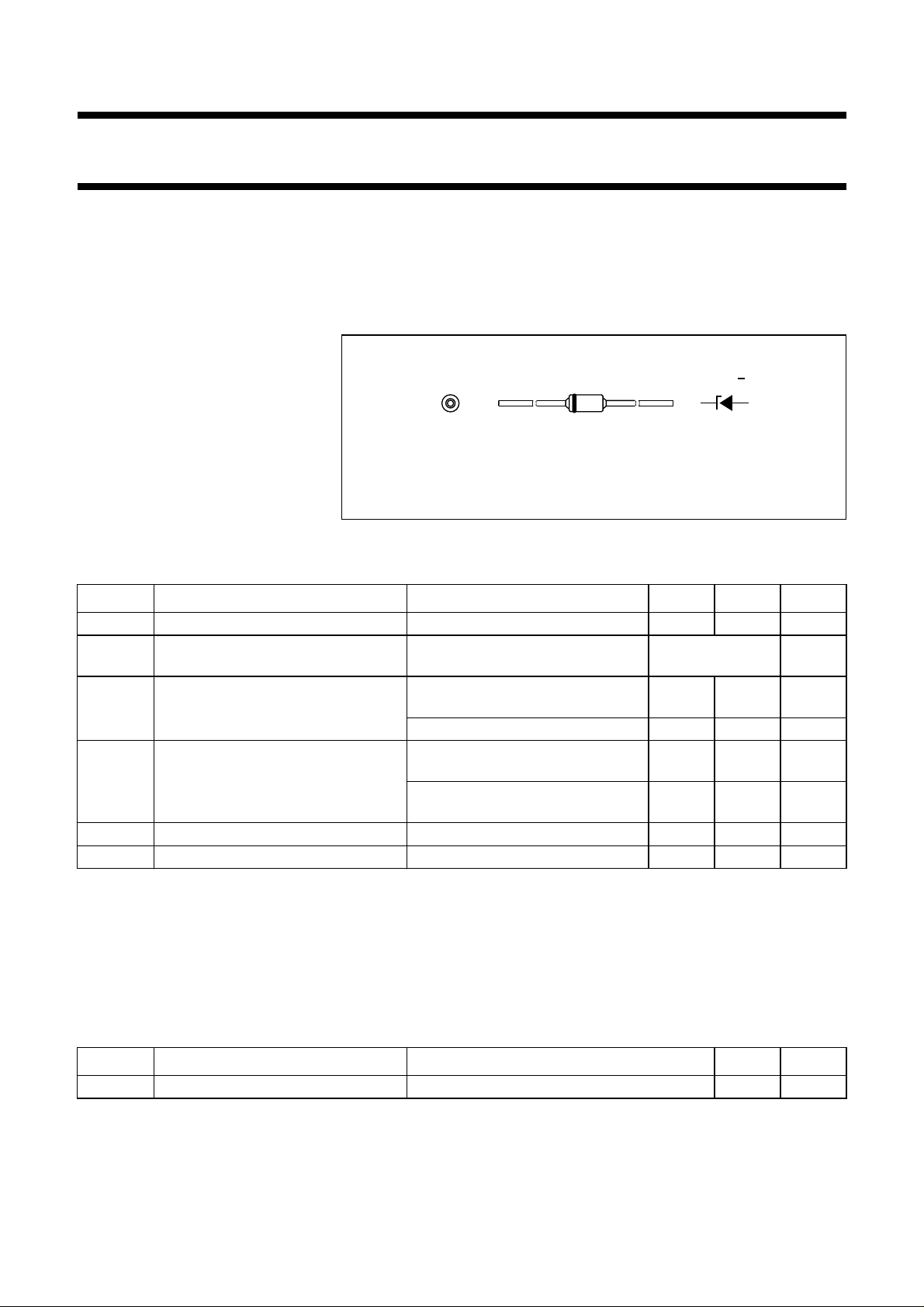
handbook, halfpage
APPLICATIONS
ka
MAM239
• Low-power voltage stabilizers or
voltage references.
The diodes are type branded.
Fig.1 Simplified outline (SOD27; DO-35) and symbol.
LIMITING VALUES
In accordance with the Absolute Maximum Rating System (IEC 134).
SYMBOL PARAMETER CONDITIONS MIN. MAX. UNIT
I
F
I
ZSM
P
tot
continuous forward current − 250 mA
non-repetitive peak reverse current tp= 100 µs; square wave;
Tj=25°C prior to surge
total power dissipation T
=50°C; lead length max.;
amb
see Table
“Per type”
− 400 mW
note 1
Lead length 8 mm; note 2 − 500 mW
P
ZSM
non-repetitive peak reverse power
dissipation
tp= 100 µs; square wave;
Tj=25°C prior to surge; see Fig.3
t
= 8.3 ms; square wave;
p
− 40 W
− 10 W
Tj≤ 55 °C prior to surge
T
stg
T
j
storage temperature −65 +200 °C
junction temperature −65 +200 °C
Notes
1. Device mounted on a printed circuit-board without metallization pad.
2. Tie-point temperature ≤ 75 °C.
ELECTRICAL CHARACTERISTICS
Table 1
=25°C; unless otherwise specified.
T
j
SYMBOL PARAMETER CONDITIONS MAX. UNIT
V
F
forward voltage IF= 200 mA; see Fig.4 1.1 V
1996 Apr 26 2
Page 3
1996 Apr 26 3
Per type
=25°C; unless otherwise specified.
T
j
Philips Semiconductors Product specification
Voltage regulator diodes 1N5225B to 1N5267B
TYPE No.
WORKING
VOLTAGE
(1)
(V)
V
Z
at I
Ztest
DIFFERENTIAL
RESISTANCE
(Ω)
r
dif
at I
Ztest
TEMP. COEFF.
(%/K)
S
Z
(2)
at I
Z
TEST
CURRENT
(mA)
I
Ztest
DIODE CAP.
Cd(pF)
at f = 1 MHz;
at VR=0V
NOM. MAX. MAX. MAX. MAX. MAX.
REVERSE CURRENT
at REVERSE
VOLTAGE
IR (µA)
V
R
(V)
NON-REPETITIVE PEAK
REVERSE CURRENT
tp= 100 µs; T
1N5225B 3.0 1600 −0.075 20 450 50 1.0 6.0
1N5226B 3.3 1600 −0.070 20 450 25 1.0 6.0
1N5227B 3.6 1700 −0.065 20 450 15 1.0 6.0
1N5228B 3.9 1900 −0.060 20 450 10 1.0 6.0
1N5229B 4.3 2000 ±0.055 20 450 5 1.0 6.0
1N5230B 4.7 1900 ±0.030 20 450 5 1.5 6.0
1N5231B 5.1 1600 ±0.030 20 300 5 2.0 6.0
1N5232B 5.6 1600 +0.038 20 300 5 3.0 6.0
1N5233B 6.0 1600 +0.038 20 300 5 3.5 6.0
1N5234B 6.2 1000 +0.045 20 200 5 4.0 6.0
1N5235B 6.8 750 +0.050 20 200 3 5.0 6.0
1N5236B 7.5 500 +0.058 20 150 3 6.0 4.0
1N5237B 8.2 500 +0.062 20 150 3 6.5 4.0
1N5238B 8.7 600 +0.065 20 150 3 6.5 3.5
1N5239B 9.1 600 +0.068 20 150 3 7.0 3.0
1N5240B 10 600 +0.075 20 90 3 8.0 3.0
1N5241B 11 600 +0.076 20 85 2 8.4 2.5
1N5242B 12 600 +0.077 20 85 1 9.1 2.5
1N5243B 13 600 +0.079 9.5 80 0.5 9.9 2.5
1N5244B 14 600 +0.082 9.0 80 0.1 10.0 2.0
1N5245B 15 600 +0.082 8.5 75 0.1 11.0 2.0
1N5246B 16 600 +0.083 7.8 75 0.1 12.0 1.5
1N5247B 17 600 +0.084 7.4 75 0.1 13.0 1.5
1N5248B 18 600 +0.085 7.0 70 0.1 14.0 1.5
1N5249B 19 600 +0.086 6.6 70 0.1 14.0 1.5
1N5250B 20 600 +0.086 6.2 60 0.1 15.0 1.5
I
ZSM
(A)
amb
=25°C
Page 4

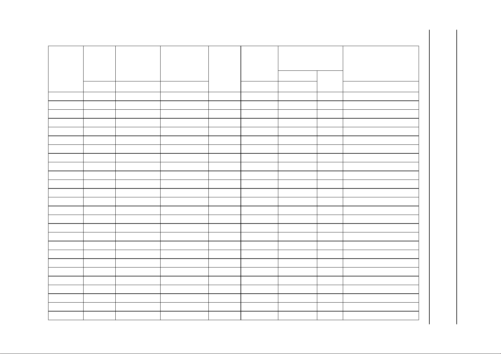
1996 Apr 26 4
TYPE No.
WORKING
VOLTAGE
V
(V)
Z
at I
Ztest
NOM. MAX. MAX. MAX. MAX. MAX.
DIFFERENTIAL
RESISTANCE
(1)
r
dif
at I
(Ω)
Ztest
TEMP. COEFF.
SZ (%/K)
(2)
at I
Z
TEST
CURRENT
I
(mA)
Ztest
DIODE CAP.
Cd(pF)
at f = 1 MHz;
at VR=0V
REVERSE CURRENT
at REVERSE
VOLTAGE
IR (µA)
V
R
(V)
1N5251B 22 600 +0.087 5.6 60 0.1 17.0 1.25
1N5252B 24 600 +0.088 5.2 55 0.1 18.0 1.25
1N5253B 25 600 +0.089 5.0 55 0.1 19.0 1.25
1N5254B 27 600 +0.090 4.6 50 0.1 21.0 1.0
1N5255B 28 600 +0.091 4.5 50 0.1 21.0 1.0
1N5256B 30 600 +0.091 4.2 50 0.1 23.0 1.0
1N5257B 33 700 +0.092 3.8 45 0.1 25.0 0.9
1N5258B 36 700 +0.093 3.4 45 0.1 27.0 0.8
1N5259B 39 800 +0.094 3.2 45 0.1 30.0 0.7
1N5260B 43 900 +0.095 3.0 40 0.1 33.0 0.6
1N5261B 47 1000 +0.095 2.7 40 0.1 36.0 0.5
1N5262B 51 1100 +0.096 2.5 40 0.1 39.0 0.4
1N5263B 56 1300 +0.096 2.2 40 0.1 43.0 0.3
1N5264B 60 1400 +0.097 2.1 40 0.1 46.0 0.3
1N5265B 62 1400 +0.097 2.0 35 0.1 47.0 0.3
1N5266B 68 1600 +0.097 1.8 35 0.1 52.0 0.25
1N5267B 75 1700 +0.098 1.7 35 0.1 56.0 0.2
NON-REPETITIVE PEAK
REVERSE CURRENT
I
(A)
ZSM
tp= 100 µs; T
amb
=25°C
Philips Semiconductors Product specification
Voltage regulator diodes 1N5225B to 1N5267B
Notes
1. VZ is measured with device at thermal equilibrium while held in clips at 10 mm from body in still air at 25 °C.
2. For types 1N5225B to 1N5242B the IZcurrent is 7.5 mA; for 1N5243B and higher IZ=I
. SZ values valid between 25 °C and 125 °C.
Ztest
Page 5

Philips Semiconductors Product specification
Voltage regulator diodes 1N5225B to 1N5267B
THERMAL CHARACTERISTICS
SYMBOL PARAMETER CONDITIONS VALUE UNIT
R
th j-tp
R
th j-a
Note
1. Device mounted on a printed circuit-board without metallization pad.
thermal resistance from junction to tie-point lead length 10 mm 300 K/W
thermal resistance from junction to ambient lead length max.; see Fig.2 and note 1 380 K/W
1996 Apr 26 5
Page 6

Philips Semiconductors Product specification
Voltage regulator diodes 1N5225B to 1N5267B
GRAPHICAL DATA
3
10
handbook, full pagewidth
R
th j-a
(K/W)
2
10
10
1
−1
10
δ = 1
0.75
0.50
0.33
0.20
0.10
0.05
0.02
0.01
≤0.001
t
p
T
11010
2103
4
10
Fig.2 Thermal resistance from junction to ambient as a function of pulse duration.
δ =
tp (ms)
MBG930
t
p
T
5
10
3
10
handbook, halfpage
P
ZSM
(W)
2
10
10
1
−1
10
(1) Tj=25°C (prior to surge).
(2) Tj= 150°C (prior to surge).
(1)
(2)
1 duration (ms)
Fig.3 Maximum permissible non-repetitive
peak reverse power dissipation
versus duration.
MBG801
250
handbook, halfpage
I
F
(mA)
125
0
10
0.5 1.0
Tj=25°C.
0.75 VF (V)
MBG803
Fig.4 Forward current as a function of forward
voltage; typical values.
1996 Apr 26 6
Page 7

Philips Semiconductors Product specification
Voltage regulator diodes 1N5225B to 1N5267B
PACKAGE OUTLINE
dbook, full pagewidth
Dimensions in mm.
1.85
max
25.4 min
4.25
max
25.4 min
0.56
max
MLA428 - 1
Fig.5 SOD27 (DO-35).
DEFINITIONS
Data sheet status
Objective specification This data sheet contains target or goal specifications for product development.
Preliminary specification This data sheet contains preliminary data; supplementary data may be published later.
Product specification This data sheet contains final product specifications.
Limiting values
Limiting values given are in accordance with the Absolute Maximum Rating System (IEC 134). Stress above one or
more of the limiting values may cause permanent damage to the device. These are stress ratings only and operation
of the device at these or at any other conditions above those given in the Characteristics sections of the specification
is not implied. Exposure to limiting values for extended periods may affect device reliability.
Application information
Where application information is given, it is advisory and does not form part of the specification.
LIFE SUPPORT APPLICATIONS
These products are not designed for use in life support appliances, devices, or systems where malfunction of these
products can reasonably be expected to result in personal injury. Philips customers using or selling these products for
use in such applications do so at their own risk and agree to fully indemnify Philips for any damages resulting from such
improper use or sale.
1996 Apr 26 7
 Loading...