

Page 1
1N4728A - 1N4758A
Zener Diodes
Tolerance = 5%
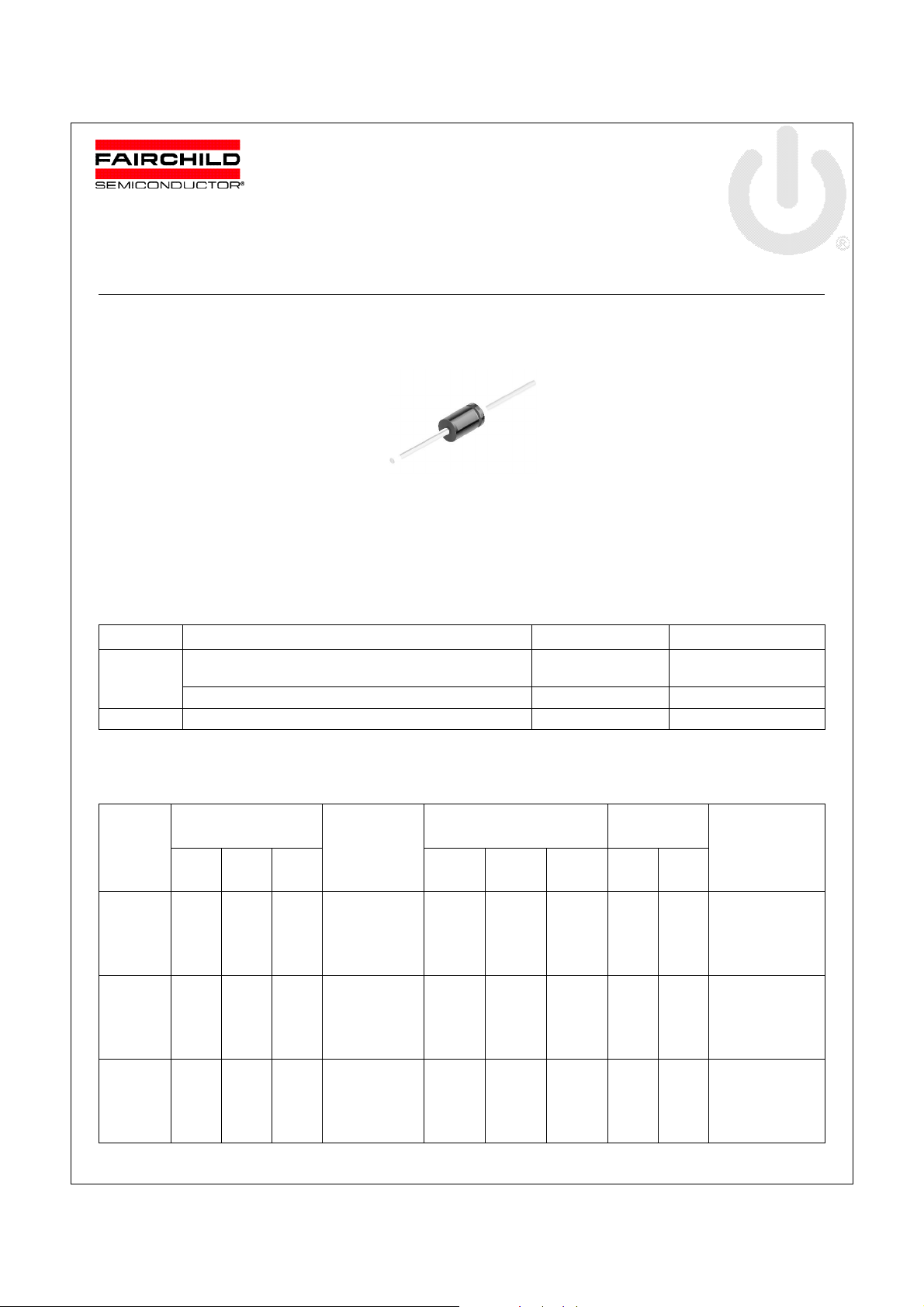
DO-41 Glass case
COLOR BAND DENOTE S CATHODE
1N4728A - 1N4758A — Zener Diodes
April 2009
Absolute Maximum Ratings * T
= 25°C unless otherwise noted
a
Symbol Parameter Value Units
P
TJ, T
* These ratings are limiting values above which the serviceability of the diode may be impaired.
Electrical Characteristics T
Device
1N4728A
1N4729A
1N4730A
1N4731A
1N4732A
1N4733A
1N4734A
1N4735A
1N4736A
1N4737A
1N4738A
1N4739A
1N4740A
1N4741A
1N4742A
Power Dissipation
D
@ TL 50C, Lead Length = 3/8”
Derate above 50C 6.67 mW/C
Operating and Storage Temperature Range -65 to +200 C
STG
= 25°C unless otherwise noted
a
VZ (V) @ IZ (Note 1)
Min. Typ. Max.
3.135
3.42
3.705
4.085
4.465
4.845
5.32
5.89
6.46
7.125
7.79
8.645
9.5
10.45
11.4
3.3
3.6
3.9
4.3
4.7
5.1
5.6
6.2
6.8
7.5
8.2
9.1
10
11
12
3.465
3.78
4.095
4.515
4.935
5.355
5.88
6.51
7.14
7.875
8.61
9.555
10.5
11.55
12.6
Test Current
IZ (mA)
76
69
64
58
53
49
45
41
37
34
31
28
25
23
21
Max. Zener Impedance
ZZ @ IZ
()
3.5
4.5
10
10
ZZK @
I
()
ZK
400
400
9
9
8
7
5
2
4
5
7
8
9
400
400
500
550
600
700
700
700
700
700
700
700
700
1.0 W
Leakage
Current
I
ZK
(mA)
1
1
1
1
1
1
1
1
1
0.5
0.5
0.5
0.25
0.25
0.25
IR
(A)
100
100
50
10
10
10
10
10
10
10
10
10
10
5
5
Non-Repetitive
V
R
(V)
I
1
1
1
1
1
1
2
3
4
5
6
7
7.6
8.4
9.1
Peak Reverse
ZSM
Current
(mA)
(Note 2)
1380
1260
1190
1070
970
890
810
730
660
605
550
500
454
414
380
© 2009 Fairchild Semiconductor Corporation www.fairchildsemi.com
1N4728A - 1N4758A Rev. H3 1
Page 2
1N4728A - 1N4758A — Zener Diodes
VZ (V) @ IZ (Note 1)
13.65
15.75
16.8
18.9
21
23.1
25.2
28.35
31.5
34.65
37.8
40.95
45.15
49.35
53.55
Test Current
IZ (mA)
19
17
15.5
14
12.5
11.5
10.5
9.5
8.5
7.5
7
6.5
6
5.5
5
Device
Min. Typ. Max.
1N4743A
1N4744A
1N4745A
1N4746A
1N4747A
1N4748A
1N4749A
1N4750A
1N4751A
1N4752A
1N4753A
1N4754A
1N4755A
1N4756A
1N4757A
1N4758A 53.2 56 58.8 4.5 110 2000 0.25 5 42.6 80
Notes:
1. Zener Voltage (VZ)
The zener voltage is measured with the device junction in the thermal equilibrium at the lead temperature (TL) at 30C ± 1C and 3/8” lead length.
2. 2 Square wave Reverse Surge at 8.3 msec soak time.
12.35
14.25
15.2
17.1
19
20.9
22.8
25.65
28.5
31.35
34.2
37.05
40.85
44.65
48.45
13
15
16
18
20
22
24
27
30
33
36
39
43
47
51
Max. Zener Impedance
ZZ @ IZ
()
10
14
16
20
22
23
25
35
40
45
50
60
70
80
95
ZZK @
IZK ()
700
700
700
750
750
750
750
750
1000
1000
1000
1000
1500
1500
1500
I
ZK
(mA)
0.25
0.25
0.25
0.25
0.25
0.25
0.25
0.25
0.25
0.25
0.25
0.25
0.25
0.25
0.25
Leakage
Current
IR
(A)
5
5
5
5
5
5
5
5
5
5
5
5
5
5
5
V
(V)
9.9
11.4
12.2
13.7
15.2
16.7
18.2
20.6
22.8
25.1
27.4
29.7
32.7
35.8
38.8
R
Non-Repetitive
Peak Reverse
Current
I
(mA)
ZSM
Top Mark Information
344
304
285
250
225
205
190
170
150
135
125
115
110
95
90
(Note 2)
Device Line 1 Line 2 Line 3 Line 4 Line 5
1N4728A
1N4729A
1N4730A
1N4731A
1N4732A
1N4733A
1N4734A
1N4735A
1N4736A
1N4737A
1N4738A
1N4739A
1N4740A
1N4741A
1N4742A
1N4743A
1N4744A
1N4745A
1N4746A
1N4747A
1N4748A
1N4749A
1N4750A
1N4751A
1N4752A
1N4753A
1N4754A
1N4755A
1N4756A
1N4757A
1N4758A LOGO 47 58 A XY
LOGO
LOGO
LOGO
LOGO
LOGO
LOGO
LOGO
LOGO
LOGO
LOGO
LOGO
LOGO
LOGO
LOGO
LOGO
LOGO
LOGO
LOGO
LOGO
LOGO
LOGO
LOGO
LOGO
LOGO
LOGO
LOGO
LOGO
LOGO
LOGO
LOGO
47
47
47
47
47
47
47
47
47
47
47
47
47
47
47
47
47
47
47
47
47
47
47
47
47
47
47
47
47
47
28
29
30
31
32
33
34
35
36
37
38
39
40
41
42
43
44
45
46
47
48
49
50
51
52
53
54
55
56
57
A
A
A
A
A
A
A
A
A
A
A
A
A
A
A
A
A
A
A
A
A
A
A
A
A
A
A
A
A
A
XY
XY
XY
XY
XY
XY
XY
XY
XY
XY
XY
XY
XY
XY
XY
XY
XY
XY
XY
XY
XY
XY
XY
XY
XY
XY
XY
XY
XY
XY
© 2009 Fairchild Semiconductor Corporation www.fairchildsemi.com
1N4728A - 1N4758A Rev. H3 2
Page 3
Top Mark Information (Continued)
1N4728A - 1N4758A — Zener Diodes
F
47
36
A
XY
F
1st line: F - Fairchild Logo
2nd line: Device Name - 3rd to 4th characters of device name for 1Nxx series
or 4th to 6th characters for BZXyy series
3rd line: Device Name - 5th to 6th characters of device name for 1Nxx series
or Voltage rating for BZXyy series
4th line: Device Name - 7th to 8th characters of device name for 1Nxx series
or Large Die identification only for BZXyy series
5th line: Date Code - Two Digit - Six Weeks Date Code
General Requirements:
1.0 Cathode Band
2.0 First Line: F - Fairchild Logo
3.0 Second Line: Device name - For 1Nxx series: 3rd to 4th characters of the device name.
4.0 Third Line: Device name - For 1Nxx series: 5th to 6th characters of the device name.
5.0 Third Line: Device name - For 1Nxx series: 7th to 8th characters of the device name.
6.0 Fourth Line: Date Code - Two Digit - Six Weeks Date Code
7.0 Devices shall be marked as required in the device specification (PID or FSC Test Spec).
8.0 Maximum no. of marking lines: 5
9.0 Maximum no. of digits per line: 3
10.0 FSC logo must be 20 % taller than the alphanumeric marking and should occupy the 2 characters of the specified line.
11.0 Marking Font: Arial (Except FSC Logo)
12.0 First character of each marking line must be aligned vertically.
13.0 All device markings must be based on Fairchild device specification.
For BZxx series: 4th to 6th characters of the device name.
For BZXyy series: Voltage rating
(the 8th character is the large die identification)
For BZXyy series: Large Die Identification character
Where: X represents the last digit of the calendar year
Y represents the Six weeks numeric code
© 2009 Fairchild Semiconductor Corporation www.fairchildsemi.com
1N4728A - 1N4758A Rev. H3 3
Page 4
 Loading...