

Page 1
MOTOROLA
SEMICONDUCTOR
TECHNICAL DATA
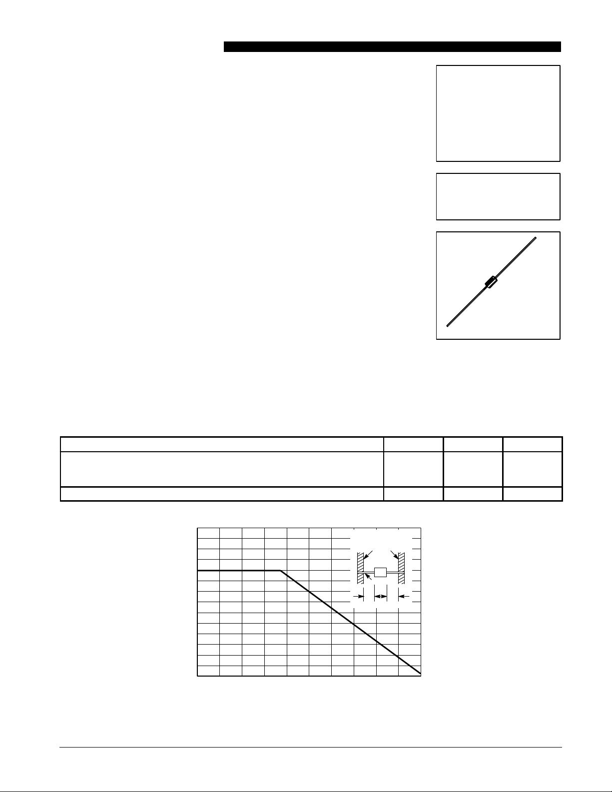
500 mW DO-35 Glass
Zener Voltage Regulator Diodes
GENERAL DATA APPLICABLE TO ALL SERIES IN
THIS GROUP
500 Milliwatt
Hermetically Sealed
Glass Silicon Zener Diodes
Specification Features:
• Complete Voltage Range — 1.8 to 200 Volts
• DO-204AH Package — Smaller than Conventional DO-204AA Package
• Double Slug Type Construction
• Metallurgically Bonded Construction
Mechanical Characteristics:
CASE: Double slug type, hermetically sealed glass
MAXIMUM LEAD TEMPERATURE FOR SOLDERING PURPOSES: 230°C, 1/16″ from
case for 10 seconds
FINISH: All external surfaces are corrosion resistant with readily solderable leads
POLARITY: Cathode indicated by color band. When operated in zener mode, cathode
will be positive with respect to anode
MOUNTING POSITION: Any
WAFER FAB LOCATION: Phoenix, Arizona
ASSEMBLY/TEST LOCATION: Seoul, Korea
GENERAL
DATA
500 mW
DO-35 GLASS
GLASS ZENER DIODES
500 MILLIWATTS
1.8–200 VOL TS
CASE 299
DO-204AH
GLASS
MAXIMUM RATINGS
DC Power Dissipation and TL ≤ 75°C
Lead Length = 3/8″
Derate above TL = 75°C
Operating and Storage Temperature Range TJ, T
* Some part number series have lower JEDEC registered ratings.
(Motorola Devices)*
Rating
0.7
0.6
0.5
0.4
0.3
0.2
0.1
, MAXIMUM POWER DISSIPATION (WA TTS)
D
P
0
0 20 40 60 80 100 120 140 160 180 200
HEAT
SINKS
3/8” 3/8”
TL, LEAD TEMPERATURE (
Figure 1. Steady State Power Derating
°
C)
Symbol Value Unit
P
D
stg
500
4
– 65 to +200 °C
mW
mW/°C
Motorola TVS/Zener Device Data
500 mW DO-35 Glass Data Sheet
6-97
Page 2
GENERAL DATA — 500 mW DO-35 GLASS
APPLICATION NOTE — ZENER VOLTAGE
Since the actual voltage available from a given zener diode
is temperature dependent, it is necessary to determine junction temperature under any set of operating conditions in order
to calculate its value. The following procedure is recommended:
Lead Temperature, TL, should be determined from:
TL = θLAPD + TA.
θLA is the lead-to-ambient thermal resistance (°C/W) and PD is
the power dissipation. The value for θLA will vary and depends
on the device mounting method. θLA is generally 30 to 40°C/W
for the various clips and tie points in common use and for
printed circuit board wiring.
The temperature of the lead can also be measured using a
thermocouple placed on the lead as close as possible to the tie
point. The thermal mass connected to the tie point is normally
large enough so that it will not significantly respond to heat
surges generated in the diode as a result of pulsed operation
once steady-state conditions are achieved. Using the measured value of TL, the junction temperature may be determined by:
TJ = TL + ∆TJL.
∆TJL is the increase in junction temperature above the lead
temperature and may be found from Figure 2 for dc power:
∆TJL = θJLPD.
For worst-case design, using expected limits of IZ, limits of
PD and the extremes of TJ(∆TJ) may be estimated. Changes in
voltage, VZ, can then be found from:
∆V = θVZTJ.
θVZ, the zener voltage temperature coefficient, is found from
Figures 4 and 5.
Under high power-pulse operation, the zener voltage will
vary with time and may also be affected significantly by the
zener resistance. For best regulation, keep current excursions
as low as possible.
Surge limitations are given in Figure 7. They are lower than
would be expected by considering only junction temperature,
as current crowding effects cause temperatures to be extremely high in small spots, resulting in device degradation
should the limits of Figure 7 be exceeded.
500
400
LL
300
200
100
0
0 0.2 0.4 0.6 0.8 1
, JUNCTION-TO-LEAD THERMAL RESISTANCE ( C/W)
JL
θ °
2.4–60 V
62–200 V
L, LEAD LENGTH TO HEA T SINK (INCH)
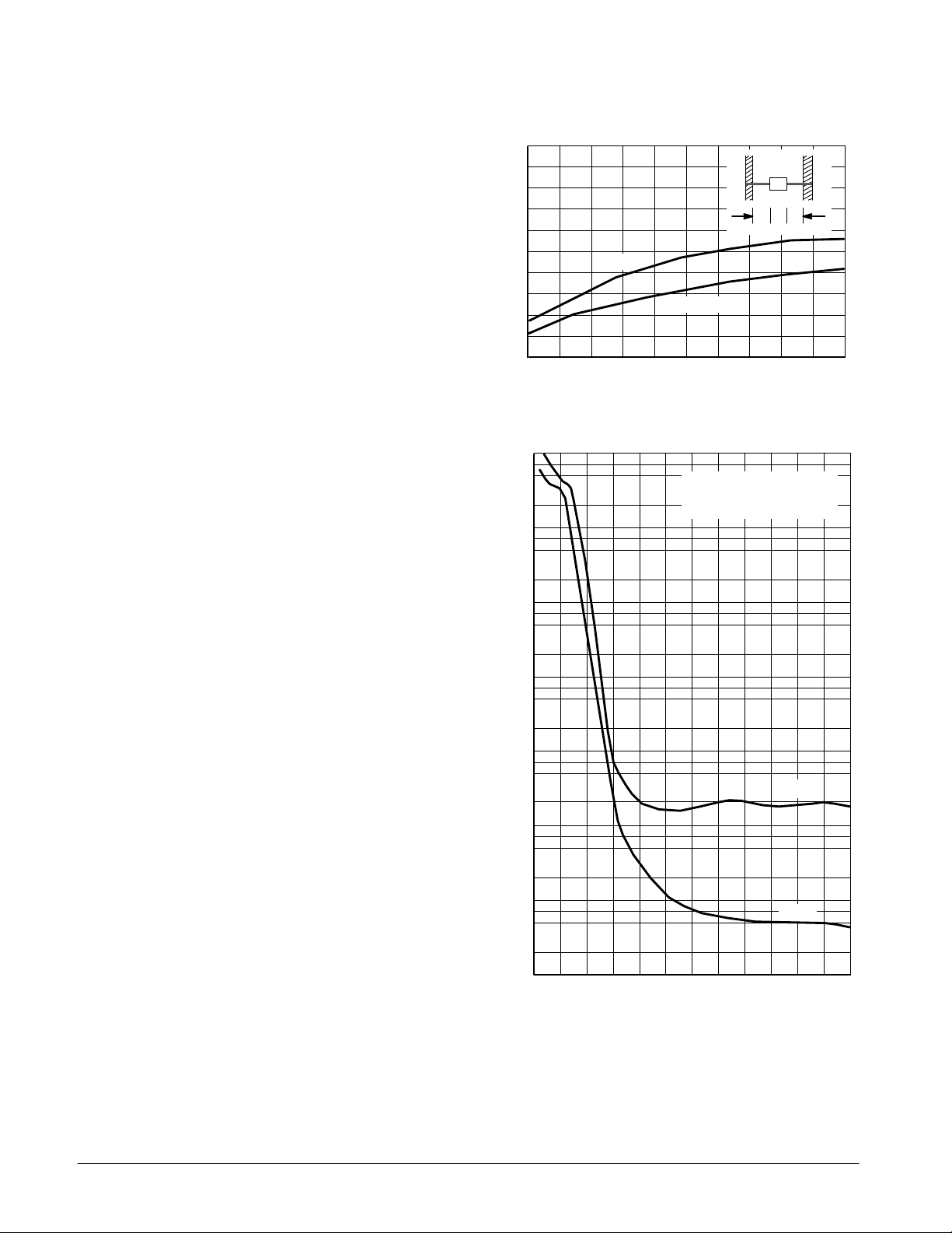
Figure 2. T ypical Thermal Resistance
1000
7000
5000
2000
1000
µ
R
I , LEAKAGE CURRENT ( A)
700
500
200
100
70
50
20
10
0.7
0.5
0.2
0.1
0.07
0.05
7
5
2
1
TYPICAL LEAKAGE CURRENT
AT 80% OF NOMINAL
BREAKDOWN VOLTAGE
+125°C
500 mW DO-35 Glass Data Sheet
6-98
0.02
0.01
0.007
0.005
0.002
0.001
34 5 678 9101112131415
VZ, NOMINAL ZENER VOLTAGE (VOLTS)
+25°C
Figure 3. T ypical Leakage Current
Motorola TVS/Zener Device Data
Page 3
GENERAL DATA — 500 mW DO-35 GLASS
TEMPERATURE COEFFICIENTS
(–55°C to +150°C temperature range; 90% of the units are in the ranges indicated.)
+12
C)
°
+10
+8
+6
+4
+2
0
, TEMPERATURE COEFFICIENT (mV/
–2
Z
V
θ
–4
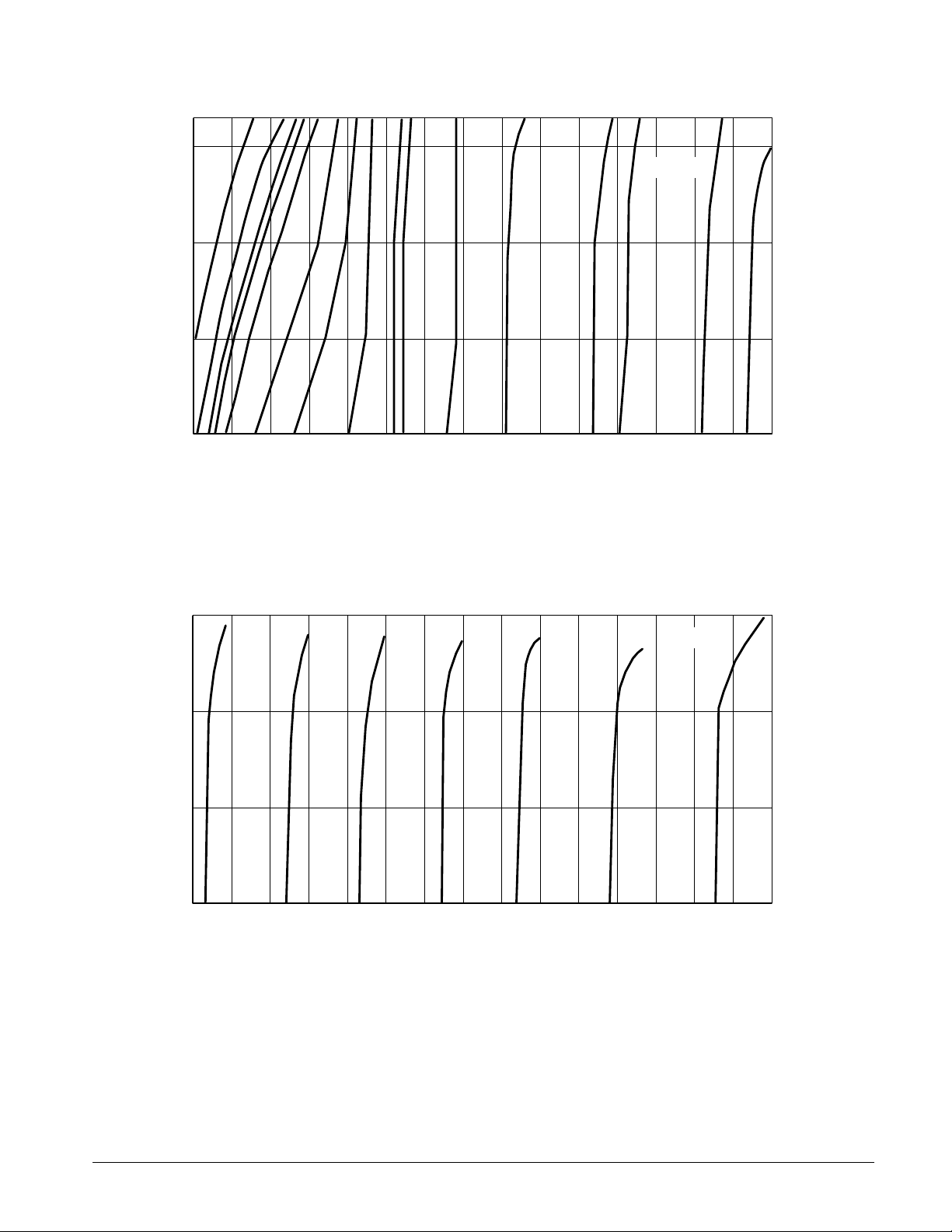
2 3 4 5 6 7 8 9 10 11 12 10 20 30 50 70 100
2345 6789101112
V
, ZENER VOLTAGE (VOLTS)
Z
RANGE
VZ@I
ZT
(NOTE 2)
Figure 4a. Range for Units to 12 Volts
200
C)
°
180
160
100
C)
°
70
50
30
20
10
, TEMPERATURE COEFFICIENT (mV/
Z
V
θ
+6
C)
°
+4
+2
RANGE
7
5
3
2
1
VZ, ZENER VOLTAGE (VOLTS)
Figure 4b. Range for Units 12 to 100 V olts
VZ@I
Z
TA=25
°
C
20 mA
VZ@IZ(NOTE 2)
140
VZ@I
120
, TEMPERATURE COEFFICIENT (mV/
Z
V
θ
100
120 130 140 150 160 170 180 190 200
VZ, ZENER VOLTAGE (VOLTS)
ZT
(NOTE 2)
Figure 4c. Range for Units 120 to 200 V olts
1000
500
200
100
50
20
10
C, CAPACITANCE (pF)
5
2
1
1 2 5 10 20 50 100
0 V BIAS
50% OF
VZBIAS
VZ, ZENER VOLTAGE (VOLTS)
TA=25°C
1 V BIAS
Figure 6a. Typical Capacitance 2.4–100 Volts
0
–2
, TEMPERATURE COEFFICIENT (mV/
Z
V
θ
–4
34 56 78
NOTE: BELOW 3 VOLTS AND ABOVE 8 VOLTS
NOTE: CHANGES IN ZENER CURRENT DO NOT
NOTE: AFFECT TEMPERATURE COEFFICIENTS
V
, ZENER VOLTAGE (VOLTS)
Z
0.01 mA
1mA
Figure 5. Effect of Zener Current
100
70
50
30
20
10
7
5
C, CAPACITANCE (pF)
3
2
1
120 140 160 180 190 200 220
0 BIAS
1 VOLTBIAS
50% OF VZBIAS
VZ, ZENER VOLTAGE (VOLTS)
TA=25°C
Figure 6b. Typical Capacitance 120–200 Volts
Motorola TVS/Zener Device Data
500 mW DO-35 Glass Data Sheet
6-99
Page 4
GENERAL DATA — 500 mW DO-35 GLASS
100
70
50
30
20
10
7
5
3
, PEAK SURGE POWER (WATTS)
2
pk
P
1
0.01 0.02 0.05 0.1 0.2 0.5 1 2 5 10 20 50 100 200 500 1000
5% DUTY CYCLE
10% DUTY CYCLE
20% DUTY CYCLE
11V–91 V NONREPETITIVE
1.8 V–10 V NONREPETITIVE
PW, PULSE WIDTH (ms)
RECTANGULAR
WAVEFORM
°
C PRIOR TO
TJ=25
INITIAL PULSE
Figure 7a. Maximum Surge Power 1.8–91 V olts
1000
700
500
300
200
100
70
50
30
20
10
7
, PEAK SURGE POWER (WATTS)
5
pk
3
P
2
1
0.01 0.1 1 10 100 1000
100–200 VOL TS NONREPETITIVE
PW, PULSE WIDTH (ms)
RECTANGULAR
WAVEFORM, TJ=25
Figure 7b. Maximum Surge Power DO-204AH
100–200 V olts
°
C
1000
500
200
100
50
20
10
5
, DYNAMIC IMPEDANCE (OHMS)
Z
Z
2
1
0.1 0.2 0.5 1 2 5 10 20 50 100
VZ= 2.7 V
47 V
27 V
6.2 V
IZ, ZENER CURRENT (mA)
TJ=25°C
iZ(rms) = 0.1 IZ(dc)
f = 60 Hz
Figure 8. Effect of Zener Current on
Zener Impedance
1000
700
500
200
100
, DYNAMIC IMPEDANCE (OHMS)
Z
Z
IZ=1mA
70
50
20
10
7
5
2
1
1 2 3 5 7 10 20 30 50 70 100
5mA
20 mA
VZ, ZENER VOLTAGE (VOLTS)
TJ=25°C
iZ(rms) = 0.1 IZ(dc)
f = 60 Hz
1000
500
200
100
50
20
10
, FORWARD CURRENT (mA)
5
150°C
F
I
2
1
0.4 0.5 0.6 0.7 0.8 0.9 1 1.1
MAXIMUM
MINIMUM
75°C
25°C
VF, FORWARD VOLTAGE (VOLTS)
Figure 9. Effect of Zener V oltage on Zener Impedance Figure 10. Typical Forward Characteristics
500 mW DO-35 Glass Data Sheet
Motorola TVS/Zener Device Data
6-100
0°C
Page 5
GENERAL DATA — 500 mW DO-35 GLASS
20
10
T
=25
°
A
1
, ZENER CURRENT (mA)
Z
I
0.1
0.01
1 23456 78910111213141516
VZ, ZENER VOLTAGE (VOLTS)
Figure 11. Zener Voltage versus Zener Current — VZ = 1 thru 16 Volts
10
TA=25
1
, ZENER CURRENT (mA)
0.1
Z
I
0.01
15 16 17 18 19 20 21 22 23 24 25 26 27 28 29 30
VZ, ZENER VOLTAGE (VOLTS)
Figure 12. Zener V oltage versus Zener Current — VZ = 15 thru 30 Volts
°
Motorola TVS/Zener Device Data
500 mW DO-35 Glass Data Sheet
6-101
Page 6
GENERAL DATA — 500 mW DO-35 GLASS
10
1
0.1
, ZENER CURRENT (mA)I
Z
I
0.01
30 35 40 45 50 55 60 70 75 80 85 90 95 100
65 105
VZ, ZENER VOLTAGE (VOLTS)
TA=25
Figure 13. Zener V oltage versus Zener Current — VZ = 30 thru 105 V olts
°
10
1
0.1
, ZENER CURRENT (mA)
Z
0.01
110 120 130 140 150 160 170 180 190 200 210 220 230 240 250 260
VZ, ZENER VOLTAGE (VOLTS)
Figure 14. Zener V oltage versus Zener Current — VZ = 110 thru 220 Volts
500 mW DO-35 Glass Data Sheet
6-102
Motorola TVS/Zener Device Data
Page 7
GENERAL DATA — 500 mW DO-35 GLASS
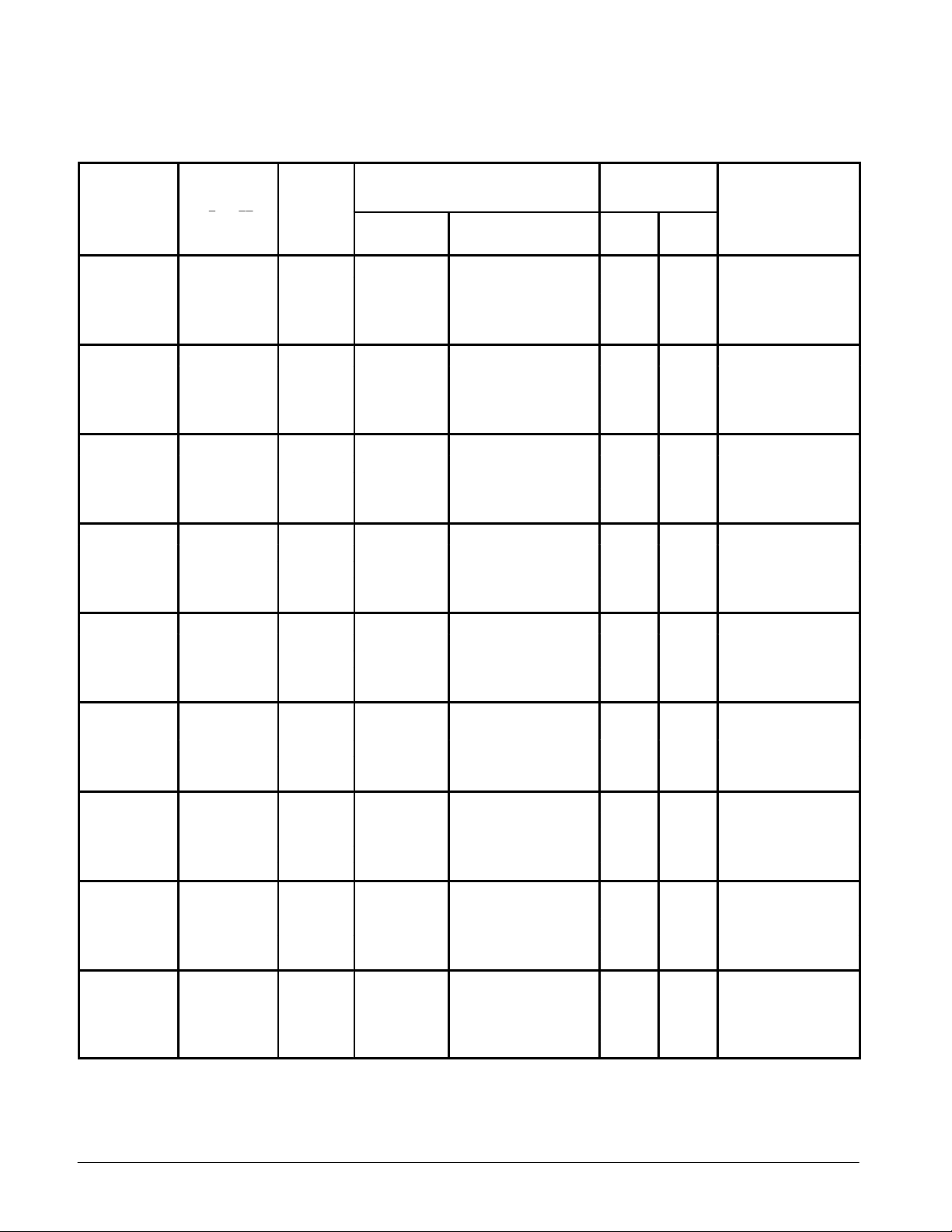
Z
Test
Maxi
DC Z
t
T
V
C
t
I
ELECTRICAL CHARACTERISTICS
Nominal
Type
Number
(Note 1)
1N4370A 2.4 20 30 150 100 200
1N4371A 2.7 20 30 135 75 150
1N4372A 3 20 29 120 50 100
ener Voltage
VZ @ I
ZT
(Note 2)
Volts
Current
(TA = 25°C, VF = 1.5 V Max at 200 mA for all types)
mum Zener Impedance
ZZT @ I
ZT
I
ZT
mA
(Note 3)
Ohms
Maximum
ener Curren
I
ZM
(Note 4)
mA
Maximum Reverse Leakage Current
TA = 25°C
IR @ VR = 1 V
µA
TA = 150°C
IR @ VR = 1 V
1N746A 3.3 20 28 110 10 30
1N747A 3.6 20 24 100 10 30
1N748A 3.9 20 23 95 10 30
1N749A 4.3 20 22 85 2 30
1N750A 4.7 20 19 75 2 30
1N751A 5.1 20 17 70 1 20
1N752A 5.6 20 11 65 1 20
1N753A 6.2 20 7 60 0.1 20
1N754A 6.8 20 5 55 0.1 20
1N755A 7.5 20 6 50 0.1 20
1N756A 8.2 20 8 45 0.1 20
1N757A 9.1 20 10 40 0.1 20
1N758A 10 20 17 35 0.1 20
1N759A 12 20 30 30 0.1 20
Nominal
ype
Number
(Note 1)
1N957B 6.8 18.5 4.5 700 1 47 150 5.2
1N958B 7.5 16.5 5.5 700 0.5 42 75 5.7
1N959B 8.2 15 6.5 700 0.5 38 50 6.2
1N960B 9.1 14 7.5 700 0.5 35 25 6.9
1N961B 10 12.5 8.5 700 0.25 32 10 7.6
1N962B 11 11.5 9.5 700 0.25 28 5 8.4
1N963B 12 10.5 11.5 700 0.25 26 5 9.1
1N964B 13 9.5 13 700 0.25 24 5 9.9
1N965B 15 8.5 16 700 0.25 21 5 11.4
1N966B 16 7.8 17 700 0.25 19 5 12.2
1N967B 18 7 21 750 0.25 17 5 13.7
1N968B 20 6.2 25 750 0.25 15 5 15.2
1N969B 22 5.6 29 750 0.25 14 5 16.7
1N970B 24 5.2 33 750 0.25 13 5 18.2
1N971B 27 4.6 41 750 0.25 11 5 20.6
1N972B 30 4.2 49 1000 0.25 10 5 22.8
1N973B 33 3.8 58 1000 0.25 9.2 5 25.1
1N974B 36 3.4 70 1000 0.25 8.5 5 27.4
1N975B 39 3.2 80 1000 0.25 7.8 5 29.7
1N976B 43 3 93 1500 0.25 7 5 32.7
1N977B 47 2.7 105 1500 0.25 6.4 5 35.8
1N978B 51 2.5 125 1500 0.25 5.9 5 38.8
1N979B 56 2.2 150 2000 0.25 5.4 5 42.6
1N980B 62 2 185 2000 0.25 4.9 5 47.1
Zener Voltage
Z
(Note 2)
Volts
Test
urren
I
ZT
mA
Maximum Zener Impedance
ZZT @ I
Ohms
ZT
(Note 3)
ZZK @ I
Ohms
ZK
I
ZK
mA
Maximum
DC Zener Current
ZM
(Note 4)
mA
Maximum Reverse Current
IR MaximumµATest Voltage Vdc
µA
V
R
Motorola TVS/Zener Device Data
500 mW DO-35 Glass Data Sheet
6-103
Page 8
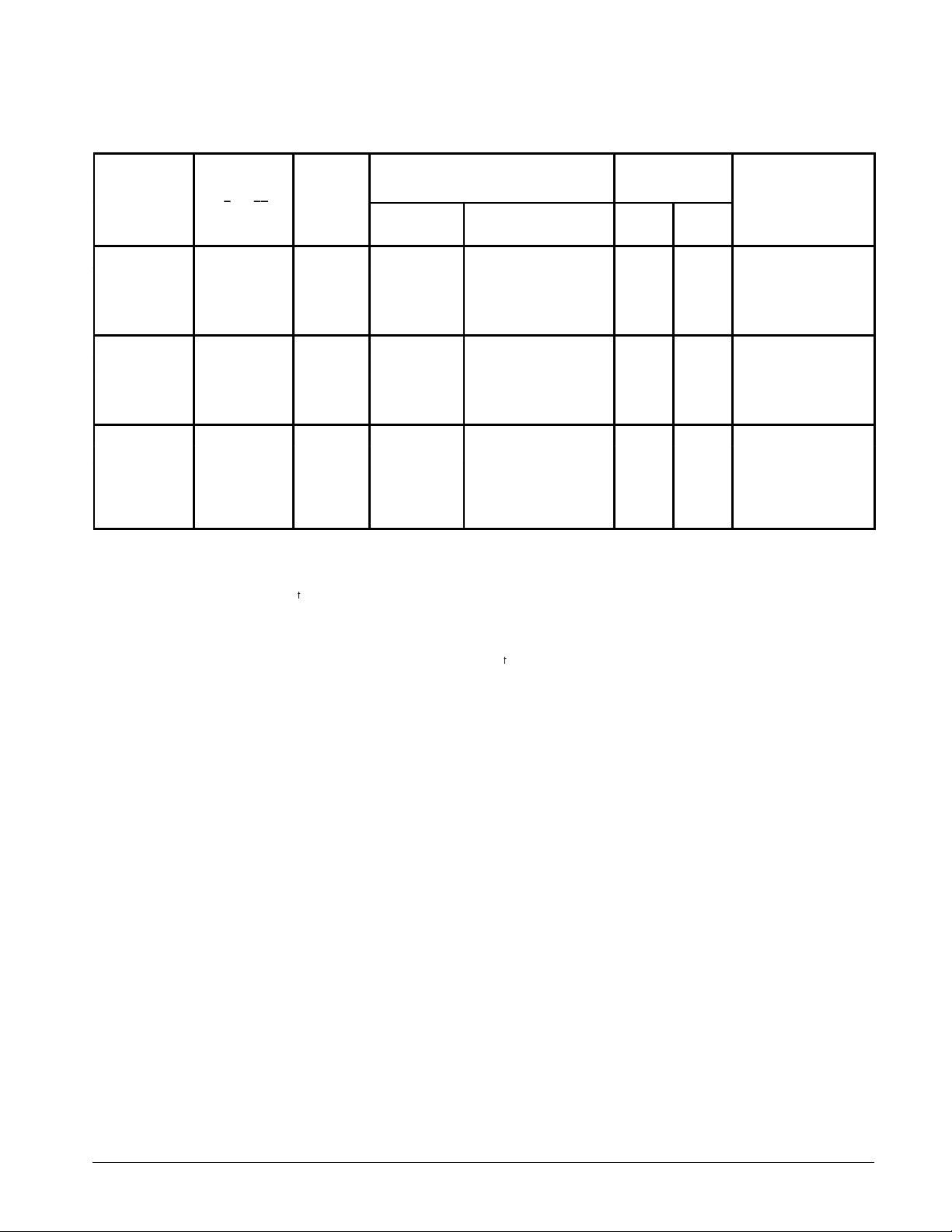
GENERAL DATA — 500 mW DO-35 GLASS
T
V
C
t
I
ype
Number
(Note 1)
Nominal
Zener Voltage
Z
(Note 2)
Volts
Test
urren
I
ZT
mA
Maximum Zener Impedance
(Note 3)
ZZT @ I
Ohms
ZT
ZZK @ I
Ohms
ZK
I
ZK
mA
Maximum
DC Zener Current
ZM
(Note 4)
mA
Maximum Reverse Leakage Current
IR MaximumµATest Voltage Vdc
1N981B 68 1.8 230 2000 0.25 4.5 5 51.7
1N982B 75 1.7 270 2000 0.25 4.1 5 56
1N983B 82 1.5 330 3000 0.25 3.7 5 62.2
1N984B 91 1.4 400 3000 0.25 3.3 5 69.2
1N985B 100 1.3 500 3000 0.25 3 5 76
1N986B 110 1.1 750 4000 0.25 2.7 5 83.6
1N987B 120 1 900 4500 0.25 2.5 5 91.2
1N988B 130 0.95 1100 5000 0.25 2.3 5 98.8
1N989B 150 0.85 1500 6000 0.25 2 5 114
1N990B 160 0.8 1700 6500 0.25 1.9 5 121.6
1N991B 180 0.68 2200 7100 0.25 1.7 5 136.8
1N992B 200 0.65 2500 8000 0.25 1.5 5 152
NOTE 1. TOLERANCE AND VOLTAGE DESIGNATION
Tolerance Designation
The type numbers shown have tolerance designations as follows:
1N4370A series: ±5% units, C for ±2%, D for ±1%.
1N746A series: ±5% units, C for ±2%, D for ±1%.
1N957B series: ±5% units, C for ±2%, D for ±1%.
NOTE 2. ZENER VOLTAGE (VZ) MEASUREMENT
Nominal zener voltage is measured with the device junction in thermal equilibrium at the lead
temperature of 30°C ±1°C and 3/8″ lead length.
NOTE 3. ZENER IMPEDANCE (ZZ) DERIVATION
ZZT and ZZK are measured by dividing the ac voltage drop across the device by the ac current
applied. The specified limits are for IZ(ac) = 0.1 IZ(dc) with the ac frequency = 60 Hz.
NOTE 4. MAXIMUM ZENER CURRENT RATINGS (IZM)
Values shown are based on the JEDEC rating of 400 mW. Where the actual zener voltage
(VZ) is known at the operating point, the maximum zener current may be increased and is
limited by the derating curve.
V
R
500 mW DO-35 Glass Data Sheet
6-104
Motorola TVS/Zener Device Data
Page 9

GENERAL DATA — 500 mW DO-35 GLASS
Number
I
ZM
mA
∆V
Z
Volts
Low level oxide passivated zener diodes for applications re-
quiring extremely low operating currents, low leakage, and
• Zener Voltage Specified @ I
• Maximum Delta V
Given from 10 to 100 µA
Z
= 50 µA
ZT
sharp breakdown voltage.
ELECTRICAL CHARACTERISTICS
Zener Voltage
Type
Number
(Note 1)
Nom (Note 1) Min Max (Note 3)
1N4678 1.8 1.71 1.89 7.5 1 120 0.7
1N4679 2 1.9 2.1 5 1 110 0.7
1N4680 2.2 2.09 2.31 4 1 100 0.75
1N4681 2.4 2.28 2.52 2 1 95 0.8
1N4682 2.7 2.565 2.835 1 1 90 0.85
1N4683 3 2.85 3.15 0.8 1 85 0.9
1N4684 3.3 3.135 3.465 7.5 1.5 80 0.95
1N4685 3.6 3.42 3.78 7.5 2 75 0.95
1N4686 3.9 3.705 4.095 5 2 70 0.97
1N4687 4.3 4.085 4.515 4 2 65 0.99
1N4688 4.7 4.465 4.935 10 3 60 0.99
1N4689 5.1 4.845 5.355 10 3 55 0.97
1N4690 5.6 5.32 5.88 10 4 50 0.96
1N4691 6.2 5.89 6.51 10 5 45 0.95
1N4692 6.8 6.46 7.14 10 5.1 35 0.9
1N4693 7.5 7.125 7.875 10 5.7 31.8 0.75
1N4694 8.2 7.79 8.61 1 6.2 29 0.5
1N4695 8.7 8.265 9.135 1 6.6 27.4 0.1
1N4696 9.1 8.645 9.555 1 6.9 26.2 0.08
1N4697 10 9.5 10.5 1 7.6 24.8 0.1
1N4698 11 10.45 11.55 0.05 8.4 21.6 0.11
1N4699 12 11.4 12.6 0.05 9.1 20.4 0.12
1N4700 13 12.35 13.65 0.05 9.8 19 0.13
1N4701 14 13.3 14.7 0.05 10.6 17.5 0.14
1N4702 15 14.25 15.75 0.05 11.4 16.3 0.15
1N4703 16 15.2 16.8 0.05 12.1 15.4 0.16
1N4704 17 16.15 17.85 0.05 12.9 14.5 0.17
1N4705 18 17.1 18.9 0.05 13.6 13.2 0.18
1N4706 19 18.05 19.95 0.05 14.4 12.5 0.19
1N4707 20 19 21 0.01 15.2 11.9 0.2
1N4708 22 20.9 23.1 0.01 16.7 10.8 0.22
1N4709 24 22.8 25.2 0.01 18.2 9.9 0.24
1N4710 25 23.75 26.25 0.01 19 9.5 0.25
1N4711 27 25.65 28.35 0.01 20.4 8.8 0.27
1N4712 28 26.6 29.4 0.01 21.2 8.5 0.28
1N4713 30 28.5 31.5 0.01 22.8 7.9 0.3
1N4714 33 31.35 34.65 0.01 25 7.2 0.33
1N4715 36 34.2 37.8 0.01 27.3 6.6 0.36
1N4716 39 37.05 40.95 0.01 29.6 6.1 0.39
1N4717 43 40.85 45.15 0.01 32.6 5.5 0.43
VZ @ IZT = 50 µA
(TA = 25°C, VF = 1.5 V Max at IF = 100 mA for all types)
Maximum
Reverse Current
Volts
IR µA
Test
Voltage
VR Volts
Maximum
Zener Current
I
mA
(Note 2)
Maximum
Voltage Change
∆V
Volts
(Note 4)
NOTE 1. TOLERANCE AND VOLTAGE DESIGNATION (VZ)
The type numbers shown have a standard tolerance of ±5% on the nominal Zener voltage,
C for ±2%, D for ±1%.
NOTE 2. MAXIMUM ZENER CURRENT RATINGS (IZM)
Maximum Zener current ratings are based on maximum Zener voltage of the individual units
and JEDEC 250 mW rating.
NOTE 3. REVERSE LEAKAGE CURRENT (IR)
Motorola TVS/Zener Device Data
Reverse leakage currents are guaranteed and measured at VR as shown on the table.
NOTE 4. MAXIMUM VOLTAGE CHANGE (∆VZ)
Voltage change is equal to the difference between VZ at 100 µA and VZ at 10 µA.
NOTE 5. ZENER VOLTAGE (VZ) MEASUREMENT
Nominal Zener voltage is measured with the device junction in thermal equilibrium at the lead
temperature at 30°C ±1°C and 3/8″ lead length.
500 mW DO-35 Glass Data Sheet
6-105
Page 10
GENERAL DATA — 500 mW DO-35 GLASS
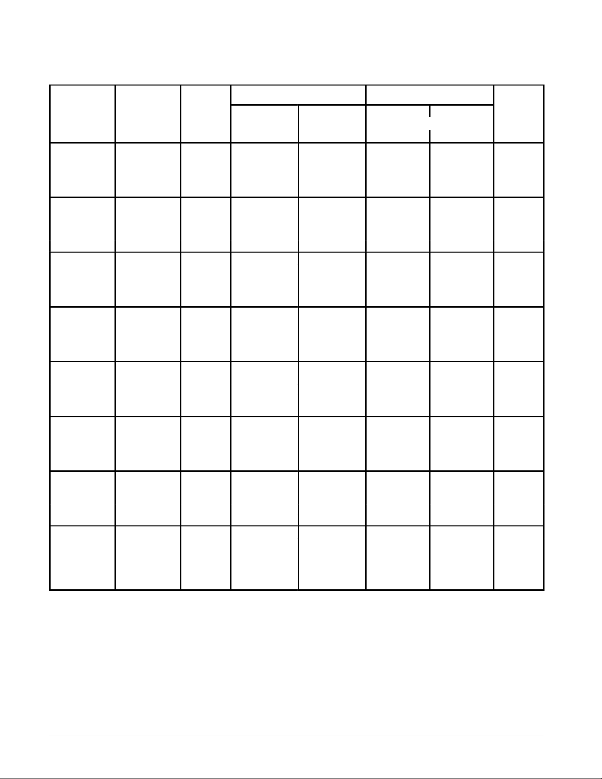
JEDEC
V
I
C
t
T
ELECTRICAL CHARACTERISTICS
= 3/8″; thermal resistance of heat sink = 30°C/W) VF = 1.1 Max @ IF = 200 mA for all types.
Nominal
Zener Voltage
@
Z
Type No.
(Note 1)
1N5221B 2.4 20 30 1200 100 1 –0.085
1N5222B 2.5 20 30 1250 100 1 –0.085
1N5223B 2.7 20 30 1300 75 1 –0.08
1N5224B 2.8 20 30 1400 75 1 –0.08
1N5225B 3 20 29 1600 50 1 –0.075
Volts
(Note 3)
ZT
(TA = 25°C unless otherwise noted. Based on dc measurements at thermal equilibrium; lead length
Test
urren
I
ZT
mA
Max Zener Impedance
ZZT@I
ZT
Ohms
(Note 4)
ZZK@IZK= 0.25 mA
Ohms
Max Reverse
Leakage Current
I
µA
R
V
R
Volts
Max Zener Voltage
emperature Coeff.
1N5226B 3.3 20 28 1600 25 1 –0.07
1N5227B 3.6 20 24 1700 15 1 –0.065
1N5228B 3.9 20 23 1900 10 1 –0.06
1N5229B 4.3 20 22 2000 5 1 ±0.055
1N5230B 4.7 20 19 1900 5 2 ±0.03
1N5231B 5.1 20 17 1600 5 2
1N5232B 5.6 20 11 1600 5 3 +0.038
1N5233B 6 20 7 1600 5 3.5 +0.038
1N5234B 6.2 20 7 1000 5 4 +0.045
1N5235B 6.8 20 5 750 3 5 +0.05
1N5236B 7.5 20 6 500 3 6 +0.058
1N5237B 8.2 20 8 500 3 6.5 +0.062
1N5238B 8.7 20 8 600 3 6.5 +0.065
1N5239B 9.1 20 10 600 3 7 +0.068
1N5240B 10 20 17 600 3 8 +0.075
1N5241B 11 20 22 600 2 8.4 +0.076
1N5242B 12 20 30 600 1 9.1 +0.077
1N5243B 13 9.5 13 600 0.5 9.9 +0.079
1N5244B 14 9 15 600 0.1 10 +0.082
1N5245B 15 8.5 16 600 0.1 11 +0.082
1N5246B 16 7.8 17 600 0.1 12 +0.083
1N5247B 17 7.4 19 600 0.1 13 +0.084
1N5248B 18 7 21 600 0.1 14 +0.085
1N5249B 19 6.6 23 600 0.1 14 +0.086
1N5250B 20 6.2 25 600 0.1 15 +0.086
1N5251B 22 5.6 29 600 0.1 17 +0.087
1N5252B 24 5.2 33 600 0.1 18 +0.088
1N5253B 25 5 35 600 0.1 19 +0.089
1N5254B 27 4.6 41 600 0.1 21 +0.09
1N5255B 28 4.5 44 600 0.1 21 +0.091
1N5256B 30 4.2 49 600 0.1 23 +0.091
1N5257B 33 3.8 58 700 0.1 25 +0.092
1N5258B 36 3.4 70 700 0.1 27 +0.093
1N5259B 39 3.2 80 800 0.1 30 +0.094
1N5260B 43 3 93 900 0.1 33 +0.095
1N5261B 47 2.7 105 1000 0.1 36 +0.095
1N5262B 51 2.5 125 1100 0.1 39 +0.096
1N5263B 56 2.2 150 1300 0.1 43 +0.096
1N5264B 60 2.1 170 1400 0.1 46 +0.097
1N5265B 62 2 185 1400 0.1 47 +0.097
θVZ (%/°C)
(Note 2)
±
0.03
(continued)
500 mW DO-35 Glass Data Sheet
6-106
Motorola TVS/Zener Device Data
Page 11
GENERAL DATA — 500 mW DO-35 GLASS
JEDEC
V
I
C
t
T
ELECTRICAL CHARACTERISTICS — continued
(TA = 25°C unless otherwise noted. Based on dc measurements at thermal equi-
librium; lead length = 3/8″; thermal resistance of heat sink = 30°C/W) VF = 1.1 Max @ IF = 200 mA for all types.
Type No.
(Note 1)
Nominal
Zener Voltage
@
Z
ZT
Volts
(Note 3)
Test
urren
I
ZT
mA
Max Zener Impedance
ZZT@I
ZT
Ohms
(Note 4)
ZZK@IZK= 0.25 mA
Ohms
Max Reverse
Leakage Current
µA
I
R
V
R
Volts
Max Zener Voltage
emperature Coeff.
1N5266B 68 1.8 230 1600 0.1 52 +0.097
1N5267B 75 1.7 270 1700 0.1 56 +0.098
1N5268B 82 1.5 330 2000 0.1 62 +0.098
1N5269B 87 1.4 370 2200 0.1 68 +0.099
1N5270B 91 1.4 400 2300 0.1 69 +0.099
1N5271B 100 1.3 500 2600 0.1 76 +0.1 1
1N5272B 110 1.1 750 3000 0.1 84 +0.11
1N5273B 120 1 900 4000 0.1 91 +0.11
1N5274B 130 0.95 1100 4500 0.1 99 +0.11
1N5275B 140 0.9 1300 4500 0.1 106 +0.11
1N5276B 150 0.85 1500 5000 0.1 114 +0.11
1N5277B 160 0.8 1700 5500 0.1 122 +0.11
1N5278B 170 0.74 1900 5500 0.1 129 +0.11
1N5279B 180 0.68 2200 6000 0.1 137 +0.11
1N5280B 190 0.66 2400 6500 0.1 144 +0.11
1N5281B 200 0.65 2500 7000 0.1 152 +0.11
NOTE 1. TOLERANCE
The JEDEC type numbers shown indicate a tolerance of ±5%. For tighter tolerance devices
use suffixes “C” for ±2% and “D” for ±1%.
NOTE 2. TEMPERATURE COEFFICIENT (θVZ)
Test conditions for temperature coefficient are as follows:
a. IZT = 7.5 mA, T1 = 25°C,
a. T2 = 125°C (1N5221B through 1N5242B).
b. IZT = Rated IZT, T1 = 25°C,
a. T2 = 125°C (1N5243B through 1N5281B).
Device to be temperature stabilized with current applied prior to reading breakdown voltage
at the specified ambient temperature.
NOTE 3. ZENER VOLTAGE (VZ) MEASUREMENT
Nominal zener voltage is measured with the device junction in thermal equilibrium at the lead
temperature of 30°C ±1°C and 3/8″ lead length.
NOTE 4. ZENER IMPEDANCE (ZZ) DERIVATION
ZZT and ZZK are measured by dividing the ac voltage drop across the device by the ac current
applied. The specified limits are for IZ(ac) = 0.1 IZ(dc) with the ac frequency = 60 Hz.
For more information on special selections contact your nearest Motorola representative.
θVZ (%/°C)
(Note 2)
Motorola TVS/Zener Device Data
500 mW DO-35 Glass Data Sheet
6-107
Page 12
GENERAL DATA — 500 mW DO-35 GLASS
*ELECTRICAL CHARACTERISTICS
Motorola
Type
Number
(Note 1)
Nominal
Zener Voltage
VZ @ I
ZT
Volts
(Note 4)
(TL = 30°C unless otherwise noted.) (VF = 1.5 Volts Max @ IF = 100 mAdc for all types.)
Max Zener Impedance (Note 3) Max Reverse Leakage Current
Test
Current
I
ZT
mA
ZZT@I
Ohms
ZT
ZZK@IZK =
Ohms 0.25 mA
I
µA
R
@
V
R
Volts
1N5985B 2.4 5 100 1800 100 1 208
1N5986B 2.7 5 100 1900 75 1 185
1N5987B 3 5 95 2000 50 1 167
1N5988B 3.3 5 95 2200 25 1 152
1N5989B 3.6 5 90 2300 15 1 139
1N5990B 3.9 5 90 2400 10 1 128
1N5991B 4.3 5 88 2500 5 1 116
1N5992B 4.7 5 70 2200 3 1.5 106
1N5993B 5.1 5 50 2050 2 2 98
1N5994B 5.6 5 25 1800 2 3 89
1N5995B 6.2 5 10 1300 1 4 81
1N5996B 6.8 5 8 750 1 5.2 74
1N5997B 7.5 5 7 600 0.5 6 67
1N5998B 8.2 5 7 600 0.5 6.5 61
1N5999B 9.1 5 10 600 0.1 7 55
1N6000B 10 5 15 600 0.1 8 50
1N6001B 11 5 18 600 0.1 8.4 45
1N6002B 12 5 22 600 0.1 9.1 42
1N6003B 13 5 25 600 0.1 9.9 38
1N6004B 15 5 32 600 0.1 11 33
1N6005B 16 5 36 600 0.1 12 31
1N6006B 18 5 42 600 0.1 14 28
1N6007B 20 5 48 600 0.1 15 25
1N6008B 22 5 55 600 0.1 17 23
1N6009B 24 5 62 600 0.1 18 21
1N6010B 27 5 70 600 0.1 21 19
1N6011B 30 5 78 600 0.1 23 17
1N6012B 33 5 88 700 0.1 25 15
1N6013B 36 5 95 700 0.1 27 14
1N6014B 39 2 130 800 0.1 30 13
1N6015B 43 2 150 900 0.1 33 12
1N6016B 47 2 170 1000 0.1 36 11
1N6017B 51 2 180 1300 0.1 39 9.8
1N6018B 56 2 200 1400 0.1 43 8.9
1N6019B 62 2 225 1400 0.1 47 8
1N6020B 68 2 240 1600 0.1 52 7.4
1N6021B 75 2 265 1700 0.1 56 6.7
1N6022B 82 2 280 2000 0.1 62 6.1
1N6023B 91 2 300 2300 0.1 69 5.5
1N6024B 100 1 500 2600 0.1 76 5
1N6025B 110 1 650 3000 0.1 84 4.5
*Indicates JEDEC Registered Data
NOTE 1. TOLERANCE AND VOLTAGE DESIGNATION
Tolerance designation — Device tolerances of ±5% are indicated by a “B” suffix, ±2% by a
“C” suffix, ±1% by a “D” suffix.
NOTE 2.
This data was calculated using nominal voltages. The maximum current handling capability
on a worst case basis is limited by the actual zener voltage at the operating point and the power derating curve.
NOTE 3.
ZZT and ZZK are measured by dividing the ac voltage drop across the device by the ac current
applied. The specified limits are for IZ(ac) = 0.1 IZ(dc) with the ac frequency = 1.0 kHz.
NOTE 4.
Nominal Zener Voltage (VZ) is measured with the device junction in thermal equilibrium at the
lead temperature of 30°C ±1°C and 3/8″ lead length.
Max DC
Zener
Current
I
ZM
(Note 2)
500 mW DO-35 Glass Data Sheet
6-108
Motorola TVS/Zener Device Data
Page 13

GENERAL DATA — 500 mW DO-35 GLASS
(Note 3)
ELECTRICAL CHARACTERISTICS
(TL = 30°C unless otherwise noted.) (VF = 1.3 Volts Max, IF = 100 mAdc for all types.)
Max Reverse
Leakage Current
IR at V
R
(µA)
T
amb
25°C
125°C
Max
T
amb
Max
V
(V)
R
Motorola
Type
Number
VZT at I
Min
(Note 1)
(V)
ZT
Max
(Note 1)
Max Zener
Impedance
Note 3
ZZT @ I
ZT
(Ohms)
Max
I
ZT
(mA)
BZX55C2V4RL 2.28 2.56 85 5 50 100 1 155
BZX55C2V7RL 2.5 2.9 85 5 10 50 1 135
BZX55C3V0RL 2.8 3.2 85 5 4 40 1 125
BZX55C3V3RL 3.1 3.5 85 5 2 40 1 115
BZX55C3V6RL 3.4 3.8 85 5 2 40 1 105
BZX55C3V9RL 3.7 4.1 85 5 2 40 1 95
BZX55C4V3RL 4 4.6 75 5 1 20 1 90
BZX55C4V7RL 4.4 5 60 5 0.5 10 1 85
BZX55C5V1RL 4.8 5.4 35 5 0.1 2 1 80
BZX55C5V6RL 5.2 6 25 5 0.1 2 1 70
BZX55C6V2RL 5.8 6.6 10 5 0.1 2 2 64
BZX55C6V8RL 6.4 7.2 8 5 0.1 2 3 58
BZX55C7V5RL 7 7.9 7 5 0.1 2 5 53
BZX55C8V2RL 7.7 8.7 7 5 0.1 2 6 47
BZX55C9V1RL 8.5 9.6 10 5 0.1 2 7 43
BZX55C10RL 9.4 10.6 15 5 0.1 2 7.5 40
BZX55C11RL 10.4 11.6 20 5 0.1 2 8.5 36
BZX55C12RL 11.4 12.7 20 5 0.1 2 9 32
BZX55C13RL 12.4 14.1 26 5 0.1 2 10 29
BZX55C15RL 13.8 15.6 30 5 0.1 2 11 27
BZX55C16RL 15.3 17.1 40 5 0.1 2 12 24
BZX55C18RL 16.8 19.1 50 5 0.1 2 14 21
BZX55C20RL 18.8 21.1 55 5 0.1 2 15 20
BZX55C22RL 20.8 23.3 55 5 0.1 2 17 18
BZX55C24RL 22.8 25.6 80 5 0.1 2 18 16
BZX55C27RL 25.1 28.9 80 5 0.1 2 20 14
BZX55C30RL 28 32 80 5 0.1 2 22 13
BZX55C33RL 31 35 80 5 0.1 2 24 12
BZX55C36RL 34 38 80 5 0.1 2 27 11
BZX55C39RL 37 41 90 2.5 0.1 5 28 10
BZX55C43RL 40 46 90 2.5 0.1 5 32 9.2
BZX55C47RL 44 50 110 2.5 0.1 5 35 8.5
BZX55C51RL 48 54 125 2.5 0.1 10 38 7.8
BZX55C56RL 52 60 135 2.5 0.1 10 42 7
BZX55C62RL 58 66 150 2.5 0.1 10 47 6.4
BZX55C68RL 64 72 160 2.5 0.1 10 51 5.9
BZX55C75RL 70 80 170 2.5 0.1 10 56 5.3
BZX55C82RL 77 87 200 2.5 0.1 10 62 4.8
BZX55C91RL 85 96 250 1 0.1 10 69 4.3
I
ZM
(mA)
(Note 2)
NOTE 1. TOLERANCE AND VOLTAGE DESIGNATION
Tolerance designation — The type numbers listed have zener voltage min/max limits as
shown. Device tolerance of ±2% are indicated by a “B” instead of a “C”. Zener voltage is measured with the device junction in thermal equilibrium at the lead temperature of 30°C ±1°C
and 3/8″ lead length.
NOTE 2.
This data was calculated using nominal voltages. The maximum current handling capability
Motorola TVS/Zener Device Data
on a worst case basis is limited by the actual zener voltage at the operating point and the power derating curve.
NOTE 3.
ZZT and ZZK are measured by dividing the ac voltage drop across the device by the ac current
applied. The specified limtis are for IZ(ac) = 0.1 IZ(dc) with the ac frequency = 1.0 kHz.
500 mW DO-35 Glass Data Sheet
6-109
Page 14

GENERAL DATA — 500 mW DO-35 GLASS
(pF)
(pF)
*ELECTRICAL CHARACTERISTICS
Zener Voltage
Device Type
(Note 2)
Min Max
(TL = 30°C unless otherwise noted.) (VF = 1.5 Volts Max @ IF = 100 mAdc for all types.)
(Note 1)
(Note 4)
IZT=
(mA)
Impedance (Ohm)
@ I
ZT
f = 1000 Hz
Max
(Note 3)
Leakage Current
(µA)
@VR=
Max
(Volt)
Temp. Coefficient
(Typical)
(mV/°C)
Min Max
Capacitance
f = 1.0 MHz
BZX79C2V4RL 2.2 2.6 5 100 100 1 –3.5 0 255
BZX79C2V7RL 2.5 2.9 5 100 75 1 –3.5 0 230
BZX79C3V0RL 2.8 3.2 5 95 50 1 –3.5 0 215
BZX79C3V3RL 3.1 3.5 5 95 25 1 –3.5 0 200
BZX79C3V6RL 3.4 3.8 5 90 15 1 –3.5 0 185
BZX79C3V9RL 3.7 4.1 5 90 10 1 –3.5 +0.3 175
BZX79C4V3RL 4 4.6 5 90 5 1 –3.5 +1 160
BZX79C4V7RL 4.4 5 5 80 3 2 –3.5 +0.2 130
BZX79C5V1RL 4.8 5.4 5 60 2 2 –2.7 +1.2 110
BZX79C5V6RL 5.2 6 5 40 1 2 –2 +2.5 95
BZX79C6V2RL 5.8 6.6 5 10 3 4 0.4 3.7 90
BZX79C6V8RL 6.4 7.2 5 15 2 4 1.2 4.5 85
BZX79C7V5RL 7 7.9 5 15 1 5 2.5 5.3 80
BZX79C8V2RL 7.7 8.7 5 15 0.7 5 3.2 6.2 75
BZX79C9V1RL 8.5 9.6 5 15 0.5 6 3.8 7 70
BZX79C10RL 9.4 10.6 5 20 0.2 7 4.5 8 70
BZX79C11RL 10.4 11.6 5 20 0.1 8 5.4 9 65
BZX79C12RL 11.4 12.7 5 25 0.1 8 6 10 65
BZX79C13RL 12.4 14.1 5 30 0.1 8 7 11 60
BZX79C15RL 13.8 15.6 5 30 0.05 10.5 9.2 13 55
BZX79C16RL 15.3 17.1 5 40 0.05 11.2 10.4 14 52
BZX79C18RL 16.8 19.1 5 45 0.05 12.6 12.9 16 47
BZX79C20RL 18.8 21.2 5 55 0.05 14 14.4 18 36
BZX79C22RL 20.8 23.3 5 55 0.05 15.4 16.4 20 34
BZX79C24RL 22.8 25.6 5 70 0.05 16.8 18.4 22 33
BZX79C27RL 25.1 28.9 2 80 0.05 18.9 23.5 30
BZX79C30RL 28 32 2 80 0.05 21 26 27
BZX79C33RL 31 35 2 80 0.05 23.1 29 25
BZX79C36RL 34 38 2 90 0.05 25.2 31 23
BZX79C39RL 37 41 2 130 0.05 27.3 34 21
BZX79C43RL 40 46 2 150 0.05 30.1 37 21
BZX79C47RL 44 50 2 170 0.05 32.9 40 19
BZX79C51RL 48 54 2 180 0.05 35.7 44 19
BZX79C56RL 52 60 2 200 0.05 39.2 47 18
BZX79C62RL 58 66 2 215 0.05 43.4 51 17
BZX79C68RL 64 72 2 240 0.05 47.6 56 17
BZX79C75RL 70 79 2 255 0.05 52.5 60 16.5
BZX79C82RL 77 87 2 280 0.1 62 46 95 29
BZX79C91RL 85 96 2 300 0.1 69 51 107 28
BZX79C100RL 94 106 1 500 0.1 76 57 119 27
BZX79C110RL 104 116 1 650 0.1 84 63 131 26
BZX79C120RL 114 127 1 800 0.1 91 69 144 24
BZX79C130RL 124 141 1 950 0.1 99 75 158 23
BZX79C150RL 138 156 1 1250 0.1 114 87 185 21
BZX79C160RL 153 171 1 1400 0.1 122 93 200 20
BZX79C180RL 168 191 1 1700 0.1 137 105 228 18
BZX79C200RL 188 212 1 2000 0.1 152 120 255 17
(Typical)
VR = 0,
NOTE 1. Zener voltage is measured under pulse conditions such that TJ is no more than 2°C
above TA.
NOTE 2. TOLERANCE AND VOLTAGE DESIGNATION
Tolerance designation —– The type numbers listed have zener voltage min/max limits as
500 mW DO-35 Glass Data Sheet
6-110
shown. Device tolerances of ±2% are indicated by a “B” instead of a “C,” and ±1% by “A.”
NOTE 3. ZZT is measured by dividing the ac voltage drop across the device by the ac current
applied. The specified limits are for IZ(ac) = 0.1 IZ(dc) with the ac frequency = 1.0 kHz.
Motorola TVS/Zener Device Data
Page 15

GENERAL DATA — 500 mW DO-35 GLASS
yp p
at I
ZT
ELECTRICAL CHARACTERISTICS
Motorola ZPD and BZX83C series. Forward Voltage VF = 1 Volt Max at IF = 50 mA.
Device Type Nominal Min Max at I
BZX83C2V7RL ZPD2.7RL 2.7 2.5 2.9 85 600 500 –0.09...–0.04 1 — 100 mA
BZX83C3V0RL ZPD3.0RL 3 2.8 3.2 90 600 500 –0.09...–0.03 1 — 160 mA
BZX83C3V3RL ZPD3.3RL 3.3 3.1 3.5 90 600 500 –0.08...–0.03 1 — 130 mA
BZX83C3V6RL ZPD3.6RL 3.6 3.4 3.8 90 600 500 –0.08...–0.03 1 — 120 mA
BZX83C3V9RL ZPD3.9RL 3.9 3.7 4.1 85 600 500 –0.07...–0.03 1 — 110mA
BZX83C4V3RL ZPD4.3RL 4.3 4 4.6 80 600 500 –0.06...–0.01 1 — 115 mA
BZX83C4V7RL ZPD4.7RL 4.7 4.4 5 78 600 500 –0.05...+0.02 1 — 112 mA
BZX83C5V1RL ZPD5.1RL 5.1 4.8 5.4 60 550 480 –0.03...+0.04 0.8 100 nA
BZX83C5V6RL ZPD5.6RL 5.6 5.2 6 40 450 400 –0.02...+0.06 1 100 nA
BZX83C6V2RL ZPD6.2RL 6.2 5.8 6.6 10 200 –0.01...+0.07 2 100 nA
BZX83C6V8RL ZPD6.8RL 6.8 6.4 7.2 8 150 +0.02...+0.07 3 100 nA
BZX83C7V5RL ZPD7.5RL 7.5 7 7.9 7 50 +0.03...+0.07 5 100 nA
BZX83C8V2RL ZPD8.2RL 8.2 7.7 8.7 7 50 +0.04...+0.07 6 100 nA
BZX83C9V1RL ZPD9.1RL 9.1 8.5 9.6 10 50 +0.05...+0.08 7 100 nA
BZX83C10RL ZPD10RL 10 9.4 10.6 15 70 +0.05...+0.08 7.5 100 nA
BZX83C11RL ZPD11RL 11 10.4 11.6 20 70 +0.05...+0.09 8.5 100 nA
BZX83C12RL ZPD12RL 12 11.4 12.7 20 90 +0.06...+0.09 9 100 nA
BZX83C13RL ZPD13RL 13 12.4 14.1 25 110 +0.07...+0.09 10 100 nA
BZX83C15RL ZPD15RL 15 13.8 15.6 30 110 +0.07...+0.09 11 100 nA
BZX83C16RL ZPD16RL 16 15.3 17.1 40 170 +0.08...+0.095 12 100 nA
BZX83C18RL ZPD18RL 18 16.8 19.1 50 170 +0.08...+0.10 14 100 nA
BZX83C20RL ZPD20RL 20 18.8 21.2 55 220 +0.08...+0.10 15 100 nA
BZX83C22RL ZPD22RL 22 20.8 23.3 55 220 +0.08...+0.10 17 100 nA
BZX83C24RL ZPD24RL 24 22.8 25.6 80 220 +0.08...+0.10 18 100 nA
BZX83C27RL ZPD27RL 27 25.1 28.9 80 250 +0.08...+0.10 20 100 nA
BZX83C30RL ZPD30RL 30 28 32 80 250 +0.08...+0.10 22 100 nA
BZX83C33RL ZPD33RL 33 31 35 80 250 +0.08...+0.10 24 100 nA
NOTE 1. Pulse test.
NOTE 2. f = 1.0 kHz, IZ(ac) = 0.1 IZ(dc).
(at TA = 25°C)
Zener Voltage (Note 1)
at IZT= 5.0 mA
Impedance (Ω)
Max (Note 2)
at IZ = 1 mA
BZX83 ZPD
ZT
Typ. Temp.
Coeff.
at I
% per °C
VR Min
V
BZX83 ZPD at I
R
Motorola TVS/Zener Device Data
500 mW DO-35 Glass Data Sheet
6-111
Page 16

GENERAL DATA — 500 mW DO-35 GLASS
Designed for 250 mW applications requiring low leakage,
low impedance. Same as 1N4099 through 1N4104 and
1N4614 through 1N4627 except low noise test omitted.
ELECTRICAL CHARACTERISTICS (T
= 25°C unless otherwise specified. IZT = 250 µA and VF = 1 V Max @ IF = 200 mA for all
A
• Voltage Range from 1.8 to 10 Volts
• Zener Impedance and Zener Voltage Specified for Low-
Level Operation at IZT = 250 µA
ELECTRICAL CHARACTERISTICS types)
Nominal
Zener Voltage
Type
Number
(Note 1)
V
Z
(Note 2)
(Volts)
MZ4614 1.8 1200 7.5 1 120
MZ4615 2 1250 5 1 110
MZ4616 2.2 1300 4 1 100
MZ4617 2.4 1400 2 1 95
MZ4618 2.7 1500 1 1 90
MZ4619 3 1600 0.8 1 85
MZ4620 3.3 1650 7.5 1.5 80
MZ4621 3.6 1700 7.5 2 75
MZ4622 3.9 1650 5 2 70
MZ4623 4.3 1600 4 2 65
MZ4624 4.7 1550 10 3 60
MZ4625 5.1 1500 10 3 55
MZ4626 5.6 1400 10 4 50
MZ4627 6.2 1200 10 5 45
MZ4099 6.8 200 10 5.2 35
MZ4100 7.5 200 10 5.7 31.8
MZ4101 8.2 200 1 6.3 29
MZ4102 8.7 200 1 6.7 27.4
MZ4103 9.1 200 1 7 26.2
MZ4104 10 200 1 7.6 24.8
Max Zener
Impedance
Z
ZT
(Note 3)
(Ohms)
Max
Reverse
Current
I
R
(µA)
@
(Note 5)
Test
Voltage
V
R
(Volts)
Max Zener Current
I
ZM
(Note 4)
(mA)
NOTE 1. TOLERANCE AND VOLTAGE DESIGNATION
The type numbers shown have a standard tolerance of ±5% on the nominal zener voltage.
NOTE 2. ZENER VOLTAGE (VZ) MEASUREMENT
Nominal Zener Voltage is measured with the device junction in the thermal equilibrium with
ambient temperature of 25°C.
NOTE 3. ZENER IMPEDANCE (ZZT) DERIVATION
The zener impedance is derived from the 60 cycle ac voltage, which results when an ac current having an rms value equal to 10% of the dc zener current (IZT) is superimposed on IZT.
NOTE 4. MAXIMUM ZENER CURRENT RATINGS (IZM)
Maximum zener current ratings are based on maximum zener voltage of the individual units.
NOTE 5. REVERSE LEAKAGE CURRENT I
Reverse leakage currents are guaranteed and are measured at VR as shown on the table.
NOTE 6. SPECIAL SELECTORS AVAILABLE INCLUDE:
A) Tighter voltage tolerances. Contact your nearest Motorola representative for more infor-
mation.
R
500 mW DO-35 Glass Data Sheet
6-112
Motorola TVS/Zener Device Data
Page 17

GENERAL DATA — 500 mW DO-35 GLASS
Z
DC Z
Low Voltage Avalanche Passivated
Silicon Oxide Zener Regulator Diodes
Same as 1N5520B through 1N5530B except low noise test
spec omitted.
• Low Maximum Regulation Factor
• Low Zener Impedance
• Low Leakage Current
ELECTRICAL CHARACTERISTICS (T
ELECTRICAL CHARACTERISTICS V
Nominal
ener
Voltage
Motorola
Type No.
(Note 1)
VZ @ I
Volts
(Note 2)
ZT
Current
mAdc
= 25°C unless otherwise specified. Based on dc measurements at thermal equilibrium;
A
= 1.1 Max @ IF = 200 mA for all types.)
F
Maximum
ener
Current
I
ZM
mAdc
(Note 5)
Test
I
ZT
Max Zener
Impedance
ZZT @ I
ZT
Ohms
(Note 3)
Max Reverse Leakage Current
I
R
µAdc
(Note 4)
VR – Volts
Regulation
Factor
∆V
Z
Volts
(Note 6)
MZ5520B 3.9 20 22 1 1 98 0.85 2.0
MZ5521B 4.3 20 18 3 1.5 88 0.75 2.0
MZ5522B 4.7 10 22 2 2 81 0.6 1.0
MZ5523B 5.1 5 26 2 2.5 75 0.65 0.25
MZ5524B 5.6 3 30 2 3.5 68 0.3 0.25
MZ5525B 6.2 1 30 1 5 61 0.2 0.01
MZ5526B 6.8 1 30 1 6.2 56 0.1 0.01
MZ5527B 7.5 1 35 0.5 6.8 51 0.05 0.01
MZ5528B 8.2 1 40 0.5 7.5 46 0.05 0.01
MZ5529B 9.1 1 45 0.1 8.2 42 0.05 0.01
MZ5530B 10 1 60 0.05 9.1 38 0.1 0.01
NOTE 1. TOLERANCE AND VOLTAGE DESIGNATION
The “B” suffix type numbers listed are ±5% tolerance of nominal VZ.
NOTE 2. ZENER VOLTAGE (VZ) MEASUREMENT
Nominal zener voltage is measured with the device junction in thermal equilibrium with ambient temperature of 25°C.
NOTE 3. ZENER IMPEDANCE (ZZ) DERIVATION
The zener impedance is derived from the 60 Hz ac voltage, which results when an ac current
having an rms value equal to 10% of the dc zener current (IZT) is superimposed on IZT.
NOTE 4. REVERSE LEAKAGE CURRENT I
Reverse leakage currents are guaranteed and are measured at VR as shown on the table.
R
NOTE 5. MAXIMUM REGULATOR CURRENT (IZM)
The maximum current shown is based on the maximum voltage of a ±5% type unit, therefore,
it applies only to the “B” suffix device. The actual IZM for any device may not exceed the value
of 400 milliwatts divided by the actual VZ of the device.
NOTE 6. MAXIMUM REGULATION FACTOR (∆VZ)
∆VZ is the maximum difference between VZ at IZT and VZ at IZL measured with the device
junction in thermal equilibrium.
NOTE 7. SPECIAL SELECTORS AVAILABLE INCLUDE:
A) Tighter voltage tolerances. Contact your nearest Motorola representative for more infor-
mation.
Low
V
Z
Current
I
ZL
mAdc
Motorola TVS/Zener Device Data
500 mW DO-35 Glass Data Sheet
6-113
Page 18

GENERAL DATA — 500 mW DO-35 GLASS
Zener Voltage Regulator Diodes — Axial Leaded
500 mW DO-35 Glass
NOTES:
1. PACKAGE CONTOUR OPTIONAL WITHIN A AND B
B
D
K
F
A
F
K
HEAT SLUGS, IF ANY, SHALL BE INCLUDED
WITHIN THIS CYLINDER, BUT NOT SUBJECT TO
THE MINIMUM LIMIT OF B.
2. LEAD DIAMETER NOT CONTROLLED IN ZONE F
TO ALLOW FOR FLASH, LEAD FINISH BUILDUP
AND MINOR IRREGULARITIES OTHER THAN
HEAT SLUGS.
3. POLARITY DENOTED BY CATHODE BAND.
4. DIMENSIONING AND TOLERANCING PER ANSI
Y14.5M, 1982.
MILLIMETERS INCHES
MIN MINMAX MAX
DIM
A
3.05
5.08
0.120
B
1.52
0.46
—
25.40
2.29
0.56
1.27
38.10
D
F
K
All JEDEC dimensions and notes apply.
0.060
0.018
—
1.000
0.200
0.090
0.022
0.050
1.500
CASE 299-02
DO-204AH
GLASS
(Refer to Section 10 for Surface Mount, Thermal Data and Footprint Information.)
MULTIPLE PACKAGE QUANTITY (MPQ)
REQUIREMENTS
Package Option
Tape and Reel 5K
Tape and Ammo T A, TA2
NOTES: 1. The “2” suffix refers to 26 mm tape spacing.
NOTES: 2. Radial Tape and Reel may be available. Please contact your Motorola
NOTES: 2. representative.
Refer to Section 10 for more information on Packaging Specifications.
Type No. Suffix
(1)
RL, RL2
(1)
MPQ (Units)
5K
500 mW DO-35 Glass Data Sheet
6-114
Motorola TVS/Zener Device Data
Page 19

GENERAL DATA — 500 mW DO-35 GLASS
1–1.3 Watt DO-41 Glass
Zener Voltage Regulator Diodes
GENERAL DATA APPLICABLE TO ALL SERIES IN
THIS GROUP
One Watt Hermetically Sealed Glass
Silicon Zener Diodes
Specification Features:
• Complete Voltage Range — 3.3 to 100 Volts
• DO-41 Package
• Double Slug Type Construction
• Metallurgically Bonded Construction
• Oxide Passivated Die
Mechanical Characteristics:
CASE: Double slug type, hermetically sealed glass
MAXIMUM LEAD TEMPERATURE FOR SOLDERING PURPOSES: 230°C, 1/16″ from
case for 10 seconds
FINISH: All external surfaces are corrosion resistant with readily solderable leads
POLARITY: Cathode indicated by color band. When operated in zener mode, cathode
will be positive with respect to anode
MOUNTING POSITION: Any
WAFER FAB LOCATION: Phoenix, Arizona
ASSEMBLY/TEST LOCATION: Seoul, Korea
GENERAL
DATA
1–1.3 WATT
DO-41 GLASS
1 WATT
ZENER REGULATOR
DIODES
3.3–100 VOL TS
CASE 59-03
DO-41
GLASS
MAXIMUM RATINGS
Rating Symbol Value Unit
DC Power Dissipation @ TA = 50°C
Derate above 50°C
Operating and Storage Junction Temperature Range TJ, T
1.25
L = 1
1
0.75
0.5
0.25
D
P , MAXIMUM DISSIP ATION (WATTS)
0 20 40 60 20080 100 120 140 160 180
Figure 1. Power Temperature Derating Curve
TL, LEAD TEMPERATURE (°C)
L = 1/8
L = 3/8
L = LEAD LENGTH
″
TO HEAT SINK
″
″
P
D
stg
1
6.67
– 65 to +200 °C
Watt
mW/°C
Motorola TVS/Zener Device Data
500 mW DO-35 Glass Data Sheet
6-115
Page 20

GENERAL DATA — 500 mW DO-35 GLASS
a. Range for Units to 12 Volts b. Range for Units to 12 to 100 Volts
C)
+12
°
+10
+8
+6
+4
+2
0
, TEMPERATURE COEFFICIENT (mV/
–2
Z
V
θ
–4
23456789101112
V
, ZENER VOLTAGE (VOLTS)
Z
RANGE
(–55°C to +150°C temperature range; 90% of the units are in the ranges indicated.)
C/W)
°
175
150
125
100
VZ@I
ZT
Figure 2. T emperature Coefficients
100
C)
°
70
50
30
20
10
7
5
3
2
, TEMPERATURE COEFFICIENT (mV/
Z
V
θ
1
10 20 30 50 70 100
+6
C)
°
+4
+2
VZ@I
TA=25
RANGE VZ@I
VZ, ZENER VOLTAGE (VOLTS)
Z
°
C
20 mA
ZT
75
50
25
0
, JUNCTION-TO-LEAD THERMAL RESISTANCE (mV/
0 0.1 0.2 0.3 0.4 0.5 0.6 0.7 0.8 0.9 1
JL
θ
L, LEAD LENGTH TO HEA T SINK (INCHES)
Figure 3. T ypical Thermal Resistance
0
–2
, TEMPERATURE COEFFICIENT (mV/
Z
V
θ
–4
34 5678
NOTE: BELOW 3 VOLTS AND ABOVE 8 VOLTS
NOTE: CHANGES IN ZENER CURRENT DO NOT
NOTE: EFFECT TEMPERATURE COEFFICIENTS
1mA
V
, ZENER VOLTAGE (VOLTS)
Z
0.01 mA
Figure 4. Effect of Zener Current
versus Lead Length
100
70
50
30
20
10
7
5
3
, PEAK SURGE POWER (WATTS)
2
pk
P
1
0.01 0.02 0.05 0.1 0.2 0.5 1 2 5 10 20 50 100 200 500 1000
This graph represents 90 percentile data points.
For worst case design characteristics, multiply surge power by 2/3.
5% DUTY CYCLE
10% DUTY CYCLE
20% DUTY CYCLE
11V–100 V NONREPETITIVE
3.3 V–10 V NONREPETITIVE
PW, PULSE WIDTH (ms)
RECTANGULAR
WAVEFORM
°
C PRIOR TO
TJ=25
INITIAL PULSE
500 mW DO-35 Glass Data Sheet
6-1 16
Figure 5. Maximum Surge Power
Motorola TVS/Zener Device Data
Page 21

GENERAL DATA — 500 mW DO-35 GLASS
1000
500
200
100
50
20
10
5
, DYNAMIC IMPEDANCE (OHMS)
Z
Z
2
1
0.1 0.2 0.5 1 2 5 10 20 50 100
VZ = 2.7 V
47 V
27 V
6.2 V
IZ, ZENER CURRENT (mA)
TJ = 25°C
iZ(rms) = 0.1 IZ(dc)
f = 60 Hz
Figure 6. Effect of Zener Current
on Zener Impedance
10000
7000
5000
2000
1000
700
500
TYPICAL LEAKAGE CURRENT
AT 80% OF NOMINAL
BREAKDOWN VOLTAGE
1000
700
500
200
100
, DYNAMIC IMPEDANCE (OHMS)
Z
Z
IZ = 1 mA
70
50
20
10
7
5
2
1
1 2 100
5 mA
20 mA
35710 20305070
VZ, ZENER CURRENT (mA)
TJ = 25°C
iZ(rms) = 0.1 IZ(dc)
f = 60 Hz
Figure 7. Effect of Zener V oltage
on Zener Impedance
400
300
200
100
50
0 V BIAS
1 V BIAS
200
100
70
50
A)
20
µ
10
7
5
2
1
0.7
, LEAKAGE CURRENT (
0.5
R
I
0.2
0.1
0.07
0.05
0.02
0.01
0.007
0.005
0.002
0.001
3456789101112131415
V
, NOMINAL ZENER VOLTAGE (VOLTS)
Z
+125°C
+25°C
20
C, CAPACITANCE (pF)
10
8
4
1 2 5 10 20 50 100
50% OF BREAKDOWN BIAS
VZ, NOMINAL VZ (VOLTS)
Figure 9. T ypical Capacitance versus V
1000
500
200
100
50
20
10
, FORWARD CURRENT (mA)
5
150°C
F
I
2
1
0.4 0.5 0.6 0.7 0.8 0.9 1 1.1
MINIMUM
MAXIMUM
75°C
25°C
0°C
VF, FORWARD VOLTAGE (VOLTS)
Z
Figure 8. T ypical Leakage Current
Motorola TVS/Zener Device Data
Figure 10. T ypical Forward Characteristics
500 mW DO-35 Glass Data Sheet
6-117
Page 22

GENERAL DATA — 500 mW DO-35 GLASS
APPLICATION NOTE
Since the actual voltage available from a given zener diode
is temperature dependent, it is necessary to determine junction temperature under any set of operating conditions in order
to calculate its value. The following procedure is recommended:
Lead Temperature, TL, should be determined from:
TL = θLAPD + TA.
θLA is the lead-to-ambient thermal resistance (°C/W) and PD is
the power dissipation. The value for θLA will vary and depends
on the device mounting method. θLA is generally 30 to 40°C/W
for the various clips and tie points in common use and for
printed circuit board wiring.
The temperature of the lead can also be measured using a
thermocouple placed on the lead as close as possible to the tie
point. The thermal mass connected to the tie point is normally
large enough so that it will not significantly respond to heat
surges generated in the diode as a result of pulsed operation
once steady-state conditions are achieved. Using the measured value of TL, the junction temperature may be determined by:
TJ = TL + ∆TJL.
∆TJL is the increase in junction temperature above the lead
temperature and may be found as follows:
∆TJL = θJLPD.
θJL may be determined from Figure 3 for dc power condi-
tions. For worst-case design, using expected limits of IZ, limits
of PD and the extremes of TJ(∆TJ) may be estimated. Changes
in voltage, VZ, can then be found from:
∆V = θVZ ∆TJ.
θVZ, the zener voltage temperature coefficient, is found from
Figure 2.
Under high power-pulse operation, the zener voltage will
vary with time and may also be affected significantly by the
zener resistance. For best regulation, keep current excursions
as low as possible.
Surge limitations are given in Figure 5. They are lower than
would be expected by considering only junction temperature,
as current crowding effects cause temperatures to be extremely high in small spots, resulting in device degradation
should the limits of Figure 5 be exceeded.
500 mW DO-35 Glass Data Sheet
6-118
Motorola TVS/Zener Device Data
Page 23

GENERAL DATA — 500 mW DO-35 GLASS
*ELECTRICAL CHARACTERISTICS
Nominal
JEDEC
Type No.
(Note 1)
Zener Voltage
VZ @ I
ZT
Volts
(Notes 2 and 3)
(TA = 25°C unless otherwise noted) VF = 1.2 V Max, IF = 200 mA for all types.
Maximum Zener Impedance (Note 4) Leakage Current
Test
Current
I
ZT
mA
ZZT@I
Ohms
ZT
ZZK@I
Ohms
ZK
I
ZK
mA
I
R
µA Max
V
R
Volts
1N4728A 3.3 76 10 400 1 100 1 1380
1N4729A 3.6 69 10 400 1 100 1 1260
1N4730A 3.9 64 9 400 1 50 1 1190
1N4731A 4.3 58 9 400 1 10 1 1070
1N4732A 4.7 53 8 500 1 10 1 970
1N4733A 5.1 49 7 550 1 10 1 890
1N4734A 5.6 45 5 600 1 10 2 810
1N4735A 6.2 41 2 700 1 10 3 730
1N4736A 6.8 37 3.5 700 1 10 4 660
1N4737A 7.5 34 4 700 0.5 10 5 605
1N4738A 8.2 31 4.5 700 0.5 10 6 550
1N4739A 9.1 28 5 700 0.5 10 7 500
1N4740A 10 25 7 700 0.25 10 7.6 454
1N4741A 11 23 8 700 0.25 5 8.4 414
1N4742A 12 21 9 700 0.25 5 9.1 380
1N4743A 13 19 10 700 0.25 5 9.9 344
1N4744A 15 17 14 700 0.25 5 11.4 304
1N4745A 16 15.5 16 700 0.25 5 12.2 285
1N4746A 18 14 20 750 0.25 5 13.7 250
1N4747A 20 12.5 22 750 0.25 5 15.2 225
1N4748A 22 1 1.5 23 750 0.25 5 16.7 205
1N4749A 24 10.5 25 750 0.25 5 18.2 190
1N4750A 27 9.5 35 750 0.25 5 20.6 170
1N4751A 30 8.5 40 1000 0.25 5 22.8 150
1N4752A 33 7.5 45 1000 0.25 5 25.1 135
1N4753A 36 7 50 1000 0.25 5 27.4 125
1N4754A 39 6.5 60 1000 0.25 5 29.7 115
1N4755A 43 6 70 1500 0.25 5 32.7 110
1N4756A 47 5.5 80 1500 0.25 5 35.8 95
1N4757A 51 5 95 1500 0.25 5 38.8 90
1N4758A 56 4.5 110 2000 0.25 5 42.6 80
1N4759A 62 4 125 2000 0.25 5 47.1 70
1N4760A 68 3.7 150 2000 0.25 5 51.7 65
1N4761A 75 3.3 175 2000 0.25 5 56 60
1N4762A 82 3 200 3000 0.25 5 62.2 55
1N4763A 91 2.8 250 3000 0.25 5 69.2 50
1N4764A 100 2.5 350 3000 0.25 5 76 45
*Indicates JEDEC Registered Data.
NOTE 1. TOLERANCE AND TYPE NUMBER DESIGNATION
The JEDEC type numbers listed have a standard tolerance on the nominal zener voltage of
±5%. C for ±2%, D for ±1%.
NOTE 2. SPECIALS AVAILABLE INCLUDE:
Nominal zener voltages between the voltages shown and tighter voltage tolerances.
For detailed information on price, availability, and delivery , contact your nearest Motorola rep-
resentative.
NOTE 3. ZENER VOLTAGE (VZ) MEASUREMENT
Motorola guarantees the zener voltage when measured at 90 seconds while maintaining the
lead temperature (TL) at 30°C ± 1°C, 3/8″ from the diode body.
NOTE 4. ZENER IMPEDANCE (ZZ) DERIVATION
The zener impedance is derived from the 60 cycle ac voltage, which results when an ac current having an rms value equal to 10% of the dc zener current (IZT or IZK) is superimposed
on IZT or IZK.
NOTE 5. SURGE CURRENT (ir) NON-REPETITIVE
The rating listed in the electrical characteristics table is maximum peak, non-repetitive, reverse surge current of 1/2 square wave or equivalent sine wave pulse of 1/120 second duration superimposed on the test current, IZT, per JEDEC registration; however, actual device
capability is as described in Figure 5 of the General Data — DO-41 Glass.
Surge Current @
TA = 25°C
ir – mA
(Note 5)
Motorola TVS/Zener Device Data
500 mW DO-35 Glass Data Sheet
6-1 19
Page 24

GENERAL DATA — 500 mW DO-35 GLASS
Type
V
Z
V
Z
I
ZT
Max
I
R
i
(mA)
ELECTRICAL CHARACTERISTICS
Zener Voltage
VZT (V)
(Notes 2 and 3)
T
e V
(Note 1)
Min
(TA = 25°C unless otherwise noted.) (VF = 1.2 V Max, IF = 200 mA for all types.)
V
Max
Test
Current
I
(mA)
Zener Impedance
ZZ (ohms)
(Note 4)
Max
at I
ZT
Max at I
Z
(mA) VR (V)
Leakage
Current
(µA)
I
Max
Current
TA = 25°C
(Note 5)
BZX85C3V3RL 3.1 3.5 80 20 400 1 1 60 1380
BZX85C3V6RL 3.4 3.8 60 15 500 1 1 30 1260
BZX85C3V9RL 3.7 4.1 60 15 500 1 1 5 1190
BZX85C4V3RL 4 4.6 50 13 500 1 1 3 1070
BZX85C4V7RL 4.4 5 45 13 600 1 1.5 3 970
BZX85C5V1RL 4.8 5.4 45 10 500 1 2 1 890
BZX85C5V6RL 5.2 6 45 7 400 1 2 1 810
BZX85C6V2RL 5.8 6.6 35 4 300 1 3 1 730
BZX85C6V8RL 6.4 7.2 35 3.5 300 1 4 1 660
BZX85C7V5RL 7 7.9 35 3 200 0.5 4.5 1 605
BZX85C8V2RL 7.7 8.7 25 5 200 0.5 5 1 550
BZX85C9V1RL 8.5 9.6 25 5 200 0.5 6.5 1 500
BZX85C10RL 9.4 10.6 25 7 200 0.5 7 0.5 454
BZX85C11RL 10.4 11.6 20 8 300 0.5 7.7 0.5 414
BZX85C12RL 11.4 12.7 20 9 350 0.5 8.4 0.5 380
BZX85C13RL 12.4 14.1 20 10 400 0.5 9.1 0.5 344
BZX85C15RL 13.8 15.6 15 15 500 0.5 10.5 0.5 304
BZX85C16RL 15.3 17.1 15 15 500 0.5 11 0.5 285
BZX85C18RL 16.8 19.1 15 20 500 0.5 12.5 0.5 250
BZX85C20RL 18.8 21.2 10 24 600 0.5 14 0.5 225
BZX85C22RL 20.8 23.3 10 25 600 0.5 15.5 0.5 205
BZX85C24RL 22.8 25.6 10 25 600 0.5 17 0.5 190
BZX85C27RL 25.1 28.9 8 30 750 0.25 19 0.5 170
BZX85C30RL 28 32 8 30 1000 0.25 21 0.5 150
BZX85C33RL 31 35 8 35 1000 0.25 23 0.5 135
BZX85C36RL 34 38 8 40 1000 0.25 25 0.5 125
BZX85C39RL 37 41 6 45 1000 0.25 27 0.5 115
BZX85C43RL 40 46 6 50 1000 0.25 30 0.5 110
BZX85C47RL 44 50 4 90 1500 0.25 33 0.5 95
BZX85C51RL 48 54 4 115 1500 0.25 36 0.5 90
BZX85C56RL 52 60 4 120 2000 0.25 39 0.5 80
BZX85C62RL 58 66 4 125 2000 0.25 43 0.5 70
BZX85C68RL 64 72 4 130 2000 0.25 47 0.5 65
BZX85C75RL 70 80 4 150 2000 0.25 51 0.5 60
BZX85C82RL 77 87 2.7 200 3000 0.25 56 0.5 55
BZX85C91RL 85 96 2.7 250 3000 0.25 62 0.5 50
BZX85C100RL 96 106 2.7 350 3000 0.25 68 0.5 45
Surge
r
NOTE 1. TOLERANCE AND TYPE NUMBER DESIGNATION
The type numbers listed have zener voltage min/max limits as shown. Device tolerance of
±2% are indicated by a “B” instead of “C.”
NOTE 2. SPECIALS AVAILABLE INCLUDE:
Nominal zener voltages between the voltages shown and tighter voltage tolerances.
For detailed information on price, availability, and delivery , contact your nearest Motorola rep-
resentative.
NOTE 3. ZENER VOLTAGE (VZ) MEASUREMENT
VZ is measured after the test current has been applied to 40 ± 10 msec., while maintaining
the lead temperature (TL) at 30°C ± 1°C, 3/8″ from the diode body.
500 mW DO-35 Glass Data Sheet
6-120
NOTE 4. ZENER IMPEDANCE (ZZ) DERIVATION
The zener impedance is derived from the 1 kHz cycle ac voltage, which results when an ac
current having an rms value equal to 10% of the dc zener current (IZT) or (IZK) is superimposed on IZT or IZK.
NOTE 5. SURGE CURRENT (ir) NON-REPETITIVE
The rating listed in the electrical characteristics table is maximum peak, non-repetitive, reverse surge current of 1/2 square wave or equivalent sine wave pulse of 1/120 second duration superimposed on the test current IZT. However, actual device capability is as described
in Figure 5 of General Data DO-41 glass.
Motorola TVS/Zener Device Data
Page 25

GENERAL DATA — 500 mW DO-35 GLASS
T
I
ELECTRICAL CHARACTERISTICS
(TA = 25°C unless otherwise noted) VF = 1.2 V Max, IF = 200 mA for all types.
Zener Impedance
Current
TA = 25°C
(Note 5)
ype No.
(Note 1)
Zener Voltage (V)
(Notes 2 and 3)
VZ Min VZ Max
Test Current
ZT
(mA)
(Note 4)
f = 1 kHz (ohms)
Blocking
Volt Min (V)
Typ Max IR = 1 µA
MZPY3.9RL 3.7 4.1 100 4 7 — 1190
MZPY4.3RL 4 4.6 100 4 7 — 1070
MZPY4.7RL 4.4 5 100 4 7 — 970
MZPY5.1RL 4.8 5.4 100 2 5 0.7 890
MZPY5.6RL 5.2 6 100 1 2 1.5 810
MZPY6.2RL 5.8 6.6 100 1 2 2 730
MZPY6.8RL 6.4 7.2 100 1 2 3 660
MZPY7.5RL 7 7.9 100 1 2 5 605
MZPY8.2RL 7.7 8.7 100 1 2 6 550
MZPY9.1RL 8.5 9.6 50 2 4 7 500
MZPY10RL 9.4 10.6 50 2 4 7.5 454
MZPY11RL 10.4 1 1.6 50 3 7 8.5 414
MZPY12RL 11.4 12.7 50 3 7 9 380
MZPY13RL 12.4 14.1 50 4 9 10 344
MZPY15RL 14.2 15.8 50 4 9 11 304
MZPY16RL 15.3 17.1 25 5 10 12 285
MZPY18RL 16.8 19.1 25 5 11 14 250
MZPY20RL 18.8 21.2 25 6 12 15 225
MZPY22RL 20.8 23.3 25 7 13 17 205
MZPY24RL 22.8 25.6 25 8 14 18 190
MZPY27RL 25.1 28.9 25 9 15 20 170
MZPY30RL 28 32 25 10 20 22.5 150
MZPY33RL 31 35 25 11 20 25 135
MZPY36RL 34 38 10 25 60 27 125
MZPY39RL 37 41 10 30 60 29 115
MZPY43RL 40 46 10 35 80 32 110
MZPY47RL 44 50 10 40 80 35 95
MZPY51RL 48 54 10 45 100 38 90
MZPY56RL 52 60 10 50 100 42 80
MZPY62RL 58 66 10 60 130 47 70
MZPY68RL 64 72 10 65 130 51 65
MZPY75RL 70 79 10 70 160 56 60
MZPY82RL 77 88 10 80 160 61 55
MZPY91RL 85 96 5 120 250 68 50
MZPY100RL 94 106 5 130 250 75 45
Surge
ir (ma)
NOTE 1. TOLERANCE AND TYPE NUMBER DESIGNATION
The type numbers listed have zener voltage min/max limits as shown. Device tolerance of
±2% are indicated by a “C” and ±1% by a “D” suffix.
NOTE 2. SPECIALS AVAILABLE INCLUDE:
Nominal zener voltages between the voltages shown and tighter voltage tolerances.
For detailed information on price, availability, and delivery , contact your nearest Motorola rep-
resentative.
NOTE 3. ZENER VOLTAGE (VZ) MEASUREMENT
VZ is measured after the test current has been applied to 40 ± 10 msec., while maintaining
the lead temperature (TL) at 30°C ± 1°C, 3/8″ from the diode body.
Motorola TVS/Zener Device Data
NOTE 4. ZENER IMPEDANCE (ZZ) DERIVATION
The zener impedance is derived from the 1 kHz cycle ac voltage, which results when an ac
current having an rms value equal to 10% of the dc zener current (IZT) of (IZK) is superimposed on IZT or IZK.
NOTE 5. SURGE CURRENT (ir) NON-REPETITIVE
The rating listed in the electrical characteristics table is maximum peak, non-repetitive, reverse surge current of 1/2 square wave or equivalent sine wave pulse of 1/120 second duration superimposed on the test current IZT, however, actual device capability is as described
in Figure 5 of General Data DO-41 glass.
500 mW DO-35 Glass Data Sheet
6-121
Page 26

GENERAL DATA — 500 mW DO-35 GLASS
Zener Voltage Regulator Diodes — Axial Leaded
1–1.3 Watt DO-41 Glass
B
NOTES:
1. ALL RULES AND NOTES ASSOCIATED WITH
JEDEC DO-41 OUTLINE SHALL APPLY.
K
D
F
A
F
K
2. POLARITY DENOTED BY CATHODE BAND.
3. LEAD DIAMETER NOT CONTROLLED WITHIN F
DIMENSION.
MILLIMETERS INCHES
MIN MINMAX MAX
DIM
A
4.07
5.20
0.160
B
2.04
0.71
—
27.94
2.71
0.86
1.27
—
D
F
K
0.080
0.028
—
1.100
0.205
0.107
0.034
0.050
—
CASE 59-03
DO-41
GLASS
(Refer to Section 10 for Surface Mount, Thermal Data and Footprint Information.)
MULTIPLE PACKAGE QUANTITY (MPQ)
REQUIREMENTS
Package Option
Tape and Reel 6K
Tape and Ammo T A, TA2 4K
NOTE: 1. The “2” suffix refers to 26 mm tape spacing.
(Refer to Section 10 for more information on Packaging Specifications.)
Type No. Suffix
RL, RL2
MPQ (Units)
500 mW DO-35 Glass Data Sheet
6-122
Motorola TVS/Zener Device Data
Page 27

GENERAL DATA — 500 mW DO-35 GLASS
1 to 3 Watt DO-41 Surmetic 30
Zener Voltage Regulator Diodes
GENERAL DATA APPLICABLE TO ALL SERIES IN
THIS GROUP
1 to 3 Watt Surmetic 30
Silicon Zener Diodes
...a complete series of 1 to 3 Watt Zener Diodes with limits and operating characteristics
that reflect the superior capabilities of silicon-oxide-passivated junctions. All this in an
axial-lead, transfer-molded plastic package offering protection in all common environmental conditions.
Specification Features:
• Surge Rating of 98 Watts @ 1 ms
• Maximum Limits Guaranteed On Up To Six Electrical Parameters
• Package No Larger Than the Conventional 1 Watt Package
Mechanical Characteristics:
CASE: Void-free, transfer-molded, thermosetting plastic
FINISH: All external surfaces are corrosion resistant and leads are readily solderable
POLARITY: Cathode indicated by color band. When operated in zener mode, cathode
will be positive with respect to anode
MOUNTING POSITION: Any
WEIGHT: 0.4 gram (approx)
WAFER FAB LOCATION: Phoenix, Arizona
ASSEMBLY/TEST LOCATION: Seoul, Korea
GENERAL
DATA
1–3 WATT
DO-41
SURMETIC 30
1 TO 3 WATT
ZENER REGULATOR
DIODES
3.3–400 VOL TS
CASE 59-03
DO-41
PLASTIC
MAXIMUM RATINGS
Rating Symbol Value Unit
DC Power Dissipation @ TL = 75°C
Lead Length = 3/8″
Derate above 75°C
DC Power Dissipation @ TA = 50°C
Derate above 50°C
Operating and Storage Junction Temperature Range TJ, T
5
L = 1/8
4
L = 3/8
3
2
L = 1
1
D
P , MAXIMUM DISSIP ATION (WATTS)
0
0 20 40 60 20080 100 120 140 160 180
″
″
TL, LEAD TEMPERATURE (°C)
″
L = LEAD LENGTH
TO HEAT SINK
P
D
P
D
stg
3
24
1
6.67
– 65 to +200 °C
Watts
mW/°C
Watt
mW/°C
Motorola TVS/Zener Device Data
Figure 1. Power Temperature Derating Curve
500 mW DO-35 Glass Data Sheet
6-123
Page 28

GENERAL DATA — 500 mW DO-35 GLASS
30
20
10
°
0.7
JUNCTION-TO-LEAD ( C/W)
0.5
(t, D) TRANSIENT THERMAL RESISTANCE
JL
θ
0.3
0.0001 0.0002 0.0005 0.001 0.002 0.005 0.01 0.02 0.05 0.1 0.2 0.5 1 2 5 10
D =0.5
7
5
3
2
1
0.2
0.1
0.05
0.02
0.01
D = 0
NOTE: BELOW 0.1 SECOND, THERMAL
RESPONSE CURVE IS APPLICABLE
TO ANY LEAD LENGTH (L).
t, TIME (SECONDS)
P
PK
DUTY CYCLE, D =t1/t
SINGLE PULSE ∆TJL =
REPETITIVE PULSES
θJL (t)P
∆
TJL =
t
1
t
2
PK
θJL (t,D)P
Figure 2. T ypical Thermal Response L, Lead Length = 3/8 Inch
2
PK
1K
500
300
200
100
50
30
PK
20
P , PEAK SURGE POWER (WATTS)
10
0.1 0.2 0.3 0.5 1 2 3 5 10 20 30 50 100
PW, PULSE WIDTH (ms)
RECTANGULAR
NONREPETITIVE
WAVEFORM
TJ=25
°
C PRIOR
TO INITIAL PULSE
Figure 3. Maximum Surge Power Figure 4. T ypical Reverse Leakage
APPLICATION NOTE
Since the actual voltage available from a given zener diode
is temperature dependent, it is necessary to determine junction temperature under any set of operating conditions in order
to calculate its value. The following procedure is recommended:
Lead Temperature, TL, should be determined from:
TL = θLA PD + T
θLA is the lead-to-ambient thermal resistance (°C/W) and
PD is the power dissipation. The value for θLA will vary and
depends on the device mounting method. θLA is generally
30–40°C/W for the various clips and tie points in common
use and for printed circuit board wiring.
The temperature of the lead can also be measured using a
thermocouple placed on the lead as close as possible to the tie
point. The thermal mass connected to the tie point is normally
large enough so that it will not significantly respond to heat
surges generated in the diode as a result of pulsed operation
once steady-state conditions are achieved. Using the measured value of TL, the junction temperature may be determined by:
TJ = TL + ∆T
A
JL
3
2
R
1
0.5
Adc) @ V
0.2
µ
0.1
0.05
0.02
0.01
0.005
0.002
, REVERSE LEAKAGE (
0.001
R
AS SPECIFIED IN ELEC. CHAR. T ABLE
I
0.0005
0.0003
1 2 5 10 20 50 100 200 400 1000
NOMINAL VZ (VOLTS)
TA = 125°C
TA = 125°C
∆TJL is the increase in junction temperature above the lead
temperature and may be found from Figure 2 for a train of
power pulses (L = 3/8 inch) or from Figure 10 for dc power.
∆TJL = θJL P
D
For worst-case design, using expected limits of IZ, limits of
PD and the extremes of TJ (∆TJ) may be estimated. Changes
in voltage, VZ, can then be found from:
∆V = θVZ ∆T
J
θVZ, the zener voltage temperature coefficient, is found from
Figures 5 and 6.
Under high power-pulse operation, the zener voltage will
vary with time and may also be affected significantly by the
zener resistance. For best regulation, keep current excursions
as low as possible.
Data of Figure 2 should not be used to compute surge capability. Surge limitations are given in Figure 3. They are lower
than would be expected by considering only junction temperature, as current crowding effects cause temperatures to be extremely high in small spots resulting in device degradation
should the limits of Figure 3 be exceeded.
500 mW DO-35 Glass Data Sheet
6-124
Motorola TVS/Zener Device Data
Page 29

°
ZTVZ
10
GENERAL DATA — 500 mW DO-35 GLASS
TEMPERATURE COEFFICIENT RANGES
(90% of the Units are in the Ranges Indicated)
1000
ZTVZ
8
500
°θ
6
4
2
0
–2
, TEMPERATURE COEFFICIENT (mV/ C) @ I
–4
θ
34 56789101112
VZ, ZENER VOLTAGE @ IZT (VOLTS)
RANGE
Figure 5. Units T o 12 Volts Figure 6. Units 10 T o 400 Volts
ZENER VOL TAGE versus ZENER CURRENT
(Figures 7, 8 and 9)
100
50
30
20
10
5
3
2
1
Z
I , ZENER CURRENT (mA)
0.5
0.3
0.2
0.1
012345678910
VZ, ZENER VOLTAGE (VOLTS)
Figure 7. VZ = 3.3 thru 10 Volts Figure 8. VZ = 12 thru 82 Volts
200
100
50
20
, TEMPERATURE COEFFICIENT (mV/ C) @ I
10
10 20 50 100 200 400 1000
VZ, ZENER VOLTAGE @ IZT (VOLTS)
100
50
30
20
10
5
3
2
1
Z
I , ZENER CURRENT (mA)
0.5
0.3
0.2
0.1
0 1020304050 60708090100
V
, ZENER VOLTAGE (VOLTS)
Z
10
5
2
1
0.5
Z
I , ZENER CURRENT (mA)
0.2
0.1
100 200 300 400250 350150
VZ, ZENER VOLTAGE (VOLTS)
Figure 9. VZ = 100 thru 400 V olts Figure 10. T ypical Thermal Resistance
Motorola TVS/Zener Device Data
80
°
( C/W)
70
60
50
40
30
T
20
10
0
0 1/8 1/4 3/8 1/2 5/8 3/4 7/8 1
, JUNCTION-TO-LEAD THERMAL RESISTANCE
JL
θ
L, LEAD LENGTH TO HEA T SINK (INCH)
PRIMARY PATH OF
CONDUCTION IS THROUGH
THE CATHODE LEAD
L
500 mW DO-35 Glass Data Sheet
LL
6-125
Page 30

GENERAL DATA — 500 mW DO-35 GLASS
T
V
@ I
C
t
C
*MAXIMUM RATINGS
Rating Symbol Value Unit
DC Power Dissipation @ TL = 75°C, Lead Length = 3/8″
Derate above 75°C
P
D
1.5
12
Watts
mW/°C
*ELECTRICAL CHARACTERISTICS (T
Motorola
ype
Number
(Note 1)
1N5913B 3.3 113.6 10 500 1 100 1 454
1N5914B 3.6 104.2 9 500 1 75 1 416
1N5915B 3.9 96.1 7.5 500 1 25 1 384
1N5916B 4.3 87.2 6 500 1 5 1 348
1N5917B 4.7 79.8 5 500 1 5 1.5 319
Nominal
Zener Voltage
Z
ZT
Volts
(Note 2 and 3)
= 30°C unless otherwise noted. VF = 1.5 Volts Max @ lF = 200 mAdc for all types.)
L
Test
urren
I
ZT
mA
Max. Zener Impedance (Note 4)
ZZT@I
Ohms
ZT
Z
ZK
Ohms
I
ZK
@
mA
Max. Reverse
Leakage Current
I
µA
R
V
R
@
Volts
1N5918B 5.1 73.5 4 350 1 5 2 294
1N5919B 5.6 66.9 2 250 1 5 3 267
1N5920B 6.2 60.5 2 200 1 5 4 241
1N5921B 6.8 55.1 2.5 200 1 5 5.2 220
1N5922B 7.5 50 3 400 0.5 5 6 200
1N5923B 8.2 45.7 3.5 400 0.5 5 6.5 182
1N5924B 9.1 41.2 4 500 0.5 5 7 164
1N5925B 10 37.5 4.5 500 0.25 5 8 150
1N5926B 11 34.1 5.5 550 0.25 1 8.4 136
1N5927B 12 31.2 6.5 550 0.25 1 9.1 125
1N5928B 13 28.8 7 550 0.25 1 9.9 115
1N5929B 15 25 9 600 0.25 1 1 1.4 100
1N5930B 16 23.4 10 600 0.25 1 12.2 93
1N5931B 18 20.8 12 650 0.25 1 13.7 83
1N5932B 20 18.7 14 650 0.25 1 15.2 75
1N5933B 22 17 17.5 650 0.25 1 16.7 68
1N5934B 24 15.6 19 700 0.25 1 18.2 62
1N5935B 27 13.9 23 700 0.25 1 20.6 55
1N5936B 30 12.5 26 750 0.25 1 22.8 50
1N5937B 33 1 1.4 33 800 0.25 1 25.1 45
1N5938B 36 10.4 38 850 0.25 1 27.4 41
1N5939B 39 9.6 45 900 0.25 1 29.7 38
1N5940B 43 8.7 53 950 0.25 1 32.7 34
1N5941B 47 8 67 1000 0.25 1 35.8 31
1N5942B 51 7.3 70 1100 0.25 1 38.8 29
1N5943B 56 6.7 86 1300 0.25 1 42.6 26
1N5944B 62 6 100 1500 0.25 1 47.1 24
1N5945B 68 5.5 120 1700 0.25 1 51.7 22
1N5946B 75 5 140 2000 0.25 1 56 20
1N5947B 82 4.6 160 2500 0.25 1 62.2 18
*Indicates JEDEC Registered Data.
Maximum DC
Zener
urrent
I
ZM
mAdc
(continued)
500 mW DO-35 Glass Data Sheet
6-126
Motorola TVS/Zener Device Data
Page 31

GENERAL DATA — 500 mW DO-35 GLASS
T
V
@ I
C
t
C
*ELECTRICAL CHARACTERISTICS — continued
(TL = 30°C unless otherwise noted. VF = 1.5 Volts Max @ lF = 200 mAdc for all
types.)
Motorola
ype
Number
(Note 1)
Nominal
Zener Voltage
Z
ZT
Volts
(Note 2 and 3)
Test
urren
I
ZT
mA
Max. Zener Impedance (Note 4)
ZZT@I
Ohms
ZT
Z
ZK
Ohms
I
ZK
@
mA
Max. Reverse
Leakage Current
I
µA
R
V
R
@
Volts
1N5948B 91 4.1 200 3000 0.25 1 69.2 16
1N5949B 100 3.7 250 3100 0.25 1 76 15
1N5950B 110 3.4 300 4000 0.25 1 83.6 13
1N5951B 120 3.1 380 4500 0.25 1 91.2 12
1N5952B 130 2.9 450 5000 0.25 1 98.8 11
1N5953B 150 2.5 600 6000 0.25 1 114 10
1N5954B 160 2.3 700 6500 0.25 1 121.6 9
1N5955B 180 2.1 900 7000 0.25 1 136.8 8
1N5956B 200 1.9 1200 8000 0.25 1 152 7
*Indicates JEDEC Registered Data.
NOTE 1. TOLERANCE AND VOLTAGE DESIGNATION
Tolerance designation — Device tolerances of ±5% are indicated by a “B” suffix.
NOTE 2. SPECIAL SELECTIONS AVAILABLE INCLUDE:
Nominal zener voltages between those shown and ±1% and ±2% tight voltage tolerances.
Consult factory.
NOTE 3. ZENER VOLTAGE (VZ) MEASUREMENT
Motorola guarantees the zener voltage when meausred at 90 seconds while maintaining the
lead temperature (TL) at 30°C ±1°C, 3/8″ from the diode body.
NOTE 4. ZENER IMPEDANCE (ZZ) DERIVATION
The zener impedance is derived from the 60 cycle ac voltage, which results when an ac current having an rms value equal to 10% of the dc zener current (IZT or IZK) is superimposed
on IZT or IZK.
Maximum DC
Zener
urrent
I
ZM
mAdc
Motorola TVS/Zener Device Data
500 mW DO-35 Glass Data Sheet
6-127
Page 32

GENERAL DATA — 500 mW DO-35 GLASS
Mot
V
@ I
C
t
C
@ T
C
ELECTRICAL CHARACTERISTICS
Nominal
orola
Type No.
(Note 1)
3EZ3.9D5 3.9 192 4.5 400 1 80 1 630 4.4
Zener Voltage
Z
ZT
Volts
(Note 2)
(TA = 25°C unless otherwise noted) VF = 1.5 V Max, IF = 200 mA for all types)
Test
urren
I
ZT
mA
Max Zener Impedance
ZZT@I
ZT
Ohms
(Note 3)
ZZK@I
Ohms
ZK
I
ZK
mA
Leakage
Current
I
R
µA Max
V
@
R
Volts
Maximum
Zener
urrent
I
ZM
mA
3EZ4.3D5 4.3 174 4.5 400 1 30 1 590 4.1
3EZ4.7D5 4.7 160 4 500 1 20 1 550 3.8
3EZ5.1D5 5.1 147 3.5 550 1 5 1 520 3.5
3EZ5.6D5 5.6 134 2.5 600 1 5 2 480 3.3
3EZ6.2D5 6.2 121 1.5 700 1 5 3 435 3.1
3EZ6.8D5 6.8 110 2 700 1 5 4 393 2.9
3EZ7.5D5 7.5 100 2 700 0.5 5 5 360 2.66
3EZ8.2D5 8.2 91 2.3 700 0.5 5 6 330 2.44
3EZ9.1D5 9.1 82 2.5 700 0.5 3 7 297 2.2
3EZ10D5 10 75 3.5 700 0.25 3 7.6 270 2
3EZ11D5 11 68 4 700 0.25 1 8.4 245 1.82
3EZ12D5 12 63 4.5 700 0.25 1 9.1 225 1.66
3EZ13D5 13 58 4.5 700 0.25 0.5 9.9 208 1.54
3EZ14D5 14 53 5 700 0.25 0.5 10.6 193 1.43
3EZ15D5 15 50 5.5 700 0.25 0.5 11.4 180 1.33
3EZ16D5 16 47 5.5 700 0.25 0.5 12.2 169 1.25
3EZ17D5 17 44 6 750 0.25 0.5 13 159 1.18
3EZ18D5 18 42 6 750 0.25 0.5 13.7 150 1.11
3EZ19D5 19 40 7 750 0.25 0.5 14.4 142 1.05
3EZ20D5 20 37 7 750 0.25 0.5 15.2 135 1
3EZ22D5 22 34 8 750 0.25 0.5 16.7 123 0.91
3EZ24D5 24 31 9 750 0.25 0.5 18.2 112 0.83
3EZ27D5 27 28 10 750 0.25 0.5 20.6 100 0.74
3EZ28D5 28 27 12 750 0.25 0.5 21 96 0.71
3EZ30D5 30 25 16 1000 0.25 0.5 22.5 90 0.67
3EZ33D5 33 23 20 1000 0.25 0.5 25.1 82 0.61
3EZ36D5 36 21 22 1000 0.25 0.5 27.4 75 0.56
3EZ39D5 39 19 28 1000 0.25 0.5 29.7 69 0.51
3EZ43D5 43 17 33 1500 0.25 0.5 32.7 63 0.45
3EZ47D5 47 16 38 1500 0.25 0.5 35.6 57 0.42
3EZ51D5 51 15 45 1500 0.25 0.5 38.8 53 0.39
3EZ56D5 56 13 50 2000 0.25 0.5 42.6 48 0.36
3EZ62D5 62 12 55 2000 0.25 0.5 47.1 44 0.32
3EZ68D5 68 11 70 2000 0.25 0.5 51.7 40 0.29
3EZ75D5 75 10 85 2000 0.25 0.5 56 36 0.27
3EZ82D5 82 9.1 95 3000 0.25 0.5 62.2 33 0.24
3EZ91D5 91 8.2 115 3000 0.25 0.5 69.2 30 0.22
3EZ100D5 100 7.5 160 3000 0.25 0.5 76 27 0.2
3EZ110D5 110 6.8 225 4000 0.25 0.5 83.6 25 0.18
3EZ120D5 120 6.3 300 4500 0.25 0.5 91.2 22 0.16
3EZ130D5 130 5.8 375 5000 0.25 0.5 98.8 21 0.15
3EZ140D5 140 5.3 475 5000 0.25 0.5 106.4 19 0.14
3EZ150D5 150 5 550 6000 0.25 0.5 114 18 0.13
3EZ160D5 160 4.7 625 6500 0.25 0.5 121.6 17 0.12
3EZ170D5 170 4.4 650 7000 0.25 0.5 130.4 16 0.12
3EZ180D5 180 4.2 700 7000 0.25 0.5 136.8 15 0.11
3EZ190D5 190 4 800 8000 0.25 0.5 144.8 14 0.1
Surge
Current
= 25°
A
ir – mA
(Note 4)
(continued)
°
500 mW DO-35 Glass Data Sheet
6-128
Motorola TVS/Zener Device Data
Page 33

GENERAL DATA — 500 mW DO-35 GLASS
Mot
V
@ I
C
t
C
@ T
C
ELECTRICAL CHARACTERISTICS — continued
orola
Type No.
(Note 1)
Nominal
Zener Voltage
Z
ZT
Volts
(Note 2)
Test
urren
I
ZT
mA
(TA = 25°C unless otherwise noted) VF = 1.5 V Max, IF = 200 mA for all types)
Max Zener Impedance
(Note 3)
Leakage
Current
Maximum
Zener
urrent
ZZT@I
Ohms
ZT
ZZK@I
Ohms
ZK
I
ZK
mA
I
R
µA Max
V
@
R
Volts
I
mA
ZM
3EZ200D5 200 3.7 875 8000 0.25 0.5 152 13 0.1
3EZ220D5 220 3.4 1600 9000 0.25 1 167 12 0.09
3EZ240D5 240 3.1 1700 9000 0.25 1 182 11 0.09
3EZ270D5 270 2.8 1800 9000 0.25 1 205 10 0.08
3EZ300D5 300 2.5 1900 9000 0.25 1 228 9 0.07
3EZ330D5 330 2.3 2200 9000 0.25 1 251 8 0.06
3EZ360D5 360 2.1 2700 9000 0.25 1 274 8 0.06
3EZ400D5 400 1.9 3500 9000 0.25 1 304 7 0.06
NOTE 1. TOLERANCES
Suffix 5 indicates 5% tolerance. Any other tolerance will be considered as a special device.
NOTE 2. ZENER VOLTAGE (VZ) MEASUREMENT
Motorola guarantees the zener voltage when measured at 40 ms ±10 ms 3/8″ from the diode
body, and an ambient temperature of 25°C (+8°C, –2°C)
NOTE 3. ZENER IMPEDANCE (ZZ) DERIVATION
The zener impedance is derived from the 60 cycle ac voltage, which results when an ac current having an rms value equal to 10% of the dc zener current (IZT or IZK) is superimposed
on IZT or IZK.
NOTE 4. SURGE CURRENT (ir) NON-REPETITIVE
The rating listed in the electrical characteristics table is maximum peak, non-repetitive, reverse surge current of 1/2 square wave or equivalent sine wave pulse of 1/120 second duration superimposed on the test current, IZT, per JEDEC standards, however, actual device capability is as described in Figure 3 of General Data sheet for Surmetic 30s.
NOTE 5. SPECIAL SELECTIONS AVAILABLE INCLUDE:
Nominal zener voltages between those shown. Tight voltage tolerances such as ±1% and
±2%. Consult factory.
Surge
Current
= 25°
A
ir – mA
(Note 4)
°
Motorola TVS/Zener Device Data
500 mW DO-35 Glass Data Sheet
6-129
Page 34

GENERAL DATA — 500 mW DO-35 GLASS
Type No
I
Blocking Voltage
T
i
A
ELECTRICAL CHARACTERISTICS
Zener Voltage
.
(Note 1)
(Note 2)
Min Max
(TA = 25°C unless otherwise noted.) VF = 1.5 V Max, IF = 200 mA for all types.
Test
Current
ZT
mA
Zener Impedance at I
f = 1000 Hz (Ohm)
Typ Max
ZT
IR = 1 µA
Typical
C
%/°C
MZD3.9 3.7 4.1 100 3.8 7 — –0.06 1380
MZD4.3 4 4.6 100 3.8 7 — +0.055 1260
MZD4.7 4.4 5 100 3.8 7 — +0.03 1190
MZD5.1 4.8 5.4 100 2 5 — +0.03 1070
MZD5.6 5.2 6 100 1 2 1.5 +0.038 970
MZD6.2 5.8 6.6 100 1 2 1.5 +0.045 890
MZD6.8 6.4 7.2 100 1 2 2 +0.05 810
MZD7.5 7 7.9 100 1 2 2 +0.058 730
MZD8.2 7.7 8.7 100 1 2 3.5 +0.062 660
MZD9.1 8.5 9.6 50 2 4 3.5 +0.068 605
MZD10 9.4 10.6 50 2 4 5 +0.075 550
MZD11 10.4 11.6 50 4 7 5 +0.076 500
MZD12 11.4 12.7 50 4 7 7 +0.077 454
MZD13 12.4 14.1 50 5 10 7 +0.079 414
MZD15 13.8 15.8 50 5 10 10 +0.082 380
MZD16 15.3 17.1 25 6 15 10 +0.083 344
MZD18 16.8 19.1 25 6 15 10 +0.085 304
MZD20 18.8 21.2 25 6 15 10 +0.086 285
MZD22 20.8 23.3 25 6 15 12 +0.087 250
MZD24 22.8 25.6 25 7 15 12 +0.088 225
MZD27 25.1 28.9 25 7 15 14 +0.09 205
MZD30 28 32 25 8 15 14 +0.091 190
MZD33 31 35 25 8 15 17 +0.092 170
MZD36 34 38 10 21 40 17 +0.093 150
MZD39 37 41 10 21 40 20 +0.094 135
MZD43 40 46 10 24 45 20 +0.095 125
MZD47 44 50 10 24 45 24 +0.095 115
MZD51 48 54 10 25 60 24 +0.096 110
MZD56 52 60 10 25 60 28 +0.096 95
MZD62 58 66 10 25 80 28 +0.097 90
MZD68 64 72 10 25 80 34 +0.097 80
MZD75 70 79 10 30 100 34 +0.098 70
MZD82 77 88 10 30 100 41 +0.098 65
MZD91 85 96 5 60 200 41 +0.099 60
MZD100 94 106 5 60 200 50 +0.11 55
MZD110 104 116 5 80 250 50 +0.11 50
MZD120 114 127 5 80 250 60 +0.11 45
MZD130 124 141 5 110 300 60 +0.11 —
MZD150 138 156 5 110 300 75 +0.11 —
MZD160 153 171 5 150 350 75 +0.11 —
MZD180 168 191 5 150 350 90 +0.11 —
MZD200 188 212 5 150 350 90 +0.11 —
Surge Current
@ TL = 25°C
–
– m
r
(Note 3)
NOTE 1. TOLERANCE AND TYPE NUMBER DESIGNATION
The type numbers listed have zener voltage min/max limits as shown.
NOTE 2. ZENER VOLTAGE (VZ) MEASUREMENT
The zener voltage is measured after the test current (IZT) has been applied for 40±10 milliseconds, while maintaining a lead temperautre (TL) of 30°C at a point of 10 mm from the diode
body.
500 mW DO-35 Glass Data Sheet
6-130
NOTE 3. (ir) NON-REPETITIVE SURGE CURRENT
Maximum peak, non-repetitive reverse surge current of half square wave or equivalent sine
wave pulse of 50 ms duration, superimposed on the test current (IZT).
NOTE 4. SPECIAL SELECTIONS AVAILABLE INCLUDE:
Nominal zener voltages between those shown. Tight voltage tolerances such as ±1% and
±2%. Consult factory.
Motorola TVS/Zener Device Data
Page 35

GENERAL DATA — 500 mW DO-35 GLASS
Mot
V
I
Test C
t
@ T
C
ELECTRICAL CHARACTERISTICS
Nominal
orola
Type No.
(Note 1)
Zener Voltage
@
Z
ZT
Volts
(Note 2)
(TA = 25°C unless otherwise noted) VF = 1.5 V Max, lF = 200 mA for all types
Max Zener Impedance
(Note 3)
Leakage
Current
urren
I
ZT
mA
ZZT@I
Ohms
ZT
ZZK@I
Ohms
ZK
I
ZK
mA
I
R
µA Max
@
Volts
V
R
MZP4728A 3.3 76 10 400 1 100 1 1380
MZP4729A 3.6 69 10 400 1 100 1 1260
MZP4730A 3.9 64 9 400 1 50 1 1190
MZP4731A 4.3 58 9 400 1 10 1 1070
MZP4732A 4.7 53 8 500 1 10 1 970
MZP4733A 5.1 49 7 550 1 10 1 890
MZP4734A 5.6 45 5 600 1 10 2 810
MZP4735A 6.2 41 2 700 1 10 3 730
MZP4736A 6.8 37 3.5 700 1 10 4 660
MZP4737A 7.5 34 4 700 0.5 10 5 605
MZP4738A 8.2 31 4.5 700 0.5 10 6 550
MZP4739A 9.1 28 5 700 0.5 10 7 500
MZP4740A 10 25 7 700 0.25 10 7.6 454
MZP4741A 11 23 8 700 0.25 5 8.4 414
MZP4742A 12 21 9 700 0.25 5 9.1 380
MZP4743A 13 19 10 700 0.25 5 9.9 344
MZP4744A 15 17 14 700 0.25 5 11.4 304
MZP4745A 16 15.5 16 700 0.25 5 12.2 285
MZP4746A 18 14 20 750 0.25 5 13.7 250
MZP4747A 20 12.5 22 750 0.25 5 15.2 225
MZP4748A 22 11.5 23 750 0.25 5 16.7 205
MZP4749A 24 10.5 25 750 0.25 5 18.2 190
MZP4750A 27 9.5 35 750 0.25 5 20.6 170
MZP4751A 30 8.5 40 1000 0.25 5 22.8 150
MZP4752A 33 7.5 45 1000 0.25 5 25.1 135
MZP4753A 36 7 50 1000 0.25 5 27.4 125
MZP4754A 39 6.5 60 1000 0.25 5 29.7 115
MZP4755A 43 6 70 1500 0.25 5 32.7 110
MZP4756A 47 5.5 80 1500 0.25 5 35.8 95
MZP4757A 51 5 95 1500 0.25 5 38.8 90
MZP4758A 56 4.5 110 2000 0.25 5 42.6 80
MZP4759A 62 4 125 2000 0.25 5 47.1 70
MZP4760A 68 3.7 150 2000 0.25 5 51.7 65
MZP4761A 75 3.3 175 2000 0.25 5 56 60
MZP4762A 82 3 200 3000 0.25 5 62.2 55
MZP4763A 91 2.8 250 3000 0.25 5 69.2 50
MZP4764A 100 2.5 350 3000 0.25 5 76 45
1M110ZS5 110 2.3 450 4000 0.25 5 83.6 —
1M120ZS5 120 2 550 4500 0.25 5 91.2 —
1M130ZS5 130 1.9 700 5000 0.25 5 98.8 —
1M150ZS5 150 1.7 1000 6000 0.25 5 114 —
1M160ZS5 160 1.6 1100 6500 0.25 5 121.6 —
1M180ZS5 180 1.4 1200 7000 0.25 5 136.8 —
1M200ZS5 200 1.2 1500 8000 0.25 5 152 —
Surge
Current
= 25°
A
ir – mA
(Note 4)
°
NOTE 1. TOLERANCE AND TYPE NUMBER DESIGNATION
The type numbers listed have a standard tolerance on the nominal zener voltage of ±5%. The
tolerance on the 1M type numbers is indicated by the digits following ZS in the part number.
“5” indicates a ±5% VZ tolerance.
NOTE 2. ZENER VOLTAGE (VZ) MEASUREMENT
Motorola guarantees the zener voltage when measured at 90 seconds while maintaining the
lead temperature (TL) at 30°C ±1°C, 3/8″ from the diode body.
NOTE 3. ZENER IMPEDANCE (ZZ) DERIVATION
The zener impedance is derived from the 60 cycle ac voltage, which results when an ac
Motorola TVS/Zener Device Data
current having an rms value equal to 10% of the dc zener current (IZT or IZK) is superimposed
on IZT or IZK.
NOTE 4. SURGE CURRENT (ir) NON-REPETITIVE
The rating listed in the electrical characteristics table is maximum peak, non-repetitive,
reverse surge current of 1/2 square wave or equivalent sine wave pulse of 1/120 second
duration superimposed on the test current, IZT, however, actual device capability is as
described in Figure 3 of General Data — Surmetic 30.
NOTE 5. SPECIAL SELECTIONS AVAILABLE INCLUDE:
Nominal zener voltages between those shown. Tight voltage tolerances such as ±1% and
±2%. Consult factory.
500 mW DO-35 Glass Data Sheet
6-131
Page 36

GENERAL DATA — 500 mW DO-35 GLASS
Zener Voltage Regulator Diodes — Axial Leaded
1–3 Watt DO-41 Surmetic 30
B
NOTES:
1. ALL RULES AND NOTES ASSOCIATED WITH
JEDEC DO-41 OUTLINE SHALL APPLY.
K
D
F
A
F
K
2. POLARITY DENOTED BY CATHODE BAND.
3. LEAD DIAMETER NOT CONTROLLED WITHIN F
DIMENSION.
MILLIMETERS INCHES
MIN MINMAX MAX
DIM
A
4.07
5.20
0.160
B
2.04
0.71
—
27.94
2.71
0.86
1.27
—
D
F
K
0.080
0.028
—
1.100
0.205
0.107
0.034
0.050
—
CASE 59-03
DO-41
PLASTIC
(Refer to Section 10 for Surface Mount, Thermal Data and Footprint Information.)
MULTIPLE PACKAGE QUANTITY (MPQ)
REQUIREMENTS
Package Option
Tape and Reel 6K
Tape and Ammo TA 4K
(Refer to Section 10 for more information on Packaging Specifications.)
Type No. Suffix
RL
MPQ (Units)
500 mW DO-35 Glass Data Sheet
6-132
Motorola TVS/Zener Device Data
Page 37

MOTOROLA
SEMICONDUCTOR
TECHNICAL DATA
5 Watt Surmetic 40
Silicon Zener Diodes
This is a complete series of 5 Watt Zener Diodes with tight limits and better operating
characteristics that reflect the superior capabilities of silicon-oxide-passivated junctions.
All this is in an axial-lead, transfer-molded plastic package that offers protection in all common environmental conditions.
Specification Features:
• Up to 180 Watt Surge Rating @ 8.3 ms
• Maximum Limits Guaranteed on Seven Electrical Parameters
Mechanical Characteristics:
CASE: Void-free, transfer-molded, thermosetting plastic
FINISH: All external surfaces are corrosion resistant and leads are readily solderable
POLARITY: Cathode indicated by color band. When operated in zener mode, cathode
will be positive with respect to anode
MOUNTING POSITION: Any
WEIGHT: 0.7 gram (approx)
WAFER FAB LOCATION: Phoenix, Arizona
ASSEMBLY/TEST LOCATION: Seoul, Korea
1N5333B
through
1N5388B
5 WATT
ZENER REGULATOR
DIODES
3.3–200 VOL TS
CASE 17
PLASTIC
MAXIMUM RATINGS
Rating Symbol Value Unit
DC Power Dissipation @ TL = 75°C
Lead Length = 3/8″
Derate above 75°C
Operating and Storage Junction Temperature Range TJ, T
8
L = 1/8
″
6
L = 3/8
″
4
L=1
″
2
, MAXIMUM POWER DISSIPATION (WA TTS)
D
P
0
0 20 40 60 80 100 120 140 160 180 200
TL, LEAD TEMPERATURE (°C)
L = LEAD LENGTH
L=TO HEAT SINK
L=(SEE FIGURE 5)
P
D
stg
5
40
– 65 to +200 °C
Watts
mW/°C
5 Watt Surmetic 40 Data Sheet
6-133
Figure 1. Power Temperature Derating Curve
Motorola TVS/Zener Device Data
Page 38

1N5333B through 1N5388B
Volt
Test
S
M
C
t
ELECTRICAL CHARACTERISTICS (T
Nominal
Zener
age
JEDEC
Type No.
(Note 1)
VZ @ I
Volts
(Note 2)
ZT
Current
I
ZT
mA
= 25°C unless otherwise noted, VF = 1.2 Max @ IF = 1 A for all types)
A
Max Zener Impedance
ZZT @I
Ohms
(Note 2)
ZZK @ IZK = 1 mA
ZT
Ohms
(Note 2)
Max Reverse
Leakage Current
I
µA
R
V
R
@
Volts
Max
urge
Current
ir, Amps
(Note 3)
ax Voltage
Regulation
∆VZ, Volt
(Note 4)
1N5333B 3.3 380 3 400 300 1 20 0.85 1440
1N5334B 3.6 350 2.5 500 150 1 18.7 0.8 1320
1N5335B 3.9 320 2 500 50 1 17.6 0.54 1220
1N5336B 4.3 290 2 500 10 1 16.4 0.49 1100
1N5337B 4.7 260 2 450 5 1 15.3 0.44 1010
1N5338B 5.1 240 1.5 400 1 1 14.4 0.39 930
1N5339B 5.6 220 1 400 1 2 13.4 0.25 865
1N5340B 6 200 1 300 1 3 12.7 0.19 790
1N5341B 6.2 200 1 200 1 3 12.4 0.1 765
1N5342B 6.8 175 1 200 10 5.2 11.5 0.15 700
1N5343B 7.5 175 1.5 200 10 5.7 10.7 0.15 630
1N5344B 8.2 150 1.5 200 10 6.2 10 0.2 580
1N5345B 8.7 150 2 200 10 6.6 9.5 0.2 545
1N5346B 9.1 150 2 150 7.5 6.9 9.2 0.22 520
1N5347B 10 125 2 125 5 7.6 8.6 0.22 475
1N5348B 11 125 2.5 125 5 8.4 8 0.25 430
1N5349B 12 100 2.5 125 2 9.1 7.5 0.25 395
1N5350B 13 100 2.5 100 1 9.9 7 0.25 365
1N5351B 14 100 2.5 75 1 10.6 6.7 0.25 340
1N5352B 15 75 2.5 75 1 11.5 6.3 0.25 315
1N5353B 16 75 2.5 75 1 12.2 6 0.3 295
1N5354B 17 70 2.5 75 0.5 12.9 5.8 0.35 280
1N5355B 18 65 2.5 75 0.5 13.7 5.5 0.4 265
1N5356B 19 65 3 75 0.5 14.4 5.3 0.4 250
1N5357B 20 65 3 75 0.5 15.2 5.1 0.4 237
1N5358B 22 50 3.5 75 0.5 16.7 4.7 0.45 216
1N5359B 24 50 3.5 100 0.5 18.2 4.4 0.55 198
1N5360B 25 50 4 110 0.5 19 4.3 0.55 190
1N5361B 27 50 5 120 0.5 20.6 4.1 0.6 176
1N5362B 28 50 6 130 0.5 21.2 3.9 0.6 170
1N5363B 30 40 8 140 0.5 22.8 3.7 0.6 158
1N5364B 33 40 10 150 0.5 25.1 3.5 0.6 144
1N5365B 36 30 11 160 0.5 27.4 3.3 0.65 132
1N5366B 39 30 14 170 0.5 29.7 3.1 0.65 122
1N5367B 43 30 20 190 0.5 32.7 2.8 0.7 110
1N5368B 47 25 25 210 0.5 35.8 2.7 0.8 100
1N5369B 51 25 27 230 0.5 38.8 2.5 0.9 93
1N5370B 56 20 35 280 0.5 42.6 2.3 1 86
1N5371B 60 20 40 350 0.5 42.5 2.2 1.2 79
1N5372B 62 20 42 400 0.5 47.1 2.1 1.35 76
1N5373B 68 20 44 500 0.5 51.7 2 1.5 70
1N5374B 75 20 45 620 0.5 56 1.9 1.6 63
1N5375B 82 15 65 720 0.5 62.2 1.8 1.8 58
1N5376B 87 15 75 760 0.5 66 1.7 2 54.5
1N5377B 91 15 75 760 0.5 69.2 1.6 2.2 52.5
1N5378B 100 12 90 800 0.5 76 1.5 2.5 47.5
1N5379B 110 12 125 1000 0.5 83.6 1.4 2.5 43
1N5380B 120 10 170 1150 0.5 91.2 1.3 2.5 39.5
1N5381B 130 10 190 1250 0.5 98.8 1.2 2.5 36.6
1N5382B 140 8 230 1500 0.5 106 1.2 2.5 34
Maximum
Regulator
urren
I
ZM
mA
(Note 5)
(continued)
Devices listed in bold, italic are Motorola preferred devices.
5 Watt Surmetic 40 Data Sheet
Motorola TVS/Zener Device Data
6-134
Page 39

1N5333B through 1N5388B
Volt
Test
S
M
C
t
ELECTRICAL CHARACTERISTICS — continued (T
Nominal
JEDEC
Type No.
(Note 1)
Zener
age
VZ @ I
Volts
(Note 2)
ZT
Current
I
ZT
mA
Max Zener Impedance
ZZT @I
ZT
Ohms
(Note 2)
= 25°C unless otherwise noted, VF = 1.2 Max @ IF = 1 A for all types)
A
Max Reverse
Max
urge
Current
ir, Amps
(Note 3)
ax Voltage
Regulation
∆VZ, Volt
(Note 4)
ZZK @ IZK = 1 mA
Ohms
(Note 2)
Leakage Current
I
µA
R
V
R
@
Volts
1N5383B 150 8 330 1500 0.5 114 1.1 3 31.6
1N5384B 160 8 350 1650 0.5 122 1.1 3 29.4
1N5385B 170 8 380 1750 0.5 129 1 3 28
1N5386B 180 5 430 1750 0.5 137 1 4 26.4
1N5387B 190 5 450 1850 0.5 144 0.9 5 25
1N5388B 200 5 480 1850 0.5 152 0.9 5 23.6
NOTE 1. TOLERANCE AND TYPE NUMBER DESIGNATION
The JEDEC type numbers shown indicate a tolerance of ±5%.
NOTE 2. ZENER VOLTAGE (VZ) AND IMPEDANCE (ZZT & ZZK)
Test conditions for zener voltage and impedance are as follows: IZ is applied 40 ± 10 ms prior
to reading. Mounting contacts are located 3/8″ to 1/2″ from the inside edge of mounting clips
to the body of the diode. (TA = 25°C +8, –2°C).
NOTE 3. SURGE CURRENT (ir)
Surge current is specified as the maximum allowable peak, non-recurrent square-wave current with a pulse width, PW, of 8.3 ms. The data given in Figure 6 may be used to find the
maximum surge current for a square wave of any pulse width between 1ms and 1000 ms by
plotting the applicable points on logarithmic paper. Examples of this, using the 3.3 V and
200 V zeners, are shown in Figure 7. Mounting contact located as specified in Note 3. (TA =
25°C +8, –2°C.)
NOTE 4. VOLTAGE REGULATION (∆VZ)
Test conditions for voltage regulation are as follows: VZ measurements are made at 10% and
then at 50% of the IZ max value listed in the electrical characteristics table. The test current
time duration for each VZ measurement is 40 ± 10 ms. (TA = 25°C +8, –2°C). Mounting contact
located as specified in Note 2.
NOTE 5. MAXIMUM REGULATOR CURRENT (IZM)
The maximum current shown is based on the maximum voltage of a 5% type unit, therefore,
it applies only to the B-suffix device. The actual IZM for any device may not exceed the value
of 5 watts divided by the actual VZ of the device. TL = 75°C at 3/8″ maximum from the device
body.
NOTE 6. SPECIALS AVAILABLE INCLUDE:
Nominal zener voltages between the voltages shown and tighter voltage tolerance such as
±1% and ±2%. Consult factory.
Maximum
Regulator
urren
I
ZM
mA
(Note 5)
10
8
6
ZT
4
C) @ I
°
2
(mV/
0
, TEMPERATURE COEFFICIENT
Z
V
–2
θ
34 56
VZ, ZENER VOLTAGE @ IZT (VOLTS)
Figure 2. T emperature Coefficient-Range
for Units 3 to 10 Volts
TEMPERATURE COEFFICIENTS
RANGE
, TEMPERATURE COEFFICIENT
Z
V
7
8910
θ
300
200
100
ZT
50
30
C) @ I
°
20
(mV/
RANGE
10
5
0 20 40 60 80 100 120 140 160 180 200 220
VZ, ZENER VOLTAGE @ IZT (VOLTS)
Figure 3. T emperature Coefficient-Range
for Units 10 to 220 V olts
Devices listed in bold, italic are Motorola preferred devices.
Motorola TVS/Zener Device Data
5 Watt Surmetic 40 Data Sheet
6-135
Page 40

C/W)
°
JUNCTION-TO-LEAD (
(t, D), TRANSIENT THERMAL RESISTANCE
JL
θ
20
10
5
2
1
0.5
0.2
0.00
D = 0.5
D = 0.2
D = 0.1
D = 0.05
D = 0.01
D = 0
1
1N5333B through 1N5388B
P
NOTE: BELOW 0.1 SECOND, THERMAL
NOTE: RESPONSE CURVE IS APPLICABLE
NOTE: TO ANY LEAD LENGTH (L).
0.0050.01 0.05 0.1 0.5 1 5 10 20 50 100
t, TIME (SECONDS)
SINGLE PULSE
REPETITIVE PULSES
DUTY CYCLE, D = t1/t
∆
TJL =
TJL =
θJL(t)P
θJL(t, D)P
∆
Figure 4. T ypical Thermal Response
L, Lead Length = 3/8 Inch
PK
PK
PK
t
1
t
2
2
40
C/W)
°
30
20
L L
10
0
0 0.2 0.4 0.6 0.8 1
, JUNCTION-TO-LEAD THERMAL RESISTANCE (
JL
θ
L, LEAD LENGTH TO HEA T SINK (INCH)
PRIMARY PATH OF
CONDUCTION IS THROUGH
THE CATHODE LEAD
Figure 5. T ypical Thermal Resistance Figure 6. Maximum Non-Repetitive Surge Current
30
20
10
5
2
1
VZ= 3.3 V
40
20
10
4
2
1
0.4
, PEAK SURGE CURRENT (AMPS)
r
i
0.2
0.1
34 6810
1000
TC=25°C
100
10
PW = 1 ms*
*SQUARE WAVE
PW = 100 ms*
PW = 1000 ms*
20 30 40 60 80 100 200
NOMINAL VZ (V)
versus Nominal Zener V oltage
(See Note 3)
PW = 8.3 ms*
T=25°C
0.5
, PEAK SURGE CURRENT (AMPS)
r
i
PLOTTED FROM INFORMATION
0.2
GIVEN IN FIGURE 6
0.1
1 10 100 100
PW, PULSE WIDTH (ms) VZ, ZENER VOLTAGE (VOLTS)
VZ= 200 V
Figure 7. Peak Surge Current versus Pulse Width
(See Note 3)
Devices listed in bold, italic are Motorola preferred devices.
5 Watt Surmetic 40 Data Sheet
6-136
, ZENER CURRENT (mA)
1
Z
I
0.1
0
1 234 567 8 910
Figure 8. Zener V oltage versus Zener Current
VZ= 3.3 thru 10 Volts
Motorola TVS/Zener Device Data
Page 41

1000
100
1N5333B through 1N5388B
T=25°C
100
10
, ZENER CURRENT (mA)
1
Z
I
0.1
10 20 30 40 50 60 70 80
VZ, ZENER VOLTAGE (VOLTS)
Figure 9. Zener V oltage versus Zener Current
VZ = 11 thru 75 Volts
APPLICATION NOTE
Since the actual voltage available from a given zener diode
is temperature dependent, it is necessary to determine junction temperature under any set of operating conditions in order
to calculate its value. The following procedure is recommended:
Lead Temperature, TL, should be determined from:
TL = θLA PD + T
θLA is the lead-to-ambient thermal resistance and PD is the
power dissipation.
Junction Temperature, TJ, may be found from:
TJ = TL + ∆T
∆TJL is the increase in junction temperature above the lead
temperature and may be found from Figure 4 for a train of
power pulses or from Figure 5 for dc power.
∆TJL = θJL P
A
JL
D
10
, ZENER CURRENT (mA)
1
Z
I
0.1
80 100 120 140 160 180 200 220
VZ, ZENER VOLTAGE (VOLTS)
Figure 10. Zener V oltage versus Zener Current
VZ = 82 thru 200 V olts
For worst-case design, using expected limits of IZ, limits of
PD and the extremes of TJ (∆TJ) may be estimated. Changes
in voltage, VZ, can then be found from:
∆V = θVZ ∆T
J
θVZ, the zener voltage temperature coefficient, is found from
Figures 2 and 3.
Under high power-pulse operation, the zener voltage will
vary with time and may also be affected significantly by the
zener resistance. For best regulation, keep current excursions
as low as possible.
Data of Figure 4 should not be used to compute surge capability. Surge limitations are given in Figure 6. They are lower
than would be expected by considering only junction temperature, as current crowding effects cause temperatures to be extremely high in small spots resulting in device degradation
should the limits of Figure 6 be exceeded.
Devices listed in bold, italic are Motorola preferred devices.
Motorola TVS/Zener Device Data
5 Watt Surmetic 40 Data Sheet
6-137
Page 42

Zener Voltage Regulator Diodes — Axial Leaded
5 Watt Surmetic 40
B
NOTE:
D
K
F
2
A
1
F
K
1. LEAD DIAMETER & FINISH NOT CONTROLLED
WITHIN DIM F.
INCHES MILLIMETERS
MIN MINMAX MAX
DIM
A
0.330
B
0.130
D
0.037
F
—
K
1.000
0.350
0.145
0.043
0.050
1.250
8.38
3.30
0.94
—
25.40
8.89
3.68
1.09
1.27
31.75
CASE 17-02
PLASTIC
(Refer to Section 10 for Surface Mount, Thermal Data and Footprint Information.)
MULTIPLE PACKAGE QUANTITY (MPQ)
REQUIREMENTS
Package Option
Tape and Reel 4K
Tape and Ammo TA 2K
(Refer to Section 10 for more information on Packaging Specifications.)
Type No. Suffix
RL
MPQ (Units)
Motorola TVS/Zener Device Data
5 Watt Surmetic 40 Data Sheet
6-138
 Loading...